JP3992775B2 - Computer equipment - Google Patents
Computer equipment Download PDFInfo
- Publication number
- JP3992775B2 JP3992775B2 JP03739997A JP3739997A JP3992775B2 JP 3992775 B2 JP3992775 B2 JP 3992775B2 JP 03739997 A JP03739997 A JP 03739997A JP 3739997 A JP3739997 A JP 3739997A JP 3992775 B2 JP3992775 B2 JP 3992775B2
- Authority
- JP
- Japan
- Prior art keywords
- signal
- input
- input device
- circuit
- bidirectional
- Prior art date
- Legal status (The legal status is an assumption and is not a legal conclusion. Google has not performed a legal analysis and makes no representation as to the accuracy of the status listed.)
- Expired - Fee Related
Links
Images




Landscapes
- Bidirectional Digital Transmission (AREA)
Description
【0001】
【発明の属する技術分野】
本発明は、演算装置、入力装置、表示装置とを備えたコンピュータ装置に関し、特に、入力装置がフルキーボードとポインティングデバイスとの2つの入力装置であり、この2つの入力装置を演算装置から離れた場所に配置することができるコンピュータ装置に関するものである。
【0002】
【従来の技術】
パーソナルコンピュータでは、入力装置としてフルキーボードとマウスまたはトラックボールとを備えたものが一般的な構成となっている。このようなコンピュータ装置の構成を図11、図12に示す。
【0003】
図11は、従来技術に係るコンピュータ装置30の構成を示すブロック図で、演算装置Aと、フルキーボードによる第1の入力装置B1と、マウスまたはトラックボールによる第2の入力装置B2と、表示装置Cとを備えて構成されている。前記演算装置Aと第1の入力装置B1及び第2の入力装置B2との間は、それぞれ双方向のTTLレベル信号の双方向信号伝送路27、28で接続され、この間はシリアル信号伝送がなされる。
【0004】
図12は、前記コンピュータ装置30の演算装置Aと第1の入力装置B1、演算装置Aと第2の入力装置B2との間の信号伝送の構成を示す回路図である。演算装置Aには第1の入力装置B1との間で双方向の信号伝送するための通信制御回路25a、第2の入力装置B2との間で双方向の信号伝送するための通信制御回路26aが設けられ、第1の入力装置B1に演算装置Aと双方向の信号伝送するための通信制御回路25b、第2の入力装置B2に演算装置Aと双方向の信号伝送するための通信制御回路26bが設けられている。演算装置Aから第1の入力装置B1に制御コマンドを出力するときには、前記通信制御回路25aからデータ信号とクロック信号とが出力され、双方向伝送路27を通じて第1の入力装置B1の通信制御回路25bに入力される。逆に、第1の入力装置B1から演算装置Aにデータを出力するときには、第1の入力装置B1の通信制御回路25bからデータ信号とクロック信号とが出力され、演算装置Aの通信制御回路25aに入力される。第2の入力装置B2についても同様の信号伝送がなされる。
【0005】
【発明が解決しようとする課題】
上記のように構成されるコンピュータ装置を生産設備等の制御装置として利用するとき、演算装置の設置場所と、第1及び第2の入力装置、表示装置の設置場所とを数メートル以上離して設置しなければならない場合がある。このように演算装置と入力装置とを離して設置する場合には、これらの間の制御信号に周辺機器からのノイズが混入することによる誤動作が発生したり、逆に制御信号が周辺機器に対して電磁障害を与える恐れがある。
【0006】
本発明は、演算装置と入力装置とを離隔地点に設置した場合にも上記のごとき障害を発生させない信号伝送方法を採用したコンピュータ装置を提供することを目的とするものである。
【0007】
【課題を解決するための手段】
本願の第1発明は、演算装置と、第1の入力装置と、第2の入力装置とを備え、前記演算装置と前記第1の入力装置及び第2の入力装置との間で双方向の信号伝送がなされるコンピュータ装置において、前記第1の入力装置に対応する双方向信号と第2の入力装置に対応する双方向信号とを、送信信号および受信信号も含めて時分割して1つの双方向信号に混合すると共に、この1つに混合された双方向信号を第1の入力装置に対応する双方向信号と第2の入力装置に対応する双方向信号とに戻す混合回路を、前記演算装置の側と前記第1及び第2の入力装置の側との双方に備え、前記演算装置と前記第1及び第2の入力装置との間で、前記混合回路により混合した信号の伝送がなされることを特徴とする。
【0008】
上記構成によれば、演算装置と第1及び第2の入力装置との間のそれらに対応する2つの双方向信号は、送信側においては、混合回路により送信信号および受信信号も含めて時分割して1つの双方向信号に混合されて伝送路で伝送され、受信側においては、送信信号および受信信号も含めて時分割して混合されている1つの双方向信号が第1及び第2の入力装置に対応する2つの双方向信号に戻され、演算装置と第1及び第2の入力装置との間で互いの信号が入出力される。
【0009】
上記コンピュータ装置は、平衡信号変換回路にRS422信号変換回路を用いて構成することができ、RS422は平衡型デジタル電圧インタフェースとして、平衡信号伝送の電気的特性が定められており、ノイズの影響を受け難い平衡信号伝送として採用することができる。
【0010】
また、本願のコンピュータ装置は、1つに混合された伝送路中の双方向信号を単独の伝送路上の送信信号と受信信号とに分離すると共に、前記両単方向信号を前記双方向信号に戻す信号分離回路と、前記単方向信号を光信号に変換すると共に、前記光信号を前記単方向信号に戻す光信号変換回路と、を前記演算装置と前記入力装置との双方に備え、前記演算装置側の光信号変換回路と前記入力装置側の光信号変換回路との間を光ケーブルで接続したことを特徴とする。
【0016】
【発明の実施の形態】
以下、添付図面を参照して本発明の一実施形態について説明し、本発明の理解に供する。尚、以下に示す実施形態は本発明を具体化した一例であって、本発明の技術的範囲を限定するものではない。
【0017】
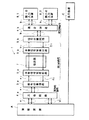
図1は、本発明の第1の実施形態に係るコンピュータ装置の構成を示すブロック図である。尚、従来構成と共通する要素には同一の符号を付している。
【0018】
図1において、第1の実施形態に係るコンピュータ装置1は、生産設備の制御装置として構成されており、演算装置Aと、第1の入力装置B1と、第2の入力装置B2と、表示装置Cと、演算装置Aと第1の入力装置B1及び第2の入力装置B2との間の信号伝送を制御する混合回路4a、4b、信号分離回路5a、5b、平衡信号変換回路6a、6bと、平衡信号伝送路7とを備えて構成されている。
【0019】
前記第1の入力装置B1はフルキーボードによるデータ入力手段、第2の入力装置B2はマウスあるいはトラックボールによるデータ入力手段である。本構成に係るコンピュータ装置1では、制御の都合上から前記演算装置Aと、第1及び第2の入力装置B1、B2、表示装置Cとの間が数メートル以上に離れた離隔地点にそれぞれを設置するため、その間の信号伝送に対して周辺機器からのノイズの影響を受けないこと、逆に周辺機器に対して不要輻射による影響を与えないようにするため、信号伝送経路に前記混合回路4a、4b、信号分離回路5a、5b、平衡信号変換回路6a、6b、平衡信号伝送路7を設けて、信号伝送を平衡信号により行う。
【0020】
以下に、コンピュータ装置1の特徴である信号伝送のための各構成要素について順を追って説明する。まず、混合回路4a、4bについて説明する。図2は混合回路の構成を示す回路図、図3は時分割信号転送のタイミング図である。
【0021】
図2において、演算装置A側の混合回路4aは、演算装置Aと第1の入力装置B1との間で相互に入出力するための双方向信号a1 と、演算装置Aと第2の入力装置B2との間で相互に入出力するための双方向信号a2 との2つの双方向信号を混合して、1つの双方向信号a3 に変換する。
【0022】
演算装置Aには、先に従来構成において示したように、第1の入力装置B1との信号伝送のための通信制御回路(LSI)25aと、第2の入力装置B2との信号伝送のための通信制御回路(LSI)26aとが設けられており、それぞれデータ信号とクロック信号とからなる2つの双方向信号a1 、a2 の入出力制御を行っている。この2つの双方向信号a1 、a2 は、前記混合回路4aに設けられた混合制御回路14aによって1つの双方向信号a3 に変換される。
【0023】
同様に、第1及び第2の入力装置B1、B2の側にも、それぞれ通信制御回路25b、26bが設けられており、第1の入力装置B1の通信制御回路25bの双方向信号b1 と、第2の入力装置B2の通信制御回路26bの双方向信号b2 とは、第1及び第2の入力装置B1、B2側の混合回路4bに設けられた混合制御回路14bによって混合され、1つの双方向信号b3 に変換される。
【0024】
演算装置Aから第1の入力装置B1または第2の入力装置B2に制御コマンドを出力するときは、演算装置A内の通信制御回路25aまたは26bから出力された2つの非同期の送信信号a1 (T)、a2 (T)は、混合回路4a内の入力ポートP1、P2、P3、P4から混合制御回路14aに入力される。この混合制御回路14aは予め設定された変換手順により、送信信号a1 (T)と送信信号a2 (T)とが1つの送信信号a3 (T)に変換され、バッファ35、36を通じて出力される。尚、前記a1 (T)、a2 (T)等の記載は、双方向信号であるa1 、a2 等の送信(Transmission)と受信(Recept)とを区別するもので、双方向信号の中の送信信号に(T)、受信信号に(R)を付している。以下の記載においても同様である。
【0025】
第1の入力装置B1または第2の入力装置B2からのデータ入力は、演算装置A側の混合回路4a内の入力ポートP5、P6から混合制御回路14aに入力される。混合制御回路14aは予め設定された変換手順により、1つの受信信号a3 (R)をデータ信号とクロック信号とで構成された2つの受信信号a1 (R)とa2 (R)とに変換し、出力バッファ31、32、33、34を通じて演算装置A内の通信制御回路25aまたは26aに出力する。
【0026】
上記演算装置A側の混合回路4aにおける動作と同様の動作が、第1及び第2の入力装置B1、B2側の混合回路4bにおいてもなされ、第1の入力装置B1の送信信号b1 (T)と第2の入力装置B2の送信信号b2 (T)とが混合されて送信信号b3 (T)として出力され、演算装置Aからの受信信号b3 (R)は受信信号b1 (R)と受信信号b2 (R)とに振り分けられて第1及び第2の入力装置B1、B2にそれぞれ入力される。
【0027】
上記混合回路4a、4bによる信号の混合動作は、図3に示すように、時分割で転送することによって行われる。
【0028】
図3は、時分割のタイミング図で、演算装置Aと第1及び第2の入力装置B1、B2との間における信号伝送の時分割内容を示している。同図において、同期(1)は演算装置Aから第1の入力装置B1へ向けての送信信号a1 (T)を送信信号a3 (T)として出力するタイミングであり、第1の入力装置B1は受信信号b1 (R)として受信する。また、同期(2)は第1の入力装置B1から演算装置Aへ向けての送信信号b1 (T)を送信信号b3 (T)として出力するタイミングであり、演算装置Aは受信信号a1 (R)として受信する。更に、同期(3)は演算装置Aから第2の入力装置B2へ向けての送信信号a2 (T)を送信信号a3 (T)として出力するタイミングであり、第2の入力装置B2は受信信号b2 (R)として受信する。更に、同期(4)は第2の入力装置B2から演算装置Aへ向けての送信信号b2 (T)を送信信号b3 (T)として出力するタイミングであり、演算装置Aは受信信号a2 (R)として受信する。以降は同期(1)から(4)までを繰り返す。
【0029】
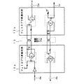
次に、信号分離回路5a、5bについて説明する。図4は信号分離回路の構成を示す回路図である。
【0030】
図4において、信号分離回路5aは、双方向信号と単方向信号とのいずれか一方を他方に変換する変換制御回路15aを備えて構成されている。演算装置Aから第1の入力装置B1または第2の入力装置B2への信号伝送するときは、先に説明した混合回路4aにより1つに混合された双方向信号a3 として出力されたデータ信号とクロック信号とが、この信号分離回路5aの入力バッファ37、38を通じて前記変換制御回路15aに入力される。変換制御回路15aは予め設定された通信手順と通信速度に準じて入力されたデータ信号に通信制御用のコマンドを付加して送信信号とし、送信信号出力バッファ39を通じて送信信号a4 を出力する。
【0031】
第1の入力装置B1または第2の入力装置B2からの入力信号は、受信信号a5 として入力バッファ40を通じて変換制御回路15aに入力される。前記変換制御回路15aは予め設定された通信手順と通信速度に準じて受信信号a5 から通信制御用コマンドを削除して演算装置Aへの入力データとし、出力バッファ41、42を通じてデータ信号とクロック信号とを混合回路4aに出力する。
【0032】
第1及び第2の入力装置B1、B2側の信号分離回路5bも同様に変換制御回路15bを備えて構成されており、前記演算装置A側の信号分離回路5aと、第1及び第2の入力装置B1、B2側の信号分離回路5bとは、予め設定された通信手順と通信速度とに従って動作する。
【0033】
次いで、平衡信号変換回路6a、6b及び伝送路7について、平衡信号回路の好ましい実施態様として、RS422規格になるRS422回路を採用した構成を図5を参照して説明する。
【0034】
図5において、演算装置A側の平衡信号変換回路6a及び第1及び第2の入力装置B1、B2側の平衡信号変換回路6bは、それぞれRS422信号変換回路として構成され、この間の平衡信号伝送路7はRS422信号伝送路として構成されている。演算装置A側の平衡信号変換回路6aは、ラインドライバ17aとラインレシーバ18aとを備えて構成され、演算装置A側の信号分離回路5aによって単方向信号に分離された送信信号a4 は、ラインドライバ17aによりRS422信号(平衡信号)に変換され、平衡信号伝送路7により伝送されて第1及び第2の入力装置B1、B2側の平衡信号変換回路6bが備えたラインレシーバ18bに入力される。このラインレシーバ18bにより単方向信号b4 に変換された受信信号は、第1及び第2の入力装置B1、B2側の信号分離回路5bに入力される。
【0035】
第1及び第2の入力装置B1、B2側の信号分離回路5bからの送信信号b5 は、平衡信号変換回路6bのラインドライバ17bでRS422信号に変換され、平衡信号伝送路7により伝送されて演算装置A側の平衡信号変換回路6aのラインレシーバ18aに入力される。このラインレシーバ18aにより単方向信号a5 に変換された受信信号は、演算装置A側の信号分離回路5bに入力される。
【0036】
この平衡信号伝送における前記ラインレシーバ18a、18bは、差動アンプとして構成されているのでコモンモードノイズは除去され、前記平衡信号伝送路7は、図示するように、より平衡度の高い2対のツイストペア線が用いられているのでノーマルモードノイズが乗りにくく、耐ノイズ性に優れた信号伝送を行うことができ、信号伝送の距離が長くなった場合にも外来ノイズによる誤動作や不要輻射による周辺機器への影響を排除することができる。
【0037】
従って、上記第1の実施形態による構成により、演算装置Aと第1及び第2の入力装置B1、B2とは、それぞれ混合回路4a、4bと、信号分離回路5a、5bと、平衡信号変換回路6a、6bとにより、平衡信号伝送路7で接続できるので、周辺機器からのノイズによる影響を受け難く、また、逆に周辺機器に電磁障害を与えないので、生産設備内で演算装置Aと第1及び第2の入力装置B1、B2とを離隔地点に設置したような場合でも正常な動作を確保できる。
【0038】
次に、本発明の第2の実施形態に係るコンピュータ装置について説明する。図6は第2の実施形態に係るコンピュータ装置の構成を示すブロック図、図7は光信号変換回路の構成を示すブロック図である。尚、先の構成と共通する要素には同一の符号を付し、その説明は省略する。
【0039】
図6において、第2の実施形態に係るコンピュータ装置2は、演算装置Aと第1及び第2の入力装置B1、B2とにそれぞれ設けられた信号分離回路5aと信号分離回路5bとの間の単方向信号a4 、a5 、b4 、b5 を、それぞれ光信号変換回路10a、10bによって光信号に変換し、光ケーブル11により相互に伝送できるように構成されている。
【0040】
前記光信号変換回路10a、10bは、図7に示すように構成されている。光信号変換回路10a、10bにはそれぞれ電気−光変換回路19a、19bと、光−電気変換回路20a、20bとが設けられており、TTLレベル信号の送信信号a4 、b5 は、それぞれ電気−光変換回路19a、19bにより光信号に変換されて光ケーブル11で伝送される。光ケーブル11で伝送されてきた光信号は、光−電気変換回路20a、20bでそれぞれTTLレベル信号の受信信号a5 、b4 に変換される。
【0041】
光信号による信号伝送は、信号伝送路を電気的に絶縁することになるので、原理的にコモンモードノイズを除去することができ、第1の実施形態において説明した平衡信号伝送において除去できないような大きなコモンモードノイズに対しても有効に作用する。従って、本構成になるコンピュータ装置2は、ノイズ発生源の多い生産設備等に演算装置Aと入力装置Bとを離隔地点に設置したような状態でも、周辺機器からのノイズの影響を受け難く、特に大きな誘導ノイズの発生源があるような環境では有効である。また、光信号伝送は原理的にも電磁輻射を発生させないので、周辺機器に電磁障害を与えることがない。
【0042】
上記したごとく、周辺ノイズの影響を受け難い光信号変換による信号伝送路の絶縁の構成は、図8に示すように、フォトカプラを用いて構成することもできる。
【0043】
図8は、演算装置A側に設けられた信号分離回路5aと、第1及び第2の入力装置B1、B2側に設けられた信号分離回路5bとの間に、それぞれフォトカプラ絶縁回路12a、12bを設け、その間を2対のツイストペア線による絶縁信号ケーブル13で接続したものである。この構成での信号伝送はカレントループ伝送となるため、線路抵抗やノイズの影響を受け難く、また信号伝送路は絶縁されるので、伝送経路上に混入したノイズが遮断され、よりノイズに強い信号伝送を実現することができる。
【0044】
次いで、第1及び第2の実施形態において説明した混合回路4a、4bの時分割転送方式のより好ましい態様を本発明の第3の実施形態として説明する。図9は第3の実施形態に係る混合回路の構成を示すブロック図、図10は信号伝送の状態を説明する模式図である。
【0045】
本実施形態では、演算装置A側の混合回路21aをマスターとし、第1及び第2の入力装置B1、B2側の混合回路21bをスレーブとして、マスターである混合回路21aの同期タイミングに従って、スレーブである混合回路21bが動作するように構成されている。更に、図10に示すように、混合回路21a(または混合回路21b)から出力される双方向信号a3 (b3 )は、バケット1とバケット2とにより構成され、前記バケット1には第1の入力装置B1と第2の入力装置B2との区分、前記バケット2には転送するコマンドデータやステータス情報が載せられ、バケット2に転送するコマンドデータやステータス情報がない場合には、マスターとスレーブとの間で予め設定されたダミーデータを転送する時分割転送方式として構成されている。この構成により、2つの非同期の双方向信号a1 、a2 (b1 、b2 )を同期化して時分割に転送し、1つの双方向信号a3 (b3 )とする。
【0046】
図9において、演算装置A側の混合回路21aがマスターとして、第1及び第2の入力装置B1、B2側の混合回路21bがスレーブとして動作する。まず、混合回路21aが混合回路21bに向けて混合信号a3 (T)を出力する場合と、混合回路21bから混合回路21aに混合信号a3 (R)を入力する場合との混合回路21aの動作について説明する。
【0047】
演算装置Aから第1の入力装置B1への送信信号a1 (T)、演算装置Aから第2の入力装置B2への送信信号a2 (T)がそれぞれ送信信号入力部43、44に入力されると、送信信号a1 (T)、a2 (T)は同期タイミングで出力するまで待機のため、それぞれ出力データ記憶部45、46に記憶される。この出力データ記憶部45、46には、前記送信信号入力部43、44に信号入力がないときに出力する予め設定されたダミーデータも記憶されている。前記出力データ記憶部45、46に一時記憶された出力データは、転送部47により同期タイミング発生部22からの同期タイミングに従ってバケット1に第1の入力装置B1、第2の入力装置B2の区別、バケット2に出力データ記憶部45と出力データ記憶部46とから該当する出力データが転送され、この出力データは出力部48により同期タイミング発生部22からの同期タイミングに従ってスレーブである第1及び第2の入力装置B1、B2に向けて混合信号a3 (T)として出力される。
【0048】
混合回路21bからの混合信号a3 (R)を入力するときには、混合信号a3 (R)が入力部49に入力されると、入力装置検出部50において入力データのバケット1から第1の入力装置B1、第2の入力装置B2の区別が検出され、検出された入力装置の区分に該当するバケット2のデータはそれぞれ入力データ記憶部51、52に配分されて演算装置Aに出力するまで記憶され、この入力データ記憶部51、52に記憶された内容が予め設定されたダミーデータでないとき受信信号出力部53、54からそれぞれ受信信号a1 (R)、a2 (R)として演算装置Aに出力される。
【0049】
次に、スレーブ側の混合回路21bに混合回路21aからの混合信号b3 (R)を入力する場合と、混合回路21bが混合回路21aに向けて混合信号b3 (T)を出力する場合との混合回路21bの動作について説明する。
【0050】
混合回路21aからの混合信号b3 (R)を入力するときには、混合信号b3 (R)が入力部55に入力されると、同期タイミング検出部23により混合信号b3 (R)のデータから同期タイミングが検出され、出力データ転送部56は混合信号b3 (R)のバケット1から入力装置B1、B2の区別を判別し、該当するデータはそれぞれ出力データ記憶部57、58に第1の入力装置及び第2の入力装置B2に出力するまで記憶され、この出力データ記憶部57、58に記憶された内容が予め設定されたダミーデータでないとき受信信号出力部59、60からそれぞれ第1の入力装置B1または第2の入力装置B2にそれぞれ受信号b1 (R)、b2 (R)として出力される。
【0051】
第1及び第2の入力装置B1、B2からの送信信号b1 (T)、b2 (T)を出力するときには、送信信号b1 (T)、b2 (T)がそれぞれ送信信号入力部61、62に入力されると、送信信号b1 (T)、b2 (T)の内容を混合信号b3 として出力するまで待機のため、それぞれ入力データ記憶部63、64に記憶される。この入力データ記憶部63、64には、前記送信信号入力部61、62に信号入力がないときに出力する予め設定されたダミーデータも記憶されている。前記入力データ記憶部63、64に一時記憶された入力データは、入力データ転送部65により同期タイミング検出部23からの同期タイミングに従ってバケット1に第1の入力装置B1、第2の入力装置B2の区別、バケット2に入力データ記憶部63と入力データ記憶部64とから該当する入力データが転送され、この入力データは出力部66により同期タイミング検出部23からの同期タイミングに従ってマスターである演算装置Aに向けて混合信号b3 (T)として出力される。
【0052】
上記動作により、演算部Aから第1の入力装置B1または第2の入力装置B2への2つの送信信号a1 (T)、a2 (T)は、1つの混合信号a3 (T)として混合回路21aから出力され、信号分離回路5a、平衡信号変換回路6a、平衡信号伝送路7、平衡信号変換回路6b、信号分離回路5bを通じて混合信号b3 (R)として第1及び第2の入力装置B1、B2側の混合回路21bに伝送され、受信信号b1 (R)は第1の入力装置B1に、受信信号b2 (R)は第2の入力装置B2に入力される。また、第1の入力装置B1からの送信信号b1 (T)及び第2の入力装置B2からの送信信号b2 (T)は混合回路21bにより混合され混合信号b3 (T)として出力され、信号分離回路5b、平衡信号変換回路6b、平衡信号伝送路7、平衡信号変換回路6a、信号分離回路5aを通じて混合信号a3 (R)として演算装置A側の混合回路21aに伝送され、第1の入力装置B1からの受信信号a1 (R)と第2の入力装置B2からの受信信号a2 (R)として演算装置Aに入力される。
【0053】
以上説明した各実施形態において、第1の入力装置B1内の通信制御回路25bに第2の入力装置B2の通信制御回路26b、混合回路4b、信号分離回路5bを一体的にLSIとして構成することもできる。第2の入力装置B2はマウスまたはトラックボールであり、回路構成の収容に制限があるため、この構成により具体化することができる。
【0054】
【発明の効果】
以上の説明の通り本願の第1発明によれば、演算装置と第1及び第2の入力装置との間の2つの双方向信号は、送信側において1つの双方向信号に混合多重化して伝送し、受信側においては、多重化している1つの双方向信号を第1及び第2の入力装置に対応する2つの双方向信号に戻して演算装置と第1及び第2の入力装置との間で互いの信号を入出力させられる。
【図面の簡単な説明】
【図1】本発明の第1の実施形態に係るコンピュータ装置の構成を示すブロック図。
【図2】上記構成における信号分離回路の構成を示す回路図。
【図3】上記構成における時分割の同期タイミング図。
【図4】上記構成における信号分離回路の構成を示す回路図。
【図5】上記構成における平衡信号変換回路の構成を示す回路図。
【図6】本発明の第2の実施形態に係るコンピュータ装置の構成を示すブロック図。
【図7】上記構成における光信号変換回路の構成を示す回路図。
【図8】光信号変換と平衡信号変換とを併用した信号伝送の構成を示す回路図。
【図9】本発明の第3の実施形態に係る混合回路の構成を示すブロック図。
【図10】上記構成における同期タイミング図。
【図11】従来例に係るコンピュータ装置の構成を示すブロック図。
【図12】従来構成に係る信号伝送の構成を示す回路図。
【符号の説明】
1、2 コンピュータ装置
4a、4b 混合回路
5a、5b 信号分離回路
6a、6b 平衡信号変換回路
7 平衡信号伝送路
10a、10b 光信号変換回路
11 光ケーブル
21a、21b 混合回路
A 演算装置
B1 第1の入力装置
B2 第2の入力装置
C 表示装置[0001]
BACKGROUND OF THE INVENTION
The present invention relates to a computer device including an arithmetic device, an input device, and a display device, and in particular, the input device is two input devices of a full keyboard and a pointing device, and the two input devices are separated from the arithmetic device. The present invention relates to a computer device that can be placed at a place.
[0002]
[Prior art]
In a personal computer, an input device including a full keyboard and a mouse or a trackball has a general configuration. The configuration of such a computer apparatus is shown in FIGS.
[0003]
FIG. 11 is a block diagram showing a configuration of a computer device 30 according to the prior art, a computing device A, a first input device B1 using a full keyboard, a second input device B2 using a mouse or a trackball, and a display device. C. The arithmetic device A and the first input device B1 and the second input device B2 are connected by bidirectional
[0004]
FIG. 12 is a circuit diagram showing a configuration of signal transmission between the arithmetic device A and the first input device B1 of the computer device 30, and between the arithmetic device A and the second input device B2. The arithmetic device A has a
[0005]
[Problems to be solved by the invention]
When the computer device configured as described above is used as a control device for production equipment, the installation location of the arithmetic device and the installation locations of the first and second input devices and the display device are separated by several meters or more. You may have to do that. When the arithmetic device and the input device are installed apart from each other in this manner, malfunctions may occur due to noise from peripheral devices mixed in the control signal between them, or conversely, the control signal may be transmitted to the peripheral devices. May cause electromagnetic interference.
[0006]
It is an object of the present invention to provide a computer apparatus that employs a signal transmission method that does not cause a failure as described above even when an arithmetic device and an input device are installed at remote locations.
[0007]
[Means for Solving the Problems]
1st invention of this application is provided with the arithmetic device, the 1st input device, and the 2nd input device, and is bidirectional between the said arithmetic device, the said 1st input device, and the 2nd input device. In the computer device for signal transmission, the first input deviceBidirectional signal corresponding toAnd second input deviceIn placeCorrespondingTwoDirection signalAndIn addition, the transmission signal and the reception signal are time-divided and mixed into one bidirectional signal, and the bidirectional signal mixed into this one is input to the first input device.Bidirectional signal corresponding toAnd a second input deviceTwoDirection signalAndA mixing circuit to be returned is provided on both the arithmetic device side and the first and second input device sides, and the mixing circuit is provided between the arithmetic device and the first and second input devices. A mixed signal is transmitted.
[0008]
According to the above configuration, between the arithmetic device and the first and second input devices.Corresponding to themOn the transmitting side, the two bidirectional signals are time-divided including a transmission signal and a reception signal by a mixing circuit and mixed into one bidirectional signal and transmitted on the transmission line. On the reception side, the transmission signal and One bidirectional signal mixed in a time-division manner including the received signal is returned to two bidirectional signals corresponding to the first and second input devices, and the arithmetic device and the first and second input devices Mutual signals are input and output between
[0009]
The computer device is,flatThe balance signal conversion circuit can be configured by using an RS422 signal conversion circuit. The RS422 is a balanced digital voltage interface, and the electrical characteristics of balanced signal transmission are defined, and the balanced signal transmission is less susceptible to noise. Can be adopted.
[0010]
In addition, the computer apparatus of the present application separates the bidirectional signal in the mixed transmission path into a transmission signal and a reception signal on a single transmission path, and returns the unidirectional signal to the bidirectional signal. A signal separation circuit and an optical signal conversion circuit that converts the unidirectional signal into an optical signal and returns the optical signal to the unidirectional signal are provided in both the arithmetic device and the input device, and the arithmetic device The optical signal conversion circuit on the side and the optical signal conversion circuit on the input device side are connected by an optical cable.
[0016]
DETAILED DESCRIPTION OF THE INVENTION
Hereinafter, an embodiment of the present invention will be described with reference to the accompanying drawings for understanding of the present invention. The following embodiment is an example embodying the present invention, and does not limit the technical scope of the present invention.
[0017]
FIG. 1 is a block diagram showing a configuration of a computer apparatus according to the first embodiment of the present invention. In addition, the same code | symbol is attached | subjected to the element which is common in a conventional structure.
[0018]
In FIG. 1, a
[0019]
The first input device B1 is data input means using a full keyboard, and the second input device B2 is data input means using a mouse or a trackball. In the
[0020]
Hereinafter, each component for signal transmission that is a feature of the
[0021]
In FIG. 2, the mixing
[0022]
The arithmetic unit A includes a communication control circuit (LSI) 25a for signal transmission with the first input device B1 and a signal transmission with the second input device B2 as previously shown in the conventional configuration. Communication control circuit (LSI) 26a, and two bidirectional signals a each comprising a data signal and a clock signal.1, A2I / O control is performed. These two bidirectional signals a1, A2Is generated by the mixing
[0023]
Similarly,
[0024]
When a control command is output from the arithmetic device A to the first input device B1 or the second input device B2, two asynchronous transmission signals a output from the
[0025]
Data input from the first input device B1 or the second input device B2 is input to the mixing
[0026]
An operation similar to the operation in the
[0027]
The mixing operation of the signals by the mixing
[0028]
FIG. 3 is a timing diagram of time division, and shows time division contents of signal transmission between the arithmetic unit A and the first and second input devices B1 and B2. In the figure, synchronization (1) is a transmission signal a from the arithmetic unit A to the first input unit B1.1(T) is transmitted signal aThree(T) is the output timing, and the first input device B1 receives the received signal b.1Receive as (R). The synchronization (2) is a transmission signal b from the first input device B1 to the arithmetic device A.1(T) is transmitted signal bThree(T) is the timing of output, and the arithmetic unit A receives the received signal a1Receive as (R). Further, the synchronization (3) is a transmission signal a from the arithmetic device A to the second input device B2.2(T) is transmitted signal aThree(T) is the output timing, and the second input device B2 receives the received signal b.2Receive as (R). Further, synchronization (4) is a transmission signal b from the second input device B2 to the arithmetic device A.2(T) is transmitted signal bThree(T) is the timing of output, and the arithmetic unit A receives the received signal a2Receive as (R). Thereafter, synchronization (1) to (4) is repeated.
[0029]
Next, the
[0030]
In FIG. 4, the signal separation circuit 5a includes a
[0031]
The input signal from the first input device B1 or the second input device B2 is the received signal a.FiveIs input to the
[0032]
Similarly, the
[0033]
Next, with respect to the balanced
[0034]
In FIG. 5, the balanced
[0035]
Transmission signal b from the
[0036]
Since the line receivers 18a and 18b in this balanced signal transmission are configured as differential amplifiers, common mode noise is removed, and the balanced
[0037]
Therefore, with the configuration according to the first embodiment, the arithmetic unit A and the first and second input devices B1 and B2 include the mixing
[0038]
Next, a computer apparatus according to the second embodiment of the present invention will be described. FIG. 6 is a block diagram showing a configuration of a computer apparatus according to the second embodiment, and FIG. 7 is a block diagram showing a configuration of an optical signal conversion circuit. In addition, the same code | symbol is attached | subjected to the element which is common in a previous structure, and the description is abbreviate | omitted.
[0039]
In FIG. 6, the
[0040]
The optical signal conversion circuits 10a and 10b are configured as shown in FIG. The optical signal conversion circuits 10a and 10b are provided with electrical-
[0041]
Since the signal transmission by the optical signal electrically insulates the signal transmission path, the common mode noise can be removed in principle and cannot be removed in the balanced signal transmission described in the first embodiment. It works effectively against large common mode noise. Therefore, the
[0042]
As described above, the signal transmission path insulation configuration by optical signal conversion which is not easily affected by ambient noise can be configured using a photocoupler as shown in FIG.
[0043]
FIG. 8 shows a photocoupler insulation circuit 12a between a signal separation circuit 5a provided on the arithmetic device A side and a
[0044]
Next, a more preferable aspect of the time division transfer method of the mixing
[0045]
In this embodiment, the mixing circuit 21a on the arithmetic unit A side is a master, the mixing circuit 21b on the first and second input devices B1 and B2 side is a slave, and the slave is in accordance with the synchronization timing of the mixing circuit 21a that is the master. A certain mixing circuit 21b is configured to operate. Furthermore, as shown in FIG. 10, the bidirectional signal a output from the mixing circuit 21a (or the mixing circuit 21b).Three(BThree) Is composed of a
[0046]
In FIG. 9, the mixing circuit 21a on the arithmetic device A side operates as a master, and the mixing circuit 21b on the first and second input devices B1 and B2 operates as a slave. First, the mixing circuit 21a is directed to the mixing circuit 21b.ThreeWhen (T) is output, the mixed signal a is sent from the mixing circuit 21b to the mixing circuit 21a.ThreeThe operation of the mixing circuit 21a when inputting (R) will be described.
[0047]
Transmission signal a from arithmetic device A to first input device B11(T), a transmission signal a from the arithmetic device A to the second input device B2.2When (T) is input to the transmission signal input units 43 and 44, respectively, the transmission signal a1(T), a2(T) is stored in the output data storage units 45 and 46 for waiting until output at the synchronization timing. The output data storage units 45 and 46 also store preset dummy data that is output when there is no signal input to the transmission signal input units 43 and 44. The output data temporarily stored in the output data storage units 45 and 46 is transferred to the
[0048]
Mixed signal a from mixing circuit 21bThreeWhen inputting (R), the mixed signal aThreeWhen (R) is input to the input unit 49, the input device detection unit 50 detects the distinction between the first input device B1 and the second input device B2 from the
[0049]
Next, the mixing signal b from the mixing circuit 21a is sent to the mixing circuit 21b on the slave side.ThreeWhen (R) is input, the mixing circuit 21b is directed to the mixing circuit 21a.ThreeThe operation of the mixing circuit 21b when outputting (T) will be described.
[0050]
Mixed signal b from mixing circuit 21aThreeWhen inputting (R), the mixed signal bThreeWhen (R) is input to the input unit 55, the mixed timing b is detected by the synchronization timing detection unit 23.ThreeThe synchronization timing is detected from the data (R), and the output data transfer unit 56 receives the mixed signal b.ThreeThe distinction between the input devices B1 and B2 is determined from the
[0051]
Transmission signal b from the first and second input devices B1 and B21(T), b2When outputting (T), the transmission signal b1(T), b2When (T) is input to the transmission signal input units 61 and 62, respectively, the transmission signal b1(T), b2The content of (T) is mixed signal bThreeAre stored in the input data storage units 63 and 64, respectively, for waiting until output as. The input data storage units 63 and 64 also store preset dummy data that is output when no signal is input to the transmission signal input units 61 and 62. The input data temporarily stored in the input data storage units 63 and 64 is stored in the
[0052]
With the above operation, two transmission signals a from the arithmetic unit A to the first input device B1 or the second input device B2 are transmitted.1(T), a2(T) is one mixed signal aThree(T) is output from the mixing circuit 21a, and the mixed signal b is transmitted through the signal separation circuit 5a, the balanced
[0053]
In each of the embodiments described above, the
[0054]
【The invention's effect】
As described above, according to the first invention of the present application, two bidirectional signals between the arithmetic device and the first and second input devices are transmitted on the transmission side.On the receiving side, one multiplexed bi-directional signal is returned to two bi-directional signals corresponding to the first and second input devices. Mutual signals can be input / output between the first and second input devices.
[Brief description of the drawings]
FIG. 1 is a block diagram showing a configuration of a computer device according to a first embodiment of the present invention.
FIG. 2 is a circuit diagram showing a configuration of a signal separation circuit in the above configuration.
FIG. 3 is a timing diagram of time division synchronization in the above configuration.
FIG. 4 is a circuit diagram showing a configuration of a signal separation circuit in the above configuration.
FIG. 5 is a circuit diagram showing a configuration of a balanced signal conversion circuit in the above configuration.
FIG. 6 is a block diagram showing a configuration of a computer device according to a second embodiment of the present invention.
FIG. 7 is a circuit diagram showing a configuration of an optical signal conversion circuit in the above configuration.
FIG. 8 is a circuit diagram showing a configuration of signal transmission using both optical signal conversion and balanced signal conversion.
FIG. 9 is a block diagram showing a configuration of a mixing circuit according to a third embodiment of the present invention.
FIG. 10 is a synchronization timing chart in the above configuration.
FIG. 11 is a block diagram showing a configuration of a computer device according to a conventional example.
FIG. 12 is a circuit diagram showing a configuration of signal transmission according to a conventional configuration.
[Explanation of symbols]
1, 2 Computer equipment
4a, 4b mixing circuit
5a, 5b Signal separation circuit
6a, 6b Balanced signal conversion circuit
7 Balanced signal transmission line
10a, 10b Optical signal conversion circuit
11 Optical cable
21a, 21b mixing circuit
A arithmetic unit
B1 first input device
B2 Second input device
C display device
Claims (4)
前記第1の入力装置に対応する双方向信号と第2の入力装置に対応する双方向信号とを、送信信号および受信信号も含めて時分割して1つの双方向信号に混合すると共に、この1つに混合された双方向信号を第1の入力装置に対応する双方向信号と第2の入力装置に対応する双方向信号とに戻す混合回路を、前記演算装置の側と前記第1及び第2の入力装置の側との双方に備え、前記演算装置と前記第1及び第2の入力装置との間で、前記混合回路により混合した信号の伝送がなされることを特徴とするコンピュータ装置。A computer apparatus comprising an arithmetic device, a first input device, and a second input device, wherein bidirectional signal transmission is performed between the arithmetic device, the first input device, and the second input device In
A bidirectional signal that corresponds to the bidirectional signal and a second input equipment corresponding to said first input device, as well as mixed into one bidirectional signal by time division, including transmit and receive signals the mixing circuit back to the bidirectional signal that corresponds to the bidirectional signal and a second input equipment the corresponding mixed bidirectional signal to this one to the first input device, the side of the arithmetic unit In both the first and second input devices, the mixed signal is transmitted by the mixing circuit between the arithmetic device and the first and second input devices. A computer device.
前記単方向信号を平衡信号に変換すると共に、前記平衡信号を前記単方向信号に戻す平衡信号変換回路と、
を前記演算装置と前記入力装置との双方に備え、
前記演算装置側の平衡信号変換回路と前記入力装置側の平衡信号変換回路との間を平衡信号伝送路で接続したことを特徴とする請求項1に記載のコンピュータ装置。A signal separation circuit for separating a bidirectional signal in a transmission line mixed into one into a transmission signal and a reception signal on a single transmission line, and returning the unidirectional signal to the bidirectional signal;
A balanced signal conversion circuit that converts the unidirectional signal to a balanced signal and returns the balanced signal to the unidirectional signal;
For both the arithmetic unit and the input device,
2. The computer apparatus according to claim 1, wherein a balanced signal transmission path is connected between the balanced signal conversion circuit on the arithmetic device side and the balanced signal conversion circuit on the input device side.
前記単方向信号を光信号に変換すると共に、前記光信号を前記単方向信号に戻す光信号変換回路と、
を前記演算装置と前記入力装置との双方に備え、
前記演算装置側の光信号変換回路と前記入力装置側の光信号変換回路との間を光ケーブルで接続したことを特徴とする請求項1に記載のコンピュータ装置。 A signal separation circuit for separating a bidirectional signal in a transmission line mixed into one into a transmission signal and a reception signal on a single transmission line, and returning the unidirectional signal to the bidirectional signal;
An optical signal conversion circuit for converting the unidirectional signal into an optical signal and returning the optical signal to the unidirectional signal;
For both the arithmetic unit and the input device,
Computer equipment according to claim 1, characterized in that between the optical signal conversion circuit of the input device side and the optical signal conversion circuit of the operational device side connected by optical cable.
Priority Applications (1)
| Application Number | Priority Date | Filing Date | Title |
|---|---|---|---|
| JP03739997A JP3992775B2 (en) | 1997-02-21 | 1997-02-21 | Computer equipment |
Applications Claiming Priority (1)
| Application Number | Priority Date | Filing Date | Title |
|---|---|---|---|
| JP03739997A JP3992775B2 (en) | 1997-02-21 | 1997-02-21 | Computer equipment |
Publications (2)
| Publication Number | Publication Date |
|---|---|
| JPH10240406A JPH10240406A (en) | 1998-09-11 |
| JP3992775B2 true JP3992775B2 (en) | 2007-10-17 |
Family
ID=12496461
Family Applications (1)
| Application Number | Title | Priority Date | Filing Date |
|---|---|---|---|
| JP03739997A Expired - Fee Related JP3992775B2 (en) | 1997-02-21 | 1997-02-21 | Computer equipment |
Country Status (1)
| Country | Link |
|---|---|
| JP (1) | JP3992775B2 (en) |
Families Citing this family (3)
| Publication number | Priority date | Publication date | Assignee | Title |
|---|---|---|---|---|
| JP5604649B2 (en) * | 2011-12-20 | 2014-10-08 | 株式会社ソフイア | Game machine |
| JP5706305B2 (en) * | 2011-12-20 | 2015-04-22 | 株式会社ソフイア | Game machine |
| JP5604650B2 (en) * | 2011-12-20 | 2014-10-08 | 株式会社ソフイア | Game machine |
-
1997
- 1997-02-21 JP JP03739997A patent/JP3992775B2/en not_active Expired - Fee Related
Also Published As
| Publication number | Publication date |
|---|---|
| JPH10240406A (en) | 1998-09-11 |
Similar Documents
| Publication | Publication Date | Title |
|---|---|---|
| EP0533167A2 (en) | Optical communication system having transmission line switching system | |
| JPS60169253A (en) | Communication network having master-slave type series structure | |
| US6078974A (en) | Method and apparatus for extension of bi-directional open collector signals in a multiplexed data transmission system | |
| JPH10240406A (en) | Computer equipment | |
| US4532627A (en) | Time multiplex controlled data system | |
| JP3983331B2 (en) | Computer equipment | |
| JP3881088B2 (en) | Computer equipment | |
| JPH10207591A (en) | Interface board | |
| JPS607577Y2 (en) | data transmission equipment | |
| JP3983330B2 (en) | Computer apparatus, electronic component mounting apparatus using the same, and control method in computer apparatus | |
| JP2677274B2 (en) | Variable length serial data communication system | |
| EP0063140A1 (en) | Data communication bus structure | |
| JPS5992653A (en) | Data transmitter | |
| JPS58172039A (en) | Optical transmission system | |
| JPH0530069A (en) | Control signal transmission system | |
| JPS61101142A (en) | Data protection circuit | |
| SU1118999A1 (en) | Interface for linking informational computer system with sequential multiplexor channel | |
| JPH0795734B2 (en) | Circuit for polling communication | |
| JPH05199273A (en) | Signal isolated transmission device | |
| JPH0237148B2 (en) | DEETADENSOSHISUTEMU | |
| JPH0230256A (en) | Two-way serial communication system | |
| JPS61131935A (en) | Data transmission control system | |
| JPS63203027A (en) | Optical relay transmission system | |
| JP2000165365A (en) | Information transfer system | |
| JPS59183554A (en) | System for detecting collision of optical network of bus structure |
Legal Events
| Date | Code | Title | Description |
|---|---|---|---|
| A621 | Written request for application examination |
Free format text: JAPANESE INTERMEDIATE CODE: A621 Effective date: 20040116 |
|
| A977 | Report on retrieval |
Free format text: JAPANESE INTERMEDIATE CODE: A971007 Effective date: 20051121 |
|
| A131 | Notification of reasons for refusal |
Free format text: JAPANESE INTERMEDIATE CODE: A131 Effective date: 20051227 |
|
| A521 | Written amendment |
Free format text: JAPANESE INTERMEDIATE CODE: A523 Effective date: 20060227 |
|
| A02 | Decision of refusal |
Free format text: JAPANESE INTERMEDIATE CODE: A02 Effective date: 20060919 |
|
| A521 | Written amendment |
Free format text: JAPANESE INTERMEDIATE CODE: A523 Effective date: 20061120 |
|
| A911 | Transfer of reconsideration by examiner before appeal (zenchi) |
Free format text: JAPANESE INTERMEDIATE CODE: A911 Effective date: 20070117 |
|
| TRDD | Decision of grant or rejection written | ||
| A01 | Written decision to grant a patent or to grant a registration (utility model) |
Free format text: JAPANESE INTERMEDIATE CODE: A01 Effective date: 20070626 |
|
| A61 | First payment of annual fees (during grant procedure) |
Free format text: JAPANESE INTERMEDIATE CODE: A61 Effective date: 20070725 |
|
| R150 | Certificate of patent or registration of utility model |
Free format text: JAPANESE INTERMEDIATE CODE: R150 |
|
| FPAY | Renewal fee payment (event date is renewal date of database) |
Free format text: PAYMENT UNTIL: 20100803 Year of fee payment: 3 |
|
| FPAY | Renewal fee payment (event date is renewal date of database) |
Free format text: PAYMENT UNTIL: 20110803 Year of fee payment: 4 |
|
| FPAY | Renewal fee payment (event date is renewal date of database) |
Free format text: PAYMENT UNTIL: 20110803 Year of fee payment: 4 |
|
| FPAY | Renewal fee payment (event date is renewal date of database) |
Free format text: PAYMENT UNTIL: 20120803 Year of fee payment: 5 |
|
| FPAY | Renewal fee payment (event date is renewal date of database) |
Free format text: PAYMENT UNTIL: 20130803 Year of fee payment: 6 |
|
| S533 | Written request for registration of change of name |
Free format text: JAPANESE INTERMEDIATE CODE: R313533 |
|
| R350 | Written notification of registration of transfer |
Free format text: JAPANESE INTERMEDIATE CODE: R350 |
|
| S111 | Request for change of ownership or part of ownership |
Free format text: JAPANESE INTERMEDIATE CODE: R313113 |
|
| R350 | Written notification of registration of transfer |
Free format text: JAPANESE INTERMEDIATE CODE: R350 |
|
| LAPS | Cancellation because of no payment of annual fees |