JP4002143B2 - Manufacturing method of semiconductor device - Google Patents
Manufacturing method of semiconductor device Download PDFInfo
- Publication number
- JP4002143B2 JP4002143B2 JP2002200930A JP2002200930A JP4002143B2 JP 4002143 B2 JP4002143 B2 JP 4002143B2 JP 2002200930 A JP2002200930 A JP 2002200930A JP 2002200930 A JP2002200930 A JP 2002200930A JP 4002143 B2 JP4002143 B2 JP 4002143B2
- Authority
- JP
- Japan
- Prior art keywords
- lands
- semiconductor device
- substrate
- semiconductor chip
- resin sealing
- Prior art date
- Legal status (The legal status is an assumption and is not a legal conclusion. Google has not performed a legal analysis and makes no representation as to the accuracy of the status listed.)
- Expired - Fee Related
Links
Images








Classifications
-
- H—ELECTRICITY
- H10—SEMICONDUCTOR DEVICES; ELECTRIC SOLID-STATE DEVICES NOT OTHERWISE PROVIDED FOR
- H10W—GENERIC PACKAGES, INTERCONNECTIONS, CONNECTORS OR OTHER CONSTRUCTIONAL DETAILS OF DEVICES COVERED BY CLASS H10
- H10W72/00—Interconnections or connectors in packages
-
- H—ELECTRICITY
- H10—SEMICONDUCTOR DEVICES; ELECTRIC SOLID-STATE DEVICES NOT OTHERWISE PROVIDED FOR
- H10W—GENERIC PACKAGES, INTERCONNECTIONS, CONNECTORS OR OTHER CONSTRUCTIONAL DETAILS OF DEVICES COVERED BY CLASS H10
- H10W74/00—Encapsulations, e.g. protective coatings
- H10W74/01—Manufacture or treatment
- H10W74/014—Manufacture or treatment using batch processing
-
- H—ELECTRICITY
- H10—SEMICONDUCTOR DEVICES; ELECTRIC SOLID-STATE DEVICES NOT OTHERWISE PROVIDED FOR
- H10W—GENERIC PACKAGES, INTERCONNECTIONS, CONNECTORS OR OTHER CONSTRUCTIONAL DETAILS OF DEVICES COVERED BY CLASS H10
- H10W70/00—Package substrates; Interposers; Redistribution layers [RDL]
- H10W70/60—Insulating or insulated package substrates; Interposers; Redistribution layers
- H10W70/62—Insulating or insulated package substrates; Interposers; Redistribution layers characterised by their interconnections
- H10W70/65—Shapes or dispositions of interconnections
-
- H—ELECTRICITY
- H10—SEMICONDUCTOR DEVICES; ELECTRIC SOLID-STATE DEVICES NOT OTHERWISE PROVIDED FOR
- H10W—GENERIC PACKAGES, INTERCONNECTIONS, CONNECTORS OR OTHER CONSTRUCTIONAL DETAILS OF DEVICES COVERED BY CLASS H10
- H10W74/00—Encapsulations, e.g. protective coatings
- H10W74/01—Manufacture or treatment
-
- H—ELECTRICITY
- H10—SEMICONDUCTOR DEVICES; ELECTRIC SOLID-STATE DEVICES NOT OTHERWISE PROVIDED FOR
- H10W—GENERIC PACKAGES, INTERCONNECTIONS, CONNECTORS OR OTHER CONSTRUCTIONAL DETAILS OF DEVICES COVERED BY CLASS H10
- H10W90/00—Package configurations
- H10W90/701—Package configurations characterised by the relative positions of pads or connectors relative to package parts
-
- H—ELECTRICITY
- H10—SEMICONDUCTOR DEVICES; ELECTRIC SOLID-STATE DEVICES NOT OTHERWISE PROVIDED FOR
- H10W—GENERIC PACKAGES, INTERCONNECTIONS, CONNECTORS OR OTHER CONSTRUCTIONAL DETAILS OF DEVICES COVERED BY CLASS H10
- H10W72/00—Interconnections or connectors in packages
- H10W72/01—Manufacture or treatment
- H10W72/0198—Manufacture or treatment batch processes
-
- H—ELECTRICITY
- H10—SEMICONDUCTOR DEVICES; ELECTRIC SOLID-STATE DEVICES NOT OTHERWISE PROVIDED FOR
- H10W—GENERIC PACKAGES, INTERCONNECTIONS, CONNECTORS OR OTHER CONSTRUCTIONAL DETAILS OF DEVICES COVERED BY CLASS H10
- H10W72/00—Interconnections or connectors in packages
- H10W72/071—Connecting or disconnecting
- H10W72/075—Connecting or disconnecting of bond wires
-
- H—ELECTRICITY
- H10—SEMICONDUCTOR DEVICES; ELECTRIC SOLID-STATE DEVICES NOT OTHERWISE PROVIDED FOR
- H10W—GENERIC PACKAGES, INTERCONNECTIONS, CONNECTORS OR OTHER CONSTRUCTIONAL DETAILS OF DEVICES COVERED BY CLASS H10
- H10W72/00—Interconnections or connectors in packages
- H10W72/50—Bond wires
- H10W72/551—Materials of bond wires
-
- H—ELECTRICITY
- H10—SEMICONDUCTOR DEVICES; ELECTRIC SOLID-STATE DEVICES NOT OTHERWISE PROVIDED FOR
- H10W—GENERIC PACKAGES, INTERCONNECTIONS, CONNECTORS OR OTHER CONSTRUCTIONAL DETAILS OF DEVICES COVERED BY CLASS H10
- H10W72/00—Interconnections or connectors in packages
- H10W72/90—Bond pads, in general
- H10W72/951—Materials of bond pads
-
- H—ELECTRICITY
- H10—SEMICONDUCTOR DEVICES; ELECTRIC SOLID-STATE DEVICES NOT OTHERWISE PROVIDED FOR
- H10W—GENERIC PACKAGES, INTERCONNECTIONS, CONNECTORS OR OTHER CONSTRUCTIONAL DETAILS OF DEVICES COVERED BY CLASS H10
- H10W74/00—Encapsulations, e.g. protective coatings
-
- H—ELECTRICITY
- H10—SEMICONDUCTOR DEVICES; ELECTRIC SOLID-STATE DEVICES NOT OTHERWISE PROVIDED FOR
- H10W—GENERIC PACKAGES, INTERCONNECTIONS, CONNECTORS OR OTHER CONSTRUCTIONAL DETAILS OF DEVICES COVERED BY CLASS H10
- H10W90/00—Package configurations
- H10W90/701—Package configurations characterised by the relative positions of pads or connectors relative to package parts
- H10W90/751—Package configurations characterised by the relative positions of pads or connectors relative to package parts of bond wires
- H10W90/754—Package configurations characterised by the relative positions of pads or connectors relative to package parts of bond wires between a chip and a stacked insulating package substrate, interposer or RDL
Landscapes
- Encapsulation Of And Coatings For Semiconductor Or Solid State Devices (AREA)
- Structures Or Materials For Encapsulating Or Coating Semiconductor Devices Or Solid State Devices (AREA)
- Wire Bonding (AREA)
- Testing Or Measuring Of Semiconductors Or The Like (AREA)
Description
【0001】
【発明の属する技術分野】
本発明は、半導体装置、及び半導体装置の製造方法に関する。
【0002】
【従来の技術】
近年、パッケージの小型化に伴い、基板裏面の全面に外部電極を格子状に配置したBGA(Ball Grid Array)タイプやLGA(Land Grid Array)タイプの半導体装置が普及してきている。
【0003】
以下、図9〜図17を参照して、従来の半導体装置、及び半導体装置の製造方法について説明する。
図9は従来の半導体装置の表面を示す図であり、図10は図9に示した半導体装置の断面図であり、図11は図9に示した半導体装置の裏面を示す図である。また、図12は図9に示した樹脂封止部を透視した状態を示す図であり、図13は図12のb−b断面図である。また、図14は樹脂封止部の切断部分を示す図であり、図15は半導体装置の裏面の切断部分を示す拡大図であり、図16は切断された半導体装置の断面図であり、図17は図16に示した半田ボールの近傍を示す断面図である。
【0004】
図9〜図17において、参照符号1は半導体装置用基板、2は樹脂封止部、3は半田ボール、4は半導体チップ、5はワイヤ、6は切断部分、8はパッケージ、9はランドを示している。
【0005】
先ず、従来の半導体装置について説明する。
図9及び図10に示すように、基板1の表面に、複数の樹脂封止部2が形成されている。また、図11に示すように、基板1の裏面に、各樹脂封止部2に対応して複数の半田ボール3が形成されている。詳細には、この半田ボール3は、図17に示すように、ランド9を介して基板1裏面に形成されている。
【0006】
また、図12及び図13に示すように、樹脂封止部2内には、ワイヤ5によって基板1と電気的に接続された複数の半導体チップ4が設けられている。
また、図14〜図16に示すように、隣り合う半導体チップ4(又はパッケージ8)の間の樹脂封止部2に、切断部分6がそれぞれ1つずつ設けられている。
【0007】
また、図15および図16に示すように、半導体チップ4(又はパッケージ8)において、外部電極用の端子としての複数の半田ボール3が、例えば0.8mmの等しいピッチBで設けられている。また、隣り合うパッケージ8の最も近接する半田ボール3の間隔C(パッケージ間ピッチ)は、所望のパッケージサイズ+切断部分6の幅である。例えば、パッケージサイズが8mm×8mmで、切断部分6の幅が0.35mmである場合、パッケージ間ピッチCは8.35mmである。
【0008】
次に、半導体装置の製造方法について説明する。
先ず、基板1の表面に複数の半導体チップ4を搭載し、基板1と半導体チップ4とをワイヤ5を用いて電気的に接続する。
次に、複数の半導体チップ4を一括して樹脂封止して、樹脂封止部2を形成する。
そして、基板1の裏面に半田ボール搭載用ランド9を形成し、このランド9上に半田ボール3を形成する。なお、この半田ボール3の形成は、LGAの場合には不要である。
【0009】
次に、一括してモールドされた樹脂封止部2の切断部分6をダイサーにより切断して、複数のパッケージ(半導体装置)8に個片化する。
そして、各パッケージ8の電気的試験を行う。
【0010】
【発明が解決しようとする課題】
上述したように、個別に電気的試験を行う場合、パッケージサイズが異なる毎に、例えば、テストコンタクトピンのような試験用の治工具を準備する必要があった。このため、治工具のコストが高くなってしまう問題があった。
また、試験用の治工具を交換する時間は電気的試験を行うことができず、電気的試験を効率良く行うことができない問題、いわゆるパッケージ切替ロスが発生するという問題があった。
また、パッケージサイズがCSP(Chip Scale Package)と言われるまで小型化されると、パッケージが小さく又は軽くなりすぎてしまい、テスト時や搬送時にパッケージが脱落してしまうという問題があった。
【0011】
上記問題を解決するには、半導体チップ4(又はパッケージ8)を個片化する前の状態、すなわち複数の半導体チップ4が基板1上に一括して樹脂封止されている状態で、且つ、複数個の半導体チップ4を同時に試験する方法が有効である。
【0012】
しかしながら、パッケージサイズはJEITA(Japan Electronics and Information Technology industries Association)等の標準化機関で定められているが、隣り合うパッケージ8の最も近接する半田ボール3の間隔(パッケージ間ピッチ)Cが、必ずしもパッケージ8における半田ボール3の間隔(ボールピッチ)Bの整数倍とはならない。よって、パッケージサイズが同じ場合でも、上記間隔Bや間隔Cが異なるたびに、テスト治工具を準備しなければならず、治工具のコストを削減することができないという問題があった。
また、パッケージサイズが異なる場合も、テスト治工具をそれぞれ準備する必要があり、治工具のコストを削減できないという問題があった。
従って、基板1裏面の端子(例えば、半田ボール)3の位置を共通化できないため、パッケージ8間の半田ボール3の間隔Cやパッケージサイズが異なるたびに、テスト治具を準備しなければならないという問題があった。このため、テスト治工具のコストを削減することができないという問題があった。
また、テスト治工具の交換を行わなければならないため、いわゆるパッケージ切替ロスを低減することができないという問題があった。
【0013】
本発明は、上記従来の課題を解決するためになされたもので、半導体装置における端子位置を共通化して、半導体装置の電気的試験に用いられる治工具のコストを低減することを目的とする。
【0014】
【課題を解決するための手段】
本発明に係る半導体装置の製造方法は、表面と、裏面と、前記裏面上に形成された第1の複数のランドと、前記裏面上に形成された第2の複数のランドとを有する基板であって、前記第1の複数のランドと前記第2の複数のランドが最も近接する部分の間隔が、前記第1の複数のランドの中で互いに最も近接する部分の間隔の整数倍となっている基板を準備する工程と、
第1の半導体チップ及び第2の半導体チップを前記基板の表面上に配置し、前記第1の半導体チップと前記第1の複数のランドとを電気的に接続し、前記第2の半導体チップと前記第2の複数のランドとを電気的に接続する工程と、
前記第1及び第2の半導体チップを電気的に接続した後に、前記第1の半導体チップと前記第2の半導体チップとを一括して封止する樹脂封止部を形成する工程と、
前記樹脂封止部を形成した後に、前記第1の複数のランドを介して前記第1の半導体チップに電気的試験を行い、前記第2の複数のランドを介して前記第2の半導体チップに電気的試験を行う工程と、
前記電気的試験を行った後に、前記第1の複数のランドと前記第2の複数のランドとの間の前記基板及び前記樹脂封止部に2つの切断部分を形成することで、前記基板及び前記樹脂封止部を、前記第1の半導体チップを含む部分と、前記第2の半導体チップを含む部分と、前記2つの切断部分の間の切り残し部とに分離する工程とを有することを特徴とするものである。
【0023】
【発明の実施の形態】
以下、図面を参照して本発明の実施の形態について説明する。図中、同一又は相当する部分には同一の符号を付してその説明を簡略化ないし省略することがある。
【0024】
実施の形態1.
図1〜図8を参照して、本発明の実施の形態1による半導体装置用基板、及び半導体装置の製造方法について説明する。なお、本実施の形態1においては、半導体装置用基板としてBGA基板を用いた例について説明する。
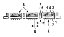
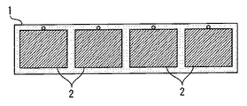
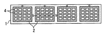
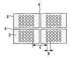
図1は本発明の実施の形態1による半導体装置の表面を示す図であり、図2は図1に示した半導体装置の断面図であり、図3は図1に示した半導体装置の裏面を示す図である。また、図4は図1に示した樹脂封止部を透視した状態を示す図であり、図5は図4のa−a断面図である。また、図6は樹脂封止部の切断部分を示す図であり、図7は半導体装置の裏面の切断部分を示す拡大図であり、図8は切断された半導体装置の断面図である。
【0025】
図1〜図8において、参照符号1は半導体装置用基板(以下「基板」という。)、2は樹脂封止部、3は半田ボール(端子)、4は半導体チップ、5はワイヤ、6は切断部分、7は切り残し部分、8はパッケージ(半導体装置)、11はテストコンタクトピンを示している。
【0026】
先ず、本実施の形態1による半導体装置について説明する。
図1及び図2に示すように、基板1の表面に、複数の樹脂封止部2が形成されている。また、図4及び図5に示すように、樹脂封止部2内には、ワイヤ5によって基板1と電気的に接続された複数の半導体チップ4が設けられている。
【0027】
また、図3及び図5に示すように、基板1の裏面に、樹脂封止部2内の半導体チップ4に対応して、外部電極用の端子としての複数の半田ボール3が形成されている。ここで、隣り合う半導体チップ4(又はパッケージ8)の最も近接する半田ボール3の間隔Aが、半導体チップ4(又はパッケージ8)における半田ボール3の間隔Bのn倍(nは1以上の整数)となるように、半田ボール3が配置されている。例えば、パッケージサイズが0.8mm×0.8mmの場合、間隔Aが9.6mm(=0.8mm×12)であり、間隔Bが0.8mmである。なお、半田ボール3は、半導体チップ4と電気的に接続されたランド(9)を介して形成されている(図17参照)。また、nの値は、通常、2〜20の範囲で設定される。言い換えれば、間隔Aは、間隔Bの2〜20倍に設定される。
また、図5に示すように、半田ボール3の間隔Bと同じ間隔(例えば、0.8mm)でテストコンタクトピン11がグリッド状に配置されている。このテストコンタクトピン11を用いて半導体装置の電気的試験が行われる(後述)。
【0028】
また、図6〜図8に示すように、樹脂封止部2および基板1において隣り合う半導体チップ4の間に、ダイサーによって切断される2つの切断部分6がそれぞれ設けられている。この2つの切断部分6の間、すなわち半導体チップ4(又はパッケージ8)の間の部分が、切り残し部7となる。この切り残し部7は、所望のパッケージサイズに応じて、その大きさが変わる部分である。すなわち、この切り残し部7の大きさを変えることにより、所望のパッケージサイズが得られる。例えば、上記パッケージサイズの場合、切断部分6の幅が0.35mmであり、切り残し部7の幅が0.9mmである。
【0029】
次に、半導体装置の製造方法について説明する。
先ず、図4及び図5に示すように、基板1の表面に複数の半導体チップ4を搭載し、基板1と半導体チップ4とをワイヤ5を用いて電気的に接続する。
次に、複数の半導体チップ4を一括して樹脂封止して、樹脂封止部2を形成する。
【0030】
次に、基板1の裏面に、半導体チップと電気的に接続された複数の半田ボール搭載用ランド(図17参照)を形成する。そして、ランド上に半田ボール3を形成する。ここで、外部電極用の端子として機能するランド及び半田ボール3は、隣り合う半導体チップ4の最も近接する端子の間隔Aが、半導体チップ4における端子の間隔Bのn倍(nは1以上の整数)となるように形成する。例えば、パッケージサイズが8mm×8mmの場合、間隔Aが9.6mm(0.8mm×12)で、間隔Bが0.8mmとなるように、ランドおよび半田ボール3を形成する。
【0031】
次に、基板1上に複数の半導体チップ4が搭載された状態で、且つ複数の半導体チップ4の電気的試験を同時に行う。ここで、電気的試験は、図5に示すように、半田ボール3の間隔Bと同じ間隔(例えば0.8mm)でグリッド状に配置されたテストコンタクトピン11を用いて行う。
【0032】
そして、電気的試験を終了した後、ダイサーによって、樹脂封止部2および基板1に設けられた切断部分6を切断する。ここで、所望のパッケージサイズを得るため、隣り合う半導体チップ4(又はパッケージ8)間に、例えば0.9mm幅の切り残し部7が残るように、それぞれ2回切断する。これにより、パッケージ8が個片化される。
【0033】
以上説明したように、本実施の形態1では、隣り合う半導体チップ4の最も近接する端子(ランド9、半田ボール3)の間隔Aが、半導体チップ4における端子の間隔Bのn倍(nは1以上の整数)となるように、端子の位置を共通化した。このため、半導体チップ4における端子の間隔Bと同じ間隔でグリット状に配置したテストコンタクトピン11を1種類準備すれば、樹脂封止部2内のパッケージサイズが変わった場合でも、同じテストコンタクトピン11で電気的試験を行うことができる。よって、テスト治工具のコストを大幅に削減することができる。
さらに、テスト治工具の交換に要する時間、すなわちパッケージ切替ロスもなくなり、効率的に電気的試験を行うことができる。
【0034】
また、基板状態で複数のパッケージ8(又は半導体チップ4)を同時にテストできるため、電気的試験の生産性が大幅に向上する。さらに、パッケージが小型化した場合でも、電気的試験時や搬送時におけるパッケージの脱落を防止することができる。
【0035】
また、本実施の形態1では、パッケージ8を個片化する際に、切り残し部7を残して、樹脂封止部2および基板1を2回切断することとした。このため、上述のように、端子位置の共通化を図っても、所望のパッケージサイズの半導体装置が得られる。
【0036】
なお、本実施の形態1では、半導体装置用基板としてBGA基板を用いた場合、すなわちBGAタイプのパッケージについて説明したが、これに限られず、LGAタイプのパッケージについても適用することができる。この場合、端子としての半田ボール3を形成しなければよい。
【0037】
【発明の効果】
本発明によれば、半導体装置における端子位置を共通化することによって、半導体装置の電気的試験に用いられる治工具のコストを低減することができる。
【図面の簡単な説明】
【図1】 本発明の実施の形態1による半導体装置の表面を示す図である。
【図2】 図1に示した半導体装置用基板の断面図である。
【図3】 図1に示した半導体装置の裏面を示す図である。
【図4】 図1に示した樹脂封止部を透視した状態を示す図である。
【図5】 図4のa−a断面図である。
【図6】 樹脂封止部の切断部分を示す図である。
【図7】 半導体装置の裏面の切断部分を示す拡大図である。
【図8】 切断された半導体装置の断面図である。
【図9】 従来の半導体装置の表面を示す図である。
【図10】 図9に示した半導体装置の断面図である。
【図11】 図9に示した半導体装置の裏面を示す図である。
【図12】 図9に示した樹脂封止部を透視した状態を示す図である。
【図13】 図12のb−b断面図である。
【図14】 樹脂封止部の切断部分を示す図である。
【図15】 半導体装置の裏面の切断部分を示す拡大図である。
【図16】 切断された半導体装置の断面図である。
【図17】 図16に示した半田ボールの近傍を示す断面図である。
【符号の説明】
1 半導体装置用基板、 2 樹脂封止部、 3 半田ボール、 4 半導体チップ、 5 ワイヤ、 6 切断部分、 7 切り残し部分、 8 パッケージ(半導体装置)、 9 ランド、 11 テストコンタクトピン。[0001]
BACKGROUND OF THE INVENTION
The present invention relates to a semiconductor device and a method for manufacturing the semiconductor device.
[0002]
[Prior art]
In recent years, with the miniaturization of packages, semiconductor devices of BGA (Ball Grid Array) type and LGA (Land Grid Array) type in which external electrodes are arranged in a grid pattern on the entire back surface of a substrate have become widespread.
[0003]
A conventional semiconductor device and a method for manufacturing the semiconductor device will be described below with reference to FIGS.
9 is a view showing the surface of a conventional semiconductor device, FIG. 10 is a cross-sectional view of the semiconductor device shown in FIG. 9, and FIG. 11 is a view showing the back surface of the semiconductor device shown in FIG. 12 is a view showing a state where the resin sealing portion shown in FIG. 9 is seen through, and FIG. 13 is a cross-sectional view taken along the line bb of FIG. 14 is a view showing a cut portion of the resin sealing portion, FIG. 15 is an enlarged view showing a cut portion of the back surface of the semiconductor device, and FIG. 16 is a cross-sectional view of the cut semiconductor device. 17 is a cross-sectional view showing the vicinity of the solder ball shown in FIG.
[0004]
9 to 17,
[0005]
First, a conventional semiconductor device will be described.
As shown in FIGS. 9 and 10, a plurality of resin sealing
[0006]
As shown in FIGS. 12 and 13, a plurality of
Moreover, as shown in FIGS. 14-16, the
[0007]
As shown in FIGS. 15 and 16, in the semiconductor chip 4 (or package 8), a plurality of
[0008]
Next, a method for manufacturing a semiconductor device will be described.
First, a plurality of
Next, the plurality of
Then, solder
[0009]
Next, the
Then, an electrical test of each
[0010]
[Problems to be solved by the invention]
As described above, when performing an electrical test individually, it is necessary to prepare a test tool such as a test contact pin every time the package size is different. For this reason, there has been a problem that the cost of the tool becomes high.
In addition, there is a problem that an electrical test cannot be performed during the time for exchanging the jig for testing, and the electrical test cannot be performed efficiently, that is, a so-called package switching loss occurs.
Further, when the package size is reduced to a CSP (Chip Scale Package), the package becomes too small or too light, and there is a problem that the package falls off during testing or transportation.
[0011]
In order to solve the above problem, the semiconductor chip 4 (or the package 8) is in a state before being singulated, that is, in a state where a plurality of
[0012]
However, the package size is determined by a standardization organization such as JEITA (Japan Electronics and Information Technology Industries Association), but the distance (inter-package pitch) C between the
In addition, even when the package sizes are different, it is necessary to prepare test jigs and tools, and there is a problem that the cost of the jigs cannot be reduced.
Therefore, since the positions of the terminals (for example, solder balls) 3 on the back surface of the
In addition, since the test jig must be replaced, so-called package switching loss cannot be reduced.
[0013]
The present invention has been made to solve the above-described conventional problems, and an object of the present invention is to reduce the cost of a jig used for an electrical test of a semiconductor device by sharing a terminal position in the semiconductor device.
[0014]
[Means for Solving the Problems]
A method of manufacturing a semiconductor device according to the present invention is a substrate having a front surface, a back surface, a first plurality of lands formed on the back surface, and a second plurality of lands formed on the back surface. The interval between the closest portions of the first plurality of lands and the second plurality of lands is an integral multiple of the interval between the closest portions of the first plurality of lands. Preparing a substrate to be
A first semiconductor chip and a second semiconductor chip disposed on a surface of the substrate; electrically connecting the first semiconductor chip and the first plurality of lands; and the second semiconductor chip; Electrically connecting the second plurality of lands;
Forming a resin sealing portion that collectively seals the first semiconductor chip and the second semiconductor chip after electrically connecting the first and second semiconductor chips;
After the resin sealing portion is formed, an electrical test is performed on the first semiconductor chip through the first plurality of lands, and the second semiconductor chip is formed through the second plurality of lands. Conducting an electrical test; and
After performing the electrical test, by forming two cut portions in the substrate and the resin sealing portion between the first plurality of lands and the second plurality of lands, the substrate and Separating the resin sealing portion into a portion including the first semiconductor chip, a portion including the second semiconductor chip, and an uncut portion between the two cut portions. It is a feature.
[0023]
DETAILED DESCRIPTION OF THE INVENTION
Embodiments of the present invention will be described below with reference to the drawings. In the drawings, the same or corresponding parts are denoted by the same reference numerals, and the description thereof may be simplified or omitted.
[0024]
With reference to FIGS. 1-8, the board | substrate for semiconductor devices by
1 is a view showing the surface of the semiconductor device according to the first embodiment of the present invention, FIG. 2 is a cross-sectional view of the semiconductor device shown in FIG. 1, and FIG. 3 is a back view of the semiconductor device shown in FIG. FIG. 4 is a view showing a state where the resin sealing portion shown in FIG. 1 is seen through, and FIG. 5 is a cross-sectional view taken along the line aa in FIG. 6 is a view showing a cut portion of the resin sealing portion, FIG. 7 is an enlarged view showing a cut portion of the back surface of the semiconductor device, and FIG. 8 is a cross-sectional view of the cut semiconductor device.
[0025]
1 to 8,
[0026]
First, the semiconductor device according to the first embodiment will be described.
As shown in FIGS. 1 and 2, a plurality of
[0027]
Further, as shown in FIGS. 3 and 5, a plurality of
Further, as shown in FIG. 5, the test contact pins 11 are arranged in a grid at the same interval (for example, 0.8 mm) as the interval B of the
[0028]
Moreover, as shown in FIGS. 6-8, between the
[0029]
Next, a method for manufacturing a semiconductor device will be described.
First, as shown in FIGS. 4 and 5, a plurality of
Next, the plurality of
[0030]
Next, a plurality of solder ball mounting lands (see FIG. 17) electrically connected to the semiconductor chip are formed on the back surface of the
[0031]
Next, an electrical test of the plurality of
[0032]
And after finishing an electrical test, the cutting
[0033]
As described above, in the first embodiment, the interval A between the nearest terminals (
Furthermore, the time required for replacing the test jig, that is, the package switching loss is eliminated, and the electrical test can be performed efficiently.
[0034]
In addition, since a plurality of packages 8 (or semiconductor chips 4) can be simultaneously tested in the substrate state, the productivity of the electrical test is greatly improved. Furthermore, even when the package is downsized, it is possible to prevent the package from dropping off during electrical testing or transportation.
[0035]
In the first embodiment, when the
[0036]
In the first embodiment, the case where a BGA substrate is used as a semiconductor device substrate, that is, a BGA type package has been described. However, the present invention is not limited to this and can be applied to an LGA type package. In this case, the
[0037]
【The invention's effect】
According to the present invention, by sharing the terminal position in the semiconductor device, the cost of the jig used for the electrical test of the semiconductor device can be reduced.
[Brief description of the drawings]
FIG. 1 is a diagram showing a surface of a semiconductor device according to a first embodiment of the present invention.
2 is a cross-sectional view of the semiconductor device substrate shown in FIG. 1;
FIG. 3 is a view showing a back surface of the semiconductor device shown in FIG. 1;
4 is a view showing a state where a resin sealing portion shown in FIG. 1 is seen through. FIG.
FIG. 5 is a cross-sectional view taken along the line aa in FIG.
FIG. 6 is a view showing a cut portion of a resin sealing portion.
FIG. 7 is an enlarged view showing a cut portion of the back surface of the semiconductor device.
FIG. 8 is a cross-sectional view of a cut semiconductor device.
FIG. 9 is a view showing a surface of a conventional semiconductor device.
10 is a cross-sectional view of the semiconductor device shown in FIG. 9;
11 is a view showing the back surface of the semiconductor device shown in FIG. 9;
12 is a view showing a state where the resin sealing portion shown in FIG. 9 is seen through. FIG.
13 is a cross-sectional view taken along the line bb of FIG.
FIG. 14 is a view showing a cut portion of a resin sealing portion.
FIG. 15 is an enlarged view showing a cut portion of the back surface of the semiconductor device;
FIG. 16 is a cross-sectional view of a cut semiconductor device.
17 is a cross-sectional view showing the vicinity of the solder ball shown in FIG. 16;
[Explanation of symbols]
DESCRIPTION OF
Claims (3)
第1の半導体チップ及び第2の半導体チップを前記基板の表面上に配置し、前記第1の半導体チップと前記第1の複数のランドとを電気的に接続し、前記第2の半導体チップと前記第2の複数のランドとを電気的に接続する工程と、
前記第1及び第2の半導体チップを電気的に接続した後に、前記第1の半導体チップと前記第2の半導体チップとを一括して封止する樹脂封止部を形成する工程と、
前記樹脂封止部を形成した後に、前記第1の複数のランドを介して前記第1の半導体チップに電気的試験を行い、前記第2の複数のランドを介して前記第2の半導体チップに電気的試験を行う工程と、
前記電気的試験を行った後に、前記第1の複数のランドと前記第2の複数のランドとの間の前記基板及び前記樹脂封止部に2つの切断部分を形成することで、前記基板及び前記樹脂封止部を、前記第1の半導体チップを含む部分と、前記第2の半導体チップを含む部分と、前記2つの切断部分の間の切り残し部とに分離する工程とを有することを特徴とする半導体装置の製造方法。And table surface, a substrate having a back surface, a first plurality of lands formed on the back surface, and a second plurality of lands formed on the back surface, said first plurality of lands And preparing a substrate in which the interval between the closest portions of the second plurality of lands is an integral multiple of the interval between the closest portions of the first plurality of lands,
A first semiconductor chip and a second semiconductor chip disposed on a surface of the substrate; electrically connecting the first semiconductor chip and the first plurality of lands; and the second semiconductor chip; Electrically connecting the second plurality of lands;
Forming a resin sealing portion that collectively seals the first semiconductor chip and the second semiconductor chip after electrically connecting the first and second semiconductor chips;
After the resin sealing portion is formed, an electrical test is performed on the first semiconductor chip through the first plurality of lands, and the second semiconductor chip is formed through the second plurality of lands. Conducting an electrical test; and
After performing the electrical test, by forming two cut portions in the substrate and the resin sealing portion between the first plurality of lands and the second plurality of lands, the substrate and Separating the resin sealing portion into a portion including the first semiconductor chip, a portion including the second semiconductor chip, and an uncut portion between the two cut portions. A method of manufacturing a semiconductor device.
前記分離する工程の前に、前記第1の複数のランドと前記第2の複数のランドのそれぞれの上に、半田ボールを形成する工程を更に有することを特徴とする半導体装置の製造方法。In the manufacturing method of the semiconductor device according to claim 1 ,
The method of manufacturing a semiconductor device, further comprising forming a solder ball on each of the first plurality of lands and the second plurality of lands before the separating step.
前記切断部分の形成は、ダイサーによる切断によって行うことを特徴とする半導体装置の製造方法。In the manufacturing method of the semiconductor device according to claim 1 ,
The method of manufacturing a semiconductor device, wherein the cut portion is formed by cutting with a dicer.
Priority Applications (7)
| Application Number | Priority Date | Filing Date | Title |
|---|---|---|---|
| JP2002200930A JP4002143B2 (en) | 2002-07-10 | 2002-07-10 | Manufacturing method of semiconductor device |
| US10/336,801 US7166490B2 (en) | 2002-07-10 | 2003-01-06 | Semiconductor device with terminals, and method of manufacturing the same |
| TW092104639A TW588443B (en) | 2002-07-10 | 2003-03-05 | Semiconductor device, and method of manufacturing the same |
| DE10310536A DE10310536B4 (en) | 2002-07-10 | 2003-03-11 | Semiconductor device and manufacturing method therefor |
| KR10-2003-0015643A KR100536114B1 (en) | 2002-07-10 | 2003-03-13 | Semiconductor device and method of manufacturing the same |
| CNB031199593A CN100378966C (en) | 2002-07-10 | 2003-03-14 | Semiconductor device and manufacturing method thereof |
| US11/473,081 US7348191B2 (en) | 2002-07-10 | 2006-06-23 | Semiconductor device with terminals, and method of manufacturing the same |
Applications Claiming Priority (1)
| Application Number | Priority Date | Filing Date | Title |
|---|---|---|---|
| JP2002200930A JP4002143B2 (en) | 2002-07-10 | 2002-07-10 | Manufacturing method of semiconductor device |
Publications (3)
| Publication Number | Publication Date |
|---|---|
| JP2004047600A JP2004047600A (en) | 2004-02-12 |
| JP2004047600A5 JP2004047600A5 (en) | 2005-10-27 |
| JP4002143B2 true JP4002143B2 (en) | 2007-10-31 |
Family
ID=29997135
Family Applications (1)
| Application Number | Title | Priority Date | Filing Date |
|---|---|---|---|
| JP2002200930A Expired - Fee Related JP4002143B2 (en) | 2002-07-10 | 2002-07-10 | Manufacturing method of semiconductor device |
Country Status (6)
| Country | Link |
|---|---|
| US (2) | US7166490B2 (en) |
| JP (1) | JP4002143B2 (en) |
| KR (1) | KR100536114B1 (en) |
| CN (1) | CN100378966C (en) |
| DE (1) | DE10310536B4 (en) |
| TW (1) | TW588443B (en) |
Families Citing this family (5)
| Publication number | Priority date | Publication date | Assignee | Title |
|---|---|---|---|---|
| JP4002143B2 (en) * | 2002-07-10 | 2007-10-31 | 株式会社ルネサステクノロジ | Manufacturing method of semiconductor device |
| TWI231578B (en) * | 2003-12-01 | 2005-04-21 | Advanced Semiconductor Eng | Anti-warpage package and method for making the same |
| DE102004020187B4 (en) | 2004-04-22 | 2006-07-13 | Infineon Technologies Ag | Redistributable substrate strip with multiple semiconductor device locations |
| KR101010250B1 (en) * | 2009-10-14 | 2011-01-21 | 대건종합건축사사무소 주식회사 | Multi-family housing |
| KR102712511B1 (en) * | 2019-05-10 | 2024-10-07 | 에스케이하이닉스 주식회사 | Method of manufacturing Flip chip package and Test Apparatus of Flip Chips |
Family Cites Families (21)
| Publication number | Priority date | Publication date | Assignee | Title |
|---|---|---|---|---|
| JPS6197941A (en) | 1984-10-19 | 1986-05-16 | Toshiba Corp | Test circuit part in semiconductor wafer |
| JPH0763788A (en) * | 1993-08-21 | 1995-03-10 | Hewlett Packard Co <Hp> | Probe, electrical part / circuit inspecting device and electrical part / method of circuit inspection |
| US5956601A (en) * | 1996-04-25 | 1999-09-21 | Kabushiki Kaisha Toshiba | Method of mounting a plurality of semiconductor devices in corresponding supporters |
| US6284566B1 (en) * | 1996-05-17 | 2001-09-04 | National Semiconductor Corporation | Chip scale package and method for manufacture thereof |
| JPH10135258A (en) | 1996-10-30 | 1998-05-22 | Hitachi Ltd | Multiple wiring board and method of manufacturing semiconductor device using the same |
| US6150193A (en) * | 1996-10-31 | 2000-11-21 | Amkor Technology, Inc. | RF shielded device |
| JPH10256417A (en) * | 1997-03-07 | 1998-09-25 | Citizen Watch Co Ltd | Semiconductor package manufacturing method |
| JPH10284760A (en) * | 1997-04-11 | 1998-10-23 | Oki Electric Ind Co Ltd | Manufacturing method of light receiving and emitting diode array chip |
| JPH1197494A (en) * | 1997-09-18 | 1999-04-09 | Hitachi Ltd | Semiconductor device and manufacturing method thereof |
| US6246250B1 (en) * | 1998-05-11 | 2001-06-12 | Micron Technology, Inc. | Probe card having on-board multiplex circuitry for expanding tester resources |
| JP2000040721A (en) * | 1998-07-22 | 2000-02-08 | Mitsubishi Electric Corp | Test method of chip scale package |
| US6117704A (en) * | 1999-03-31 | 2000-09-12 | Irvine Sensors Corporation | Stackable layers containing encapsulated chips |
| US6251695B1 (en) * | 1999-09-01 | 2001-06-26 | S3 Graphics Co., Ltd. | Multichip module packaging process for known good die burn-in |
| JP2001135658A (en) * | 1999-11-08 | 2001-05-18 | Towa Corp | Method and apparatus for assembling electronic components |
| JP2001144197A (en) * | 1999-11-11 | 2001-05-25 | Fujitsu Ltd | Semiconductor device, method of manufacturing semiconductor device, and method of testing |
| JP2001203293A (en) | 2000-01-18 | 2001-07-27 | Fujitsu Ltd | Method for manufacturing semiconductor device |
| JP3522177B2 (en) | 2000-02-21 | 2004-04-26 | 株式会社三井ハイテック | Method for manufacturing semiconductor device |
| JP2001267492A (en) * | 2000-03-14 | 2001-09-28 | Ibiden Co Ltd | Semiconductor module manufacturing method |
| JP2001298121A (en) | 2000-04-17 | 2001-10-26 | Suzuki Co Ltd | Film for electronic component, its manufacturing method and die to be used therefor |
| JP4475761B2 (en) | 2000-07-26 | 2010-06-09 | 日本テキサス・インスツルメンツ株式会社 | Insulating film for semiconductor package and method for manufacturing the same |
| JP4002143B2 (en) * | 2002-07-10 | 2007-10-31 | 株式会社ルネサステクノロジ | Manufacturing method of semiconductor device |
-
2002
- 2002-07-10 JP JP2002200930A patent/JP4002143B2/en not_active Expired - Fee Related
-
2003
- 2003-01-06 US US10/336,801 patent/US7166490B2/en not_active Expired - Fee Related
- 2003-03-05 TW TW092104639A patent/TW588443B/en not_active IP Right Cessation
- 2003-03-11 DE DE10310536A patent/DE10310536B4/en not_active Expired - Fee Related
- 2003-03-13 KR KR10-2003-0015643A patent/KR100536114B1/en not_active Expired - Fee Related
- 2003-03-14 CN CNB031199593A patent/CN100378966C/en not_active Expired - Fee Related
-
2006
- 2006-06-23 US US11/473,081 patent/US7348191B2/en not_active Expired - Fee Related
Also Published As
| Publication number | Publication date |
|---|---|
| DE10310536A1 (en) | 2004-01-29 |
| US7166490B2 (en) | 2007-01-23 |
| TW588443B (en) | 2004-05-21 |
| US20060240596A1 (en) | 2006-10-26 |
| US20040007783A1 (en) | 2004-01-15 |
| DE10310536B4 (en) | 2006-03-02 |
| US7348191B2 (en) | 2008-03-25 |
| JP2004047600A (en) | 2004-02-12 |
| CN1467830A (en) | 2004-01-14 |
| TW200401415A (en) | 2004-01-16 |
| KR100536114B1 (en) | 2005-12-14 |
| KR20040005573A (en) | 2004-01-16 |
| CN100378966C (en) | 2008-04-02 |
Similar Documents
| Publication | Publication Date | Title |
|---|---|---|
| US8203849B2 (en) | Semiconductor device and manufacture method thereof | |
| JP2982729B2 (en) | Semiconductor device | |
| US20170005030A1 (en) | Flat No-Leads Package With Improved Contact Pins | |
| US6133629A (en) | Multi-chip module package | |
| JP4002143B2 (en) | Manufacturing method of semiconductor device | |
| US6818999B2 (en) | Semiconductor device having multiple semiconductor chips in a single package | |
| KR101013556B1 (en) | Method for fabricating stack package | |
| US7332430B2 (en) | Method for improving the mechanical properties of BOC module arrangements | |
| US8421206B2 (en) | Semiconductor device and connection checking method for semiconductor device | |
| US20030036257A1 (en) | Semiconductor device manufacturing method | |
| JP2008235434A (en) | Semiconductor package | |
| US7868439B2 (en) | Chip package and substrate thereof | |
| US7595255B2 (en) | Method for manufacturing strip level substrate without warpage and method for manufacturing semiconductor package using the same | |
| JP3627238B2 (en) | Semiconductor device and manufacturing method thereof | |
| US6281026B1 (en) | Semiconductor device and method for manufacturing the same | |
| JP3842272B2 (en) | Interposer, semiconductor chip mount sub-board and semiconductor package | |
| JP4030363B2 (en) | Semiconductor device | |
| US6291309B1 (en) | Semiconductor device and method for manufacturing the same | |
| JP4303772B2 (en) | Semiconductor package | |
| JP2001203293A (en) | Method for manufacturing semiconductor device | |
| JP2006080564A (en) | Package structure of semiconductor device | |
| JP2008060159A (en) | Semiconductor device and manufacturing method thereof | |
| JPH11330257A (en) | Semiconductor device and manufacturing method thereof | |
| JP4388989B2 (en) | Semiconductor chip mount sealing sub-board | |
| KR20080023995A (en) | Wafer level flip chip package and method of manufacturing the same |
Legal Events
| Date | Code | Title | Description |
|---|---|---|---|
| A521 | Request for written amendment filed |
Free format text: JAPANESE INTERMEDIATE CODE: A523 Effective date: 20050704 |
|
| A621 | Written request for application examination |
Free format text: JAPANESE INTERMEDIATE CODE: A621 Effective date: 20050704 |
|
| A977 | Report on retrieval |
Free format text: JAPANESE INTERMEDIATE CODE: A971007 Effective date: 20070221 |
|
| A131 | Notification of reasons for refusal |
Free format text: JAPANESE INTERMEDIATE CODE: A131 Effective date: 20070227 |
|
| A521 | Request for written amendment filed |
Free format text: JAPANESE INTERMEDIATE CODE: A523 Effective date: 20070427 |
|
| A131 | Notification of reasons for refusal |
Free format text: JAPANESE INTERMEDIATE CODE: A131 Effective date: 20070522 |
|
| TRDD | Decision of grant or rejection written | ||
| A01 | Written decision to grant a patent or to grant a registration (utility model) |
Free format text: JAPANESE INTERMEDIATE CODE: A01 Effective date: 20070814 |
|
| A61 | First payment of annual fees (during grant procedure) |
Free format text: JAPANESE INTERMEDIATE CODE: A61 Effective date: 20070816 |
|
| FPAY | Renewal fee payment (event date is renewal date of database) |
Free format text: PAYMENT UNTIL: 20100824 Year of fee payment: 3 |
|
| R150 | Certificate of patent or registration of utility model |
Ref document number: 4002143 Country of ref document: JP Free format text: JAPANESE INTERMEDIATE CODE: R150 Free format text: JAPANESE INTERMEDIATE CODE: R150 |
|
| FPAY | Renewal fee payment (event date is renewal date of database) |
Free format text: PAYMENT UNTIL: 20110824 Year of fee payment: 4 |
|
| FPAY | Renewal fee payment (event date is renewal date of database) |
Free format text: PAYMENT UNTIL: 20110824 Year of fee payment: 4 |
|
| S111 | Request for change of ownership or part of ownership |
Free format text: JAPANESE INTERMEDIATE CODE: R313111 |
|
| FPAY | Renewal fee payment (event date is renewal date of database) |
Free format text: PAYMENT UNTIL: 20110824 Year of fee payment: 4 |
|
| R350 | Written notification of registration of transfer |
Free format text: JAPANESE INTERMEDIATE CODE: R350 |
|
| FPAY | Renewal fee payment (event date is renewal date of database) |
Free format text: PAYMENT UNTIL: 20120824 Year of fee payment: 5 |
|
| FPAY | Renewal fee payment (event date is renewal date of database) |
Free format text: PAYMENT UNTIL: 20120824 Year of fee payment: 5 |
|
| FPAY | Renewal fee payment (event date is renewal date of database) |
Free format text: PAYMENT UNTIL: 20130824 Year of fee payment: 6 |
|
| S531 | Written request for registration of change of domicile |
Free format text: JAPANESE INTERMEDIATE CODE: R313531 |
|
| R350 | Written notification of registration of transfer |
Free format text: JAPANESE INTERMEDIATE CODE: R350 |
|
| LAPS | Cancellation because of no payment of annual fees |