JP4004484B2 - 固体撮像素子の製造方法 - Google Patents
固体撮像素子の製造方法 Download PDFInfo
- Publication number
- JP4004484B2 JP4004484B2 JP2004107904A JP2004107904A JP4004484B2 JP 4004484 B2 JP4004484 B2 JP 4004484B2 JP 2004107904 A JP2004107904 A JP 2004107904A JP 2004107904 A JP2004107904 A JP 2004107904A JP 4004484 B2 JP4004484 B2 JP 4004484B2
- Authority
- JP
- Japan
- Prior art keywords
- region
- conductivity type
- type
- insulating film
- gate electrode
- Prior art date
- Legal status (The legal status is an assumption and is not a legal conclusion. Google has not performed a legal analysis and makes no representation as to the accuracy of the status listed.)
- Expired - Fee Related
Links
Images





Classifications
-
- H—ELECTRICITY
- H10—SEMICONDUCTOR DEVICES; ELECTRIC SOLID-STATE DEVICES NOT OTHERWISE PROVIDED FOR
- H10F—INORGANIC SEMICONDUCTOR DEVICES SENSITIVE TO INFRARED RADIATION, LIGHT, ELECTROMAGNETIC RADIATION OF SHORTER WAVELENGTH OR CORPUSCULAR RADIATION
- H10F39/00—Integrated devices, or assemblies of multiple devices, comprising at least one element covered by group H10F30/00, e.g. radiation detectors comprising photodiode arrays
- H10F39/011—Manufacture or treatment of image sensors covered by group H10F39/12
- H10F39/014—Manufacture or treatment of image sensors covered by group H10F39/12 of CMOS image sensors
-
- B—PERFORMING OPERATIONS; TRANSPORTING
- B01—PHYSICAL OR CHEMICAL PROCESSES OR APPARATUS IN GENERAL
- B01D—SEPARATION
- B01D35/00—Filtering devices having features not specifically covered by groups B01D24/00 - B01D33/00, or for applications not specifically covered by groups B01D24/00 - B01D33/00; Auxiliary devices for filtration; Filter housing constructions
- B01D35/30—Filter housing constructions
- B01D35/306—Filter mounting adapter
-
- B—PERFORMING OPERATIONS; TRANSPORTING
- B01—PHYSICAL OR CHEMICAL PROCESSES OR APPARATUS IN GENERAL
- B01D—SEPARATION
- B01D35/00—Filtering devices having features not specifically covered by groups B01D24/00 - B01D33/00, or for applications not specifically covered by groups B01D24/00 - B01D33/00; Auxiliary devices for filtration; Filter housing constructions
- B01D35/14—Safety devices specially adapted for filtration; Devices for indicating clogging
- B01D35/147—Bypass or safety valves
-
- H—ELECTRICITY
- H10—SEMICONDUCTOR DEVICES; ELECTRIC SOLID-STATE DEVICES NOT OTHERWISE PROVIDED FOR
- H10F—INORGANIC SEMICONDUCTOR DEVICES SENSITIVE TO INFRARED RADIATION, LIGHT, ELECTROMAGNETIC RADIATION OF SHORTER WAVELENGTH OR CORPUSCULAR RADIATION
- H10F39/00—Integrated devices, or assemblies of multiple devices, comprising at least one element covered by group H10F30/00, e.g. radiation detectors comprising photodiode arrays
- H10F39/80—Constructional details of image sensors
- H10F39/803—Pixels having integrated switching, control, storage or amplification elements
-
- B—PERFORMING OPERATIONS; TRANSPORTING
- B01—PHYSICAL OR CHEMICAL PROCESSES OR APPARATUS IN GENERAL
- B01D—SEPARATION
- B01D2201/00—Details relating to filtering apparatus
- B01D2201/16—Valves
-
- B—PERFORMING OPERATIONS; TRANSPORTING
- B01—PHYSICAL OR CHEMICAL PROCESSES OR APPARATUS IN GENERAL
- B01D—SEPARATION
- B01D2201/00—Details relating to filtering apparatus
- B01D2201/29—Filter cartridge constructions
-
- B—PERFORMING OPERATIONS; TRANSPORTING
- B01—PHYSICAL OR CHEMICAL PROCESSES OR APPARATUS IN GENERAL
- B01D—SEPARATION
- B01D2201/00—Details relating to filtering apparatus
- B01D2201/34—Seals or gaskets for filtering elements
- B01D2201/347—Radial sealings
Landscapes
- Chemical & Material Sciences (AREA)
- Chemical Kinetics & Catalysis (AREA)
- Solid State Image Pick-Up Elements (AREA)
- Transforming Light Signals Into Electric Signals (AREA)
- Light Receiving Elements (AREA)
Description
ることが可能となる。
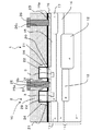
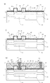
2 光信号検出用のMOSトランジスタ
3 ホールポケット領域
10 単位画素部
11 シリコン基板
12 n型層
13 p型埋め込み層
14 n型層
15 p型ウェル領域
16 n型高濃度拡散領域
16a n型ドレイン領域
16b n型ソース領域
17 ウェル分離領域
20 n型チャネルドープ層
21 ゲート絶縁膜
22 ゲート電極
23 絶縁膜
24 サイドウォール
25 ソース電極
25a、26a、27a コンタクトホール
26 ドレイン電極
28a、28b 画素間分離電極
29 層間絶縁膜
31〜34 マスクパターン
Claims (6)
- 光照射により信号電荷を発生させる受光領域と、該受光領域で発生した信号電荷に応じた信号を出力するトランジスタとをそれぞれ有する複数の単位画素部を二次元のアレイ状に形成する固体撮像素子の製造方法において、
第1導電型基板に形成された第2導電型半導体層上に、該受光領域を構成する第1導電型ウェル領域を形成する工程と、
該第1導電型ウェル領域内に電荷蓄積領域を形成する工程と、
該第1導電型基板の全面にわたってゲート絶縁膜を形成する工程と、
該電荷蓄積領域の上方に該ゲート絶縁膜を介して該トランジスタのゲート電極を形成する工程と、
該ゲート電極下以外のゲート絶縁膜を除去して、該第1導電型基板の表面に熱酸化により絶縁膜を形成する工程と、
該熱酸化した絶縁膜をイオン注入の保護膜とし、かつ該ゲート電極をマスクとして用いて、イオン注入時の平均飛程が該熱酸化した絶縁膜の内部となるように、該第1導電型基板の全面に第2導電型不純物を導入して第2導電型高濃度拡散領域を、該ゲート電極が設けられている領域以外の該第1導電型ウェル領域を含む領域上の基板表層部に形成する工程とを有しており、
該第2導電型高濃度拡散領域として、該第1導電型基板の深さ方向の不純物濃度極大部が該第1導電型基板の表面に形成されている固体撮像素子の製造方法。 - 前記熱酸化した絶縁膜の膜厚を200オングストロームに設定する請求項1に記載の固体撮像素子の製造方法。
- 前記トランジスタはMOSトランジスタである請求項1に記載の固体撮像素子の製造方法。
- 前記第2導電型高濃度拡散領域は、前記第1導電型ウェル領域を含む領域として、該第1導電型ウェル領域上およびその外側を囲む分離領域上において、前記MOSトランジスタのドレイン領域であり、該MOSトランジスタに隣接する分離領域に近接した該第1導電型ウェル領域上において、該MOSトランジスタのソース領域である請求項3に記載の固体撮像素子の製造方法。
- 前記ゲート電極はリング状であって、該リング状の中央穴下の第2導電型高濃度拡散領域が前記ソース領域であり、前記ソース領域の周囲の該ゲート電極下のリング状領域が、前記MOSトランジスタにおける電流担体を移動させるためのチャネル領域である請求項4に記載の固体撮像素子の製造方法。
- 前記第1導電型ウェル領域のうち、前記受光領域を構成する第1導電型ウェル領域上を前記第2導電型高濃度拡散領域によって覆って埋め込み構造とする請求項6に記載の固体撮像素子の製造方法。
Priority Applications (4)
| Application Number | Priority Date | Filing Date | Title |
|---|---|---|---|
| JP2004107904A JP4004484B2 (ja) | 2004-03-31 | 2004-03-31 | 固体撮像素子の製造方法 |
| TW094110370A TWI255040B (en) | 2004-03-31 | 2005-03-31 | Solid-state image sensor and method for fabricating the same |
| KR1020050027134A KR100676284B1 (ko) | 2004-03-31 | 2005-03-31 | 고체 촬상 소자 및 그 제조 방법 |
| US11/096,925 US7304338B2 (en) | 2004-03-31 | 2005-03-31 | Solid-state image sensor and method for fabricating the same |
Applications Claiming Priority (1)
| Application Number | Priority Date | Filing Date | Title |
|---|---|---|---|
| JP2004107904A JP4004484B2 (ja) | 2004-03-31 | 2004-03-31 | 固体撮像素子の製造方法 |
Publications (2)
| Publication Number | Publication Date |
|---|---|
| JP2005294554A JP2005294554A (ja) | 2005-10-20 |
| JP4004484B2 true JP4004484B2 (ja) | 2007-11-07 |
Family
ID=35327143
Family Applications (1)
| Application Number | Title | Priority Date | Filing Date |
|---|---|---|---|
| JP2004107904A Expired - Fee Related JP4004484B2 (ja) | 2004-03-31 | 2004-03-31 | 固体撮像素子の製造方法 |
Country Status (4)
| Country | Link |
|---|---|
| US (1) | US7304338B2 (ja) |
| JP (1) | JP4004484B2 (ja) |
| KR (1) | KR100676284B1 (ja) |
| TW (1) | TWI255040B (ja) |
Families Citing this family (17)
| Publication number | Priority date | Publication date | Assignee | Title |
|---|---|---|---|---|
| WO2005059968A2 (en) * | 2003-12-17 | 2005-06-30 | Analog Devices, Inc. | Integrated circuit fuse and method of fabrication |
| KR101244571B1 (ko) * | 2006-02-22 | 2013-03-26 | 삼성전자주식회사 | 신규한 페로센 함유 고분자 및 이를 이용한 유기 메모리소자 |
| US7642579B2 (en) * | 2006-03-06 | 2010-01-05 | Stmicroelectronics S.A. | Image sensor comprising pixels with one transistor |
| US20080217716A1 (en) * | 2007-03-09 | 2008-09-11 | Mauritzson Richard A | Imaging apparatus, method, and system having reduced dark current |
| US20080258187A1 (en) * | 2007-04-18 | 2008-10-23 | Ladd John W | Methods, systems and apparatuses for the design and use of imager sensors |
| US8257997B2 (en) * | 2007-10-17 | 2012-09-04 | Sifotonics Technologies (Usa) Inc. | Semiconductor photodetectors |
| KR100855403B1 (ko) | 2007-11-27 | 2008-08-29 | 주식회사 동부하이텍 | 이미지센서 및 그 제조방법 |
| KR100855404B1 (ko) | 2007-12-21 | 2008-08-29 | 주식회사 동부하이텍 | 이미지센서 및 그 제조방법 |
| US7833819B2 (en) * | 2008-07-23 | 2010-11-16 | Aptina Imaging Corporation | Method and apparatus for decreasing storage node parasitic charge in active pixel image sensors |
| JP5091886B2 (ja) * | 2009-02-13 | 2012-12-05 | 浜松ホトニクス株式会社 | イメージセンサ |
| JP5271104B2 (ja) * | 2009-02-13 | 2013-08-21 | 浜松ホトニクス株式会社 | リニアイメージセンサ |
| US7977717B1 (en) * | 2009-02-25 | 2011-07-12 | ON Semiconductor Trading, Ltd | Pixel sensing circuit |
| JP6007524B2 (ja) * | 2012-03-12 | 2016-10-12 | セイコーエプソン株式会社 | 固体撮像装置 |
| DE102013018789B4 (de) | 2012-11-29 | 2025-03-06 | Infineon Technologies Ag | Steuern lichterzeugter Ladungsträger |
| US9147710B2 (en) * | 2013-07-23 | 2015-09-29 | Taiwan Semiconductor Manufacturing Co., Ltd. | Photodiode gate dielectric protection layer |
| JP6595750B2 (ja) * | 2014-03-14 | 2019-10-23 | キヤノン株式会社 | 固体撮像装置及び撮像システム |
| JP6892221B2 (ja) * | 2016-03-04 | 2021-06-23 | エイブリック株式会社 | 半導体装置の製造方法 |
Family Cites Families (12)
| Publication number | Priority date | Publication date | Assignee | Title |
|---|---|---|---|---|
| JPS5369526A (en) | 1976-12-03 | 1978-06-21 | Hitachi Ltd | Solid pickup unit |
| JP2002026303A (ja) | 1990-06-25 | 2002-01-25 | Matsushita Electric Ind Co Ltd | 固体撮像装置の製造方法 |
| JP2928058B2 (ja) | 1993-07-15 | 1999-07-28 | 松下電子工業株式会社 | 固体撮像装置の製造方法 |
| JP3516552B2 (ja) | 1996-04-30 | 2004-04-05 | シャープ株式会社 | 受光素子の製造方法 |
| US6051857A (en) * | 1998-01-07 | 2000-04-18 | Innovision, Inc. | Solid-state imaging device and method of detecting optical signals using the same |
| TW494574B (en) | 1999-12-01 | 2002-07-11 | Innotech Corp | Solid state imaging device, method of manufacturing the same, and solid state imaging system |
| JP3664968B2 (ja) | 1999-12-01 | 2005-06-29 | イノテック株式会社 | 固体撮像素子、その製造方法及び固体撮像装置 |
| TW483127B (en) * | 2000-01-07 | 2002-04-11 | Innotech Corp | Solid state imaging device and driving method thereof |
| US6950134B2 (en) * | 2000-02-22 | 2005-09-27 | Innotech Corporation | Method of preventing transfer and storage of non-optically generated charges in solid state imaging device |
| JP2001284568A (ja) * | 2000-03-31 | 2001-10-12 | Sharp Corp | 固体撮像装置 |
| US6448596B1 (en) * | 2000-08-15 | 2002-09-10 | Innotech Corporation | Solid-state imaging device |
| KR20020052791A (ko) | 2000-12-26 | 2002-07-04 | 박종섭 | 기판 표면을 보호할 수 있는 이미지 센서 제조 방법 |
-
2004
- 2004-03-31 JP JP2004107904A patent/JP4004484B2/ja not_active Expired - Fee Related
-
2005
- 2005-03-31 TW TW094110370A patent/TWI255040B/zh not_active IP Right Cessation
- 2005-03-31 US US11/096,925 patent/US7304338B2/en not_active Expired - Fee Related
- 2005-03-31 KR KR1020050027134A patent/KR100676284B1/ko not_active Expired - Fee Related
Also Published As
| Publication number | Publication date |
|---|---|
| TWI255040B (en) | 2006-05-11 |
| US20060086955A1 (en) | 2006-04-27 |
| KR100676284B1 (ko) | 2007-01-30 |
| KR20060045371A (ko) | 2006-05-17 |
| TW200536116A (en) | 2005-11-01 |
| JP2005294554A (ja) | 2005-10-20 |
| US7304338B2 (en) | 2007-12-04 |
Similar Documents
| Publication | Publication Date | Title |
|---|---|---|
| US20220190022A1 (en) | Image sensors | |
| JP3840203B2 (ja) | 固体撮像装置及び固体撮像装置を用いたカメラシステム | |
| JP6541080B2 (ja) | 固体撮像装置 | |
| JP4224036B2 (ja) | フォトダイオード領域を埋め込んだイメージセンサ及びその製造方法 | |
| JP4004484B2 (ja) | 固体撮像素子の製造方法 | |
| JP5100988B2 (ja) | イメージセンサー及びその製造方法 | |
| CN104217987A (zh) | 隔离结构及其形成方法、包括其的图像传感器及制造方法 | |
| US20070045668A1 (en) | Vertical anti-blooming control and cross-talk reduction for imagers | |
| KR20170084519A (ko) | 이미지 센서 | |
| JP4479729B2 (ja) | 固体撮像装置、電子モジュール及び電子機器 | |
| JP3664968B2 (ja) | 固体撮像素子、その製造方法及び固体撮像装置 | |
| JP2005268814A (ja) | 固体撮像装置及び固体撮像装置を用いたカメラシステム | |
| JP5241759B2 (ja) | 固体撮像装置 | |
| US10170515B2 (en) | Implantation process for semiconductor device | |
| JP5478871B2 (ja) | 光電変換装置、撮像システム、及び光電変換装置の製造方法 | |
| CN101388361A (zh) | 制造图像传感器的方法 | |
| JP4435063B2 (ja) | 固体撮像装置及び固体撮像装置を用いたカメラシステム | |
| CN104332481B (zh) | 图像传感器及其形成方法 | |
| KR102026310B1 (ko) | 소자분리구조물 및 그 제조방법, 소자분리구조물을 구비한 이미지 센서 | |
| US20240395842A1 (en) | Image sensor and method of manufacturing the same |
Legal Events
| Date | Code | Title | Description |
|---|---|---|---|
| A977 | Report on retrieval |
Free format text: JAPANESE INTERMEDIATE CODE: A971007 Effective date: 20070216 |
|
| A131 | Notification of reasons for refusal |
Free format text: JAPANESE INTERMEDIATE CODE: A131 Effective date: 20070220 |
|
| A521 | Request for written amendment filed |
Free format text: JAPANESE INTERMEDIATE CODE: A523 Effective date: 20070419 |
|
| A02 | Decision of refusal |
Free format text: JAPANESE INTERMEDIATE CODE: A02 Effective date: 20070514 |
|
| A521 | Request for written amendment filed |
Free format text: JAPANESE INTERMEDIATE CODE: A523 Effective date: 20070612 |
|
| A911 | Transfer to examiner for re-examination before appeal (zenchi) |
Free format text: JAPANESE INTERMEDIATE CODE: A911 Effective date: 20070802 |
|
| TRDD | Decision of grant or rejection written | ||
| A01 | Written decision to grant a patent or to grant a registration (utility model) |
Free format text: JAPANESE INTERMEDIATE CODE: A01 Effective date: 20070821 |
|
| A61 | First payment of annual fees (during grant procedure) |
Free format text: JAPANESE INTERMEDIATE CODE: A61 Effective date: 20070821 |
|
| R150 | Certificate of patent or registration of utility model |
Free format text: JAPANESE INTERMEDIATE CODE: R150 |
|
| FPAY | Renewal fee payment (event date is renewal date of database) |
Free format text: PAYMENT UNTIL: 20100831 Year of fee payment: 3 |
|
| FPAY | Renewal fee payment (event date is renewal date of database) |
Free format text: PAYMENT UNTIL: 20110831 Year of fee payment: 4 |
|
| FPAY | Renewal fee payment (event date is renewal date of database) |
Free format text: PAYMENT UNTIL: 20110831 Year of fee payment: 4 |
|
| FPAY | Renewal fee payment (event date is renewal date of database) |
Free format text: PAYMENT UNTIL: 20120831 Year of fee payment: 5 |
|
| LAPS | Cancellation because of no payment of annual fees |