JP4017204B2 - Solid-state radiation imaging equipment - Google Patents
Solid-state radiation imaging equipment Download PDFInfo
- Publication number
- JP4017204B2 JP4017204B2 JP22574396A JP22574396A JP4017204B2 JP 4017204 B2 JP4017204 B2 JP 4017204B2 JP 22574396 A JP22574396 A JP 22574396A JP 22574396 A JP22574396 A JP 22574396A JP 4017204 B2 JP4017204 B2 JP 4017204B2
- Authority
- JP
- Japan
- Prior art keywords
- shielding
- pixel
- line
- lines
- array pattern
- Prior art date
- Legal status (The legal status is an assumption and is not a legal conclusion. Google has not performed a legal analysis and makes no representation as to the accuracy of the status listed.)
- Expired - Fee Related
Links
Images


Classifications
-
- H—ELECTRICITY
- H10—SEMICONDUCTOR DEVICES; ELECTRIC SOLID-STATE DEVICES NOT OTHERWISE PROVIDED FOR
- H10F—INORGANIC SEMICONDUCTOR DEVICES SENSITIVE TO INFRARED RADIATION, LIGHT, ELECTROMAGNETIC RADIATION OF SHORTER WAVELENGTH OR CORPUSCULAR RADIATION
- H10F39/00—Integrated devices, or assemblies of multiple devices, comprising at least one element covered by group H10F30/00, e.g. radiation detectors comprising photodiode arrays
- H10F39/10—Integrated devices
- H10F39/12—Image sensors
- H10F39/18—Complementary metal-oxide-semiconductor [CMOS] image sensors; Photodiode array image sensors
-
- H—ELECTRICITY
- H10—SEMICONDUCTOR DEVICES; ELECTRIC SOLID-STATE DEVICES NOT OTHERWISE PROVIDED FOR
- H10F—INORGANIC SEMICONDUCTOR DEVICES SENSITIVE TO INFRARED RADIATION, LIGHT, ELECTROMAGNETIC RADIATION OF SHORTER WAVELENGTH OR CORPUSCULAR RADIATION
- H10F39/00—Integrated devices, or assemblies of multiple devices, comprising at least one element covered by group H10F30/00, e.g. radiation detectors comprising photodiode arrays
- H10F39/80—Constructional details of image sensors
- H10F39/805—Coatings
- H10F39/8057—Optical shielding
Landscapes
- Solid State Image Pick-Up Elements (AREA)
- Transforming Light Signals Into Electric Signals (AREA)
- Light Receiving Elements (AREA)
- Measurement Of Radiation (AREA)
- Apparatus For Radiation Diagnosis (AREA)
Description
【0001】
【発明の属する技術分野】
本発明は一般に固体放射線イメージング装置に関するものであり、更に詳しくはこのような固体放射線イメージング装置で幻影(phantom)ノイズおよび画像アーチファクトを低減するための構造に関するものである。
【0002】
【従来の技術】
固体放射線イメージング装置は典型的には、行および列に配列された複数の画素を有する大形のフラットパネル・イメージング装置を含む。各画素は、スイッチング・トランジスタを介して2つの別個のアドレス線(すなわち、走査線およびデータ線)に結合された光センサ(例えば、ホトダイオード)を含む。各々の画素行では、各々のスイッチング・トランジスタ、典型的には薄膜電界効果トランジスタ(FET)のゲート電極が共通の走査線に結合される。各々の画素列では、各々のトランジスタの読出し電極(例えば、FETのソース電極)がデータ線に結合される。動作の際、放射線(例えば、X線束)がパルス式にオン状態にされ(すなわち供給され)、被検体を通過したX線がイメージング配列に入射する。放射線はシンチレータ材に入射し、画素の光センサがX線とシンチレータとの相互作用によって発生する光の量を(ダイオードを横切る電荷の変化により)測定する。この代わりに、X線で直接に光センサに電子正孔対を発生させることもできる(これは通常、「直接検出」と呼ばれる)。このような光センサの電荷データを読み出すには、各々の画素行を順次に駆動し(すなわち、走査線に信号を印加して、その走査線に結合されたスイッチング・トランジスタを導電状態にし)、それぞれの駆動された画素から信号をそれぞれのデータ線を介して読み出す(すなわち、導電状態のスイッチング・トランジスタとそのデータ線に結合された対応する読出し電極とを介して、ホトダイオードの電荷信号がデータ線に結合される)。このように、画素に結合された走査線の駆動と、その画素に結合されたデータ線からの読出しとの組み合わせにより、所与の画素をアドレス指定することができる。
【0003】
フラットパネル・イメージング装置の性能は、データ線と画素ホトダイオード電極との間の容量結合により劣化する。詳しく述べると、通常のイメージング装置の動作では、画素の読出しの間、X線束はオン状態に留まっている。このような動作の一例は、手術または携帯用に使用される可能性のある小形の装置またはあまり複雑でない装置によるX線透視の場合である。このような装置は軽量で低コストのX線発生器を使用しており、このX線発生器は適当な出力信号を作成するために、連続的にオン状態にしなければならない。更に一般的に、このような装置は、読出し期間の間の放射を防止するために関連の期間の間にX線ビームをオンとオフに素早く繰り返し切り換えるように構成されていない。もう1つの例は、放射線療法に使用されるイメージング装置であり、このイメージング装置では、放射線源が(伝達される線量を最大にするため)連続的にオン状態にされるかまたは、周期的にパルス式にオン状態にされる。これらのパルスは読出し期間の間に生じ得る。このように画素を読み出しながら同時にイメージング装置を励起すると、画像アーチファクトまたは「幻影(phantom)」画像が生じる。幻影画像は、それぞれのホトダイオード電極と隣接のデータ線との間の容量結合の結果として生じる。所与のデータ線に結合された所与の画素の読出しの間、他の画素電極(例えば、読み出されない画素)の電位は、放射線束がイメージング装置に当たるので変化し続ける。読出し中でない画素の電位の変化はデータ線に容量結合され、これにより付加的な電荷が誘起される。この付加的な電荷は、増幅器により読み出され、アドレス指定された画素からの信号の一部として供給される。この影響により、画像に漏話またはコントラストの劣化が生じる。この影響は一般に、表示の中の明るい線として見られる。
【0004】
【発明が解決しようとする課題】
漏話が最小であるとともに、X線束が印加されている間に画素が読み出される動作モードを含む多数の動作モードで安定で正確な画像を発生することができる固体イメージング装置を提供することが望ましい。
【0005】
【課題を解決しようとする手段】
本発明では、画素のホトダイオードと読出しデータ線との間の容量結合を低減し、したがって幻影画像または画像アーチファクトを低減する固体放射線イメージング装置が提供され、このイメージング装置は、走査線および関連するスイッチング・トランジスタのゲート電極の両者と同じ装置内レベル(すなわち、装置の中の同じ高さの所)に配置された複数の遮蔽線を含む。遮蔽線は、データ線と同じ軸に沿った方向に伸び、且つそれぞれの画素のホトダイオードの部分とデータ線の隣接部分との間に配置されたそれぞれの画素遮蔽用枝部分を含む。遮蔽線は、遮蔽線ギャップ距離だけデータ線の隣接部分から離れている。遮蔽線は一般的には母線部分を含む。この母線部分は走査線と同じ軸に沿った方向に伸びるか、またはその代わりにデータ線の軸に沿った方向に伸び、遮蔽線の枝部分は母線部分から伸びる。遮蔽線が共通電位に維持されるように、遮蔽線は典型的には遮蔽電圧源に結合される。遮蔽線は典型的には走査線と同じ導電性材料で構成され、イメージング装置の製造工程の間に、走査線の導電性材料の堆積およびパターン形成と同時に製造される。
【0006】
新規性があると考えられる本発明の特徴は、特許請求の範囲に明確に述べられている。しかし添付の図面を参照した以下の説明により、本発明自体の構成および動作方法は、本発明の上記以外の目的および利点とともに、最も良く理解することができよう。全図を通じて、同じ参照番号は同じ部品を表す。
【0007】
【発明の詳しい説明】
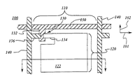
固体放射線イメージング装置100は、行および列から成るマトリクス状のイメージング配列パターンとして配列された複数の画素110(その内の代表的な1つの画素が図1に示されている)を含む。イメージング装置100は第1の軸101および第2の軸102(これらは説明のためのもので、限定するものではない)を有する。第1の軸101はそれに沿って画素の行がそろえられる軸であり、第2の軸102はそれに沿って画素の列がそろえられる軸である。各画素110には、光センサ120および薄膜スイッチング・トランジスタ130が含まれる。光センサ120は一般的にホトダイオードで構成され、その能動領域(すなわち、光電性領域)と一致する画素電極122を有する。スイッチング・トランジスタ130は一般的に、ゲート電極132、ドレーン電極134、およびソース電極すなわち読出し電極136を有する薄膜電界効果トランジスタ(FET)で構成される。イメージング装置100は更に、複数のデータ線140および走査線150も含む。イメージング配列パターン内の各々の画素行に対して第1の軸101に沿って、少なくとも1つの走査線150が配置される。各走査線は、その画素行の中の画素のそれぞれのゲート電極132に結合される。イメージング配列パターン内の各々の画素列に対して第2の軸102に沿って、少なくとも1つのデータ線が配置される。このデータ線は、その画素行の中の画素のそれぞれの読出し電極136に結合される。
【0008】
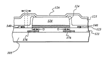
1つの画素110の部分的な横断面図が図2に示されている。ホトダイオード120は基板105の上方に配置される。説明を容易にするため、画素電極122と基板105との間には複数の誘電体層がされ得るが、図には包括的に第1の誘電体層121として示されている。ホトダイオードは光電性物質体124(典型的にはアモルファス・シリコンより成る)を含み、光電性物質体124は、イメージング配列の上に配置される共通電極126(典型的には酸化インジウム錫より成る)に電気的に結合される。窒化シリコンなどより成る第2の誘電体層123が、光電性物質体124の側壁の一部をおおって伸びる。ポリイミドなどより成る第3の誘電体層125が、イメージング配列内の共通電極126と他の構成要素との間に配置される(第2の誘電体層123および第3の誘電体層125の中のバイア(via)を介した光電性物質体124に対するコンタクトを除く)。
【0009】
図2に示されるようなイメージング配列には、配列内の導電性構成要素相互間に容量結合の数個の源がある。例えば、各データ線140と隣接の画素電極122との間に容量結合がある。本明細書中で使用される用語、「隣接」の導電性構成要素とは、空間的に互いに接近しているが、物理的に直接接触していない構成要素であって、したがってその2つの構成要素の間に直接の導電性経路(すなわち短絡)が存在しないような構成要素を指す。解析のため、データ線と隣接のホトダイオードのベース電極との間の結合は2つの静電容量に分解される。その第1の静電容量C10(説明のために図2に破線で表してあり、配列内の個別のコンデンサ構成要素を表すものではない)は、主として、基板と画素電極122の下に配置された物質とを介した結合を表す。(ここで、本明細書で使用される用語「下」、「上方」、「上」等は基板に対する構成要素の相対位置を表すために使用されるもので、イメージング配列の配置方向、使用、または動作に対するどのような制約も意味するものではないことに留意されたい)。第2の静電容量C20は、ベース電極122より上の配列要素を介した容量結合を表す。「下方の経路」の静電容量C10は、「上方の経路」の静電容量C20に比べて、誘起静電容量に対する寄与が大きくなることが多いということが観測された。他の容量結合の源は、画素電極122と共通電極126との間(図2にC21で表されている)、およびデータ線140と共通電極126との間(図2にC22で表されている)にある。(一般的には小さい走査線の寄生静電容量を除いた)総画素静電容量Cpxは次式で表される。
【0010】
Cpx=2(C10+C20)+C21
画素電極の面積がデータ線の面積よりずっと大きいので、CpxはC21(ベース電極と共通電極との間の静電容量)により支配される。総画素静電容量は画素の両側のデータ線に対する誘起静電容量の関数であり、したがってC10とC20との和が2倍される。
【0011】
容量結合効果は、画素の読出しを行っている時間のすべてまたは一部の間にイメージング装置が励起される(すなわち、当該放射線(例えばX線)がイメージング装置に入射する)動作において重要であることが最も多い。イメージング装置が励起される期間の間に読み出される信号は、イメージング装置が励起されない期間の間に読み出される信号より大きくなる。平均信号に対して正規化された増加の1つの近似は、次のように表すことができる。
【0012】
【数1】
2[(C10+C20)/Cpx]×Z1 ×Z2
ここで、Z1 ≡[(読出しチャネル当たりの画素数)/(放射線ビームに照射された画素の走査線の数)]、Z2 ≡[(積分時間)/(線走査時間)]。
式(C10+C20)は、単一の画素電極と1つの隣接のデータ線との間の結合静電容量を表す。配列のレイアウトでは、各データ線140は一般的に、2つの画素電極122に隣接する。線走査時間に対する増幅器の積分時間の比は比較的小さく、約0.85である。連続透視検査またはパルス状透視検査では、X線ビーム・オン時間がフレーム間時間のかなりの部分であれば、結合効果の大きさは2[(C10+C20)/Cpx]である。この比により、容量性結合効果の大きさを明らかにする有用な方法が得られる。図1および図2を参照して説明した構成を有するイメージング装置の場合には、構造から計算した、またはイメージング装置データから推定した2[(C10+C20)/Cpx]の値は約0.5%の範囲にある。この値はかなり大きい。それは、X線イメージング装置における代表的なコントラスト変調が約0.1%から約10%までの範囲内にあるからである。
【0013】
本発明によれば放射線イメージング装置100に、複数の遮蔽線170(図3および図4)を設ける。遮蔽線170は、画素電極122と隣接のデータ線140との間の容量性結合を小さくするように配置される。遮蔽線170は基板105の上方の第1のレベル172に配置される。この第1のレベルは、基板105の上方に配置される走査線150のレベルと同じレベルである。典型的には、遮蔽線170は、走査線と同じ導電性材料(例えば、モリブデン、クロム、チタン等)で構成され、遮蔽線170は同じ金属堆積およびパターン形成工程で走査線と同時に形成される(したがって、製造プロセスに余分な工程が付加されることはない)。遮蔽線170を設けた本発明の構造により、それぞれの画素電極122とデータ線140との間に遮蔽効果が得られるので、これらの構成要素の間に誘起される静電容量は小さくなる。特に、画素電極の下のレベルに遮蔽線を位置決めすることにより、誘起される静電容量値C10(図2に示されるような「下方の経路」の静電容量)が小さくなる。アース平面電極を使用して誘起される静電容量を小さくするもう1つの手法が、本出願人による1995年9月5日出願の米国特許出願第08/523,324号に示されている。
【0014】
各遮蔽線170は母線部分174を含み、この母線部分174から、画素電極122と隣接データ線部分140との間に配置されるようにそれぞれの画素遮蔽用枝部分176が伸びる。図3に示される本発明の一実施例では、遮蔽線の母線部分174は画素110の行に平行な第1の軸101に沿ってそろえられる。この代わりに、遮蔽線の母線部分174は画素110の列に平行な第2の軸102に沿った方向に伸びるようにする。
【0015】
画素遮蔽用枝部分176は、データ線140の隣接部分から遮蔽線ギャップ距離Gだけ離れるように配置される。この距離は約2μmから約20μmまでの範囲にあり、典型的には約5μmである(図3に示すようにギャップ距離Gは、データ線140の部分から遮蔽線170を隔てている最短の横方向距離部分である)。遮蔽線ギャップ距離の最小値は一般に、プロセス手法(例えば、写真印刷プロセス)、およびイメージング装置で導電性の構造を確実に製造することができる分解能によって制限される。最大距離は充てん係数、およびホトダイオードの能動領域を含む配列領域の部分の最適化に関する配慮によって決められる。
【0016】
本発明の一実施例では、図3および図4に示すように、画素電極122のどの部分の下に位置しないように遮蔽線170が配置される。図5に示されるような本発明の代替実施例では、遮蔽線170はオーバラップ距離Dだけ画素電極122の下に伸びる。オーバラップ距離Dは一般的に、約1μmから約20μmまでの範囲にある。したがって遮蔽線の枝部分の幅は、オーバラップ距離Dの大きさに応じて、約2μmから約50μmまで変わり得る。
【0017】
モデル解析では図3および図4に示される遮蔽線構造は、比較的小さな遮蔽線ギャップ距離、例えば約5μm未満で距離で静電容量を小さくするのに非常に有効である。(図3および図4に示される構造に類似した構造を有する装置に基づく)このような解析により、データ線140と画素電極122との間の静電容量は、ギャップ距離が約2μmの場合には約0.1pF/cmの値から約0.06pF/cmの値へと小さくなり、ギャップ距離が約5μmの場合にはデータ線140と画素電極122との間の静電容量は約0.09pF/cmの値から約0.05pF/cmの値へと小さくなる。
【0018】
画素電極122の下に遮蔽線170の一部分を配置することは、データ線140と画素電極122との間の静電容量を小さくする上での遮蔽線170の有効性を高める役目を果たす。典型的には、ギャップ距離が約5μmの場合、該静電容量は約0.1pF/cmの値から約0.001pF/cmの値へ減少する。
遮蔽線170は更に遮蔽共通電圧源190(図3)に結合される。遮蔽共通電圧源190は、アドレス指定されている画素のまわりに配置された遮蔽線(およびそれに取り付けられた遮蔽線枝部分)を固定電位に維持する。図3に示される構成では、イメージング配列の動作中、すべての遮蔽線が同じ一定電位に維持されるように、各遮蔽線は電圧源190に結合される。遮蔽線の存在は画素電極122とデータ線140との間の電界線を乱す傾向があるので、イメージング配列のそれらの2つの構成要素の間の静電容量を小さくする。上記の代りの実施例では、遮蔽共通電圧源190がイメージング配列の共通電極126に対して使用されるのと同じ電圧源で構成され、遮蔽線がバイア(via)177を介して共通電極126に結合される。(バイア177の代表的な1つが図3に示されている。説明を容易にするため、1つの図に相異なる代替実施例をしているが、所与のイメージング配列では一般的に1つの形式の接続構造だけが使用されることに留意されたい。)バイア177はイメージング配列中に設けられて、イメージング配列の第1のレベルの遮蔽線170とホトダイオード構造の上方に配置された共通電極材(典型的には、酸化インジウムスズ)との間の導電性の経路を提供する。代替実施例では、遮蔽線170を隣接する画素の走査線150に結合して(図示しない)、所与の画素行に対する遮蔽線が他の1つの画素行、典型的には次の隣接の画素行に対する走査線と同じ電位に維持されるようにすることが出来る。このようにして、画素の特定の行がアドレス指定されている間、遮蔽線が一定の電位に保持される。遮蔽線が結合されている走査線がアドレス指定されるとき、遮蔽線は電位の変化を受けるが、そのときその遮蔽線により遮蔽されるその特定の画素行はアドレス指定されていない。
【0019】
このように本発明の遮蔽線構造は、データ線と画素電極との間に誘起される静電容量を小さくすることによりイメージング装置の性能を向上する。
以上、本発明を図示し説明してきたが、熟練した当業者には明らかなように、本発明の趣旨および範囲を逸脱することなく、開示された実施例に対して変形および変更を加えることができる。したがって、本発明の趣旨の中に入るこのような変形および変更をすべて包含するように特許請求の範囲を記述してあることが理解されるはずである。
【図面の簡単な説明】
【図1】従来技術によるイメージング装置の配列の一部の平面図である。
【図2】図1の線I−Iに沿って見た代表的な画素の部分横断面図である。
【図3】本発明の一実施例による遮蔽線を設けたイメージング装置の配列の平面図である。
【図4】図3の線II−IIに沿って見た代表的な画素の部分横断面図である。
【図5】本発明の他の1つの実施例による代表的な画素の部分横断面図である。
【符号の説明】
100 固体放射線イメージング装置
101 第1の軸
102 第2の軸
105 基板
110 画素
120 光センサ
121 第1の誘電体層
122 画素電極
123 第2の誘電体層
124 光電性物質体
125 第3の誘電体層
126 共通電極
130 薄膜スイッチング・トランジスタ
132 ゲート電極
134 ドレーン電極
136 読出し電極
140 データ線
150 走査線
170 遮蔽線
174 遮蔽線の母線部分
176 遮蔽線の画素遮蔽用枝部分
G 遮蔽線ギャップ距離[0001]
BACKGROUND OF THE INVENTION
The present invention relates generally to solid state radiation imaging devices, and more particularly to a structure for reducing phantom noise and image artifacts in such solid state radiation imaging devices.
[0002]
[Prior art]
Solid state radiation imaging devices typically include large flat panel imaging devices having a plurality of pixels arranged in rows and columns. Each pixel includes a photosensor (e.g., a photodiode) that is coupled to two separate address lines (i.e., scan lines and data lines) via switching transistors. In each pixel row, the gate electrode of each switching transistor, typically a thin film field effect transistor (FET), is coupled to a common scan line. In each pixel column, the read electrode of each transistor (eg, the source electrode of the FET) is coupled to the data line. In operation, radiation (eg, X-ray flux) is pulsed on (ie, supplied) and X-rays that have passed through the subject enter the imaging array. Radiation is incident on the scintillator material and the pixel photosensor measures the amount of light generated by the interaction of the x-rays and the scintillator (by changing the charge across the diode). Alternatively, electron-hole pairs can be generated directly in the photosensor with X-rays (this is usually referred to as “direct detection”). To read out the charge data of such a photosensor, each pixel row is driven sequentially (ie, a signal is applied to the scan line to make the switching transistor coupled to that scan line conductive) A signal is read from each driven pixel via a respective data line (ie, a photodiode charge signal is transferred to the data line via a conductive switching transistor and a corresponding read electrode coupled to the data line). To be combined). Thus, a given pixel can be addressed by a combination of driving a scan line coupled to a pixel and reading from a data line coupled to that pixel.
[0003]
The performance of flat panel imaging devices is degraded by capacitive coupling between the data lines and the pixel photodiode electrodes. Specifically, in normal imaging device operation, the X-ray flux remains on during pixel readout. An example of such an operation is the case of fluoroscopy with a small or less complex device that may be used for surgery or portable. Such devices use a light, low cost x-ray generator that must be continuously turned on to produce a suitable output signal. More generally, such devices are not configured to quickly and repeatedly switch the x-ray beam on and off during the relevant period to prevent radiation during the readout period. Another example is an imaging device used for radiation therapy, where the radiation source is turned on continuously (to maximize the dose delivered) or periodically It is turned on in a pulsed manner. These pulses can occur during the readout period. Exciting the imaging device at the same time as reading out pixels in this way produces image artifacts or “phantom” images. A phantom image results from capacitive coupling between each photodiode electrode and an adjacent data line. During readout of a given pixel coupled to a given data line, the potential of other pixel electrodes (eg, pixels that are not read out) continues to change as the radiation flux strikes the imaging device. Changes in the potential of the pixels not being read are capacitively coupled to the data lines, thereby inducing additional charges. This additional charge is read by the amplifier and supplied as part of the signal from the addressed pixel. This effect causes crosstalk or contrast degradation in the image. This effect is generally seen as a bright line in the display.
[0004]
[Problems to be solved by the invention]
It would be desirable to provide a solid-state imaging device with minimal crosstalk and capable of generating stable and accurate images in a number of operating modes, including those in which pixels are read out while an x-ray flux is applied.
[0005]
[Means to solve the problem]
In the present invention, a solid state radiation imaging device is provided that reduces capacitive coupling between a photodiode of a pixel and a readout data line, and thus reduces phantom images or image artifacts, the imaging device comprising a scan line and an associated switching line. It includes a plurality of shielding lines located at the same in-device level (ie, at the same height in the device) as both of the transistor gate electrodes. The shielding line includes a pixel shielding branch portion extending in the direction along the same axis as the data line and disposed between the photodiode portion of each pixel and the adjacent portion of the data line. The shield line is separated from the adjacent portion of the data line by the shield line gap distance. The shielding line generally includes a busbar portion. The bus line portion extends in the direction along the same axis as the scan line, or alternatively extends in the direction along the data line axis, and the branch portion of the shield line extends from the bus line portion. The shield line is typically coupled to a shield voltage source so that the shield line is maintained at a common potential. The shield line is typically composed of the same conductive material as the scan line and is manufactured simultaneously with the deposition and patterning of the scan line conductive material during the manufacturing process of the imaging device.
[0006]
The features of the invention believed to be novel are set forth with particularity in the appended claims. However, from the following description with reference to the accompanying drawings, the structure and operation method of the present invention, together with other objects and advantages of the present invention, can be best understood. Like reference numerals refer to like parts throughout the drawings.
[0007]
Detailed Description of the Invention
The solid-state
[0008]
A partial cross-sectional view of one
[0009]
In an imaging array such as that shown in FIG. 2, there are several sources of capacitive coupling between conductive components in the array. For example, there is capacitive coupling between each
[0010]
C px = 2 (C10 + C20) + C21
Since the area of the pixel electrode is much larger than the area of the data line, C px is dominated by C21 (capacitance between the base electrode and the common electrode). The total pixel capacitance is a function of the induced capacitance for the data lines on both sides of the pixel, so the sum of C10 and C20 is doubled.
[0011]
Capacitive coupling effects are important in operations where the imaging device is excited (ie, the radiation (eg, x-rays) is incident on the imaging device) during all or part of the time during which the pixel is being read out Is the most common. The signal read during the period when the imaging device is excited is larger than the signal read during the period when the imaging device is not excited. One approximation of the increase normalized to the average signal can be expressed as:
[0012]
[Expression 1]
2 [(C10 + C20) / C px ] × Z 1 × Z 2
Here, Z 1 ≡ [(number of pixels per readout channel) / (number of scanning lines of pixels irradiated with radiation beam)], Z 2 ≡ [(integration time) / (line scanning time)].
Equation (C10 + C20) represents the combined capacitance between a single pixel electrode and one adjacent data line. In the array layout, each
[0013]
According to the present invention, the
[0014]
Each
[0015]
The pixel shielding
[0016]
In one embodiment of the present invention, as shown in FIGS. 3 and 4, the
[0017]
In model analysis, the shield line structure shown in FIGS. 3 and 4 is very effective in reducing capacitance at relatively small shield line gap distances, eg, distances below about 5 μm. According to such an analysis (based on a device having a structure similar to the structure shown in FIGS. 3 and 4), the capacitance between the
[0018]
Arranging a part of the
[0019]
As described above, the shielding line structure of the present invention improves the performance of the imaging apparatus by reducing the capacitance induced between the data line and the pixel electrode.
While the invention has been illustrated and described, as will be apparent to those skilled in the art, changes and modifications may be made to the disclosed embodiments without departing from the spirit and scope of the invention. it can. Therefore, it should be understood that the appended claims have been written to cover all such variations and modifications that fall within the spirit of the invention.
[Brief description of the drawings]
FIG. 1 is a plan view of a portion of an array of imaging devices according to the prior art.
FIG. 2 is a partial cross-sectional view of a representative pixel as viewed along line II in FIG.
FIG. 3 is a plan view of an array of imaging devices provided with shielding lines according to an embodiment of the present invention.
4 is a partial cross-sectional view of a representative pixel viewed along line II-II in FIG. 3. FIG.
FIG. 5 is a partial cross-sectional view of an exemplary pixel according to another embodiment of the present invention.
[Explanation of symbols]
100 Solid-State
Claims (4)
行および列から成るイメージング配列パターンに配置された複数の画素であって、当該画素の各々が薄膜スイッチング・トランジスタに結合された光センサを有している複数の画素、
上記イメージング配列パターンの第1の軸に沿って上記基板に対する第1のレベルに配置された複数の走査線であって、上記イメージング配列パターン内の各々の画素行に対してそれぞれの走査線が設けられ、それぞれの走査線の各々が、上記イメージング配列パターン内のそれぞれの画素行に沿って配置された画素の各々に対する上記スイッチング・トランジスタのそれぞれのゲート電極に結合されている複数の走査線、
上記イメージング配列パターンの第2の軸に沿って上記基板に対する第2のレベルに配置された複数のデータ線であって、上記イメージング配列パターン内の各々の画素列に対してそれぞれのデータ線が設けられ、それぞれのデータ線の各々が、上記イメージング配列パターン内のそれぞれの画素列に沿って配置された画素の各々に対する上記スイッチング・トランジスタのそれぞれの読出し電極に結合されている複数のデータ線、および
上記基板に対する上記第1のレベルに配置される複数の遮蔽線であって、当該遮蔽線の各々が、上記画素の一部分と上記データ線の隣接部分との間に上記第2の軸に沿って配置されたそれぞれの画素遮蔽用枝部分を有している複数の遮蔽線を含んでおり、
上記画素遮蔽用枝部分は、上記データ線の隣接部分から前記第1の軸の方向に遮蔽線ギャップ距離だけ離れており、
上記イメージング配列パターン内に配置された前記複数の遮蔽線は、遮蔽共通電圧源に結合され、該複数の遮蔽線が同じ一定電位に維持されることを特徴とする固体放射線イメージング装置。In a solid-state radiation imaging device for producing an image with low image artifacts during imaging device readout, wherein the components are located at a level above the substrate,
A plurality of pixels arranged in an imaging array pattern of rows and columns, each pixel having a photosensor coupled to a thin film switching transistor;
A plurality of scan lines arranged at a first level relative to the substrate along a first axis of the imaging array pattern, each scan line being provided for each pixel row in the imaging array pattern A plurality of scan lines, each of which is coupled to a respective gate electrode of the switching transistor for each of the pixels disposed along a respective pixel row in the imaging array pattern;
A plurality of data lines arranged at a second level relative to the substrate along a second axis of the imaging array pattern, each data line being provided for each pixel column in the imaging array pattern A plurality of data lines each coupled to a respective readout electrode of the switching transistor for each of the pixels disposed along a respective pixel column in the imaging array pattern; and a plurality of shielding lines that will be placed on the first level for the substrate, each of the shielding lines, along the second axis between a portion and the adjacent portions of the data lines of the pixel Including a plurality of shielding lines each having a pixel shielding branch portion disposed;
The pixel shielding branch portion is separated from the adjacent portion of the data line by a shielding line gap distance in the direction of the first axis,
The plurality of shielding lines arranged in the imaging array pattern are coupled to a shielding common voltage source, and the plurality of shielding lines are maintained at the same constant potential.
Applications Claiming Priority (2)
| Application Number | Priority Date | Filing Date | Title |
|---|---|---|---|
| US08/523323 | 1995-09-05 | ||
| US08/523,323 US5610403A (en) | 1995-09-05 | 1995-09-05 | Solid state radiation imager with gate electrode plane shield wires |
Publications (2)
| Publication Number | Publication Date |
|---|---|
| JPH09171080A JPH09171080A (en) | 1997-06-30 |
| JP4017204B2 true JP4017204B2 (en) | 2007-12-05 |
Family
ID=24084551
Family Applications (1)
| Application Number | Title | Priority Date | Filing Date |
|---|---|---|---|
| JP22574396A Expired - Fee Related JP4017204B2 (en) | 1995-09-05 | 1996-08-28 | Solid-state radiation imaging equipment |
Country Status (5)
| Country | Link |
|---|---|
| US (1) | US5610403A (en) |
| EP (1) | EP0762507B1 (en) |
| JP (1) | JP4017204B2 (en) |
| CA (1) | CA2184429C (en) |
| DE (1) | DE69636944T2 (en) |
Families Citing this family (28)
| Publication number | Priority date | Publication date | Assignee | Title |
|---|---|---|---|---|
| EP0843830B1 (en) * | 1995-07-31 | 2002-12-04 | iFire Technology Inc. | Flat panel detector for radiation imaging with reduced electronic noise |
| US6037609A (en) | 1997-01-17 | 2000-03-14 | General Electric Company | Corrosion resistant imager |
| JP3311273B2 (en) * | 1997-08-22 | 2002-08-05 | 株式会社東芝 | Imaging device |
| US6075248A (en) * | 1998-10-22 | 2000-06-13 | Direct Radiography Corp. | Direct radiographic imaging panel with shielding electrode |
| US6396046B1 (en) | 1999-11-02 | 2002-05-28 | General Electric Company | Imager with reduced FET photoresponse and high integrity contact via |
| US6404851B1 (en) | 2000-03-30 | 2002-06-11 | General Electric Company | Method and apparatus for automatic exposure control using localized capacitive coupling in a matrix-addressed imaging panel |
| JP4083977B2 (en) * | 2000-12-20 | 2008-04-30 | 富士通株式会社 | Semiconductor integrated circuit and wiring determination method |
| US7515317B2 (en) * | 2001-12-10 | 2009-04-07 | Chen-Hsiang Shih | Compensating a zipper image by a K-value |
| US7012720B2 (en) * | 2002-01-14 | 2006-03-14 | Chen-Hsiang Shih | Method of effacing zipper image |
| US6740884B2 (en) * | 2002-04-03 | 2004-05-25 | General Electric Company | Imaging array and methods for fabricating same |
| US6777685B2 (en) * | 2002-04-03 | 2004-08-17 | General Electric Company | Imaging array and methods for fabricating same |
| US6559506B1 (en) | 2002-04-03 | 2003-05-06 | General Electric Company | Imaging array and methods for fabricating same |
| US20040246355A1 (en) * | 2003-06-06 | 2004-12-09 | Ji Ung Lee | Storage capacitor array for a solid state radiation imager |
| US7145152B2 (en) * | 2003-10-14 | 2006-12-05 | General Electric Company | Storage capacitor design for a solid state imager |
| JP4144578B2 (en) * | 2003-10-15 | 2008-09-03 | ソニー株式会社 | Solid-state imaging device and pixel signal processing method |
| JP4067054B2 (en) * | 2004-02-13 | 2008-03-26 | キヤノン株式会社 | Solid-state imaging device and imaging system |
| US7281330B2 (en) * | 2004-05-27 | 2007-10-16 | Silverbrook Research Pty Ltd | Method of manufacturing left-handed and right-handed printhead modules |
| CN100505284C (en) * | 2004-06-18 | 2009-06-24 | 皇家飞利浦电子股份有限公司 | X-ray image detector |
| US8067813B2 (en) * | 2004-07-01 | 2011-11-29 | Varian Medical Systems Technologies, Inc. | Integrated MIS photosensitive device using continuous films |
| US7262951B2 (en) * | 2004-09-27 | 2007-08-28 | Taiwan Semiconductor Manufacturing Co., Ltd. | De-coupling capacitors produced by utilizing dummy conductive structures integrated circuits |
| US7256403B2 (en) | 2004-09-30 | 2007-08-14 | General Electric Company | Photodiode for imaging system and method of making |
| US7207741B2 (en) * | 2004-09-30 | 2007-04-24 | Reliance Electric Technologies, Llc | Bushing system for power transmission products |
| CN101490580B (en) * | 2006-07-20 | 2012-07-04 | 皇家飞利浦电子股份有限公司 | A detector for and a method of detecting electromagnetic radiation |
| JP2009087960A (en) * | 2007-09-27 | 2009-04-23 | Fujifilm Corp | Sensor panel and image detection apparatus |
| JP5929136B2 (en) * | 2011-12-05 | 2016-06-01 | セイコーエプソン株式会社 | Electro-optical device and electronic apparatus |
| JP5953923B2 (en) * | 2012-05-15 | 2016-07-20 | セイコーエプソン株式会社 | Electro-optical device and electronic apparatus |
| KR102662054B1 (en) * | 2018-12-11 | 2024-04-29 | 엘지디스플레이 주식회사 | Thin film transistor array substrate digital x-ray detector and digital x-ray detector including the same |
| CN113805221B (en) * | 2020-06-11 | 2024-09-27 | 睿生光电股份有限公司 | Radiation detection device |
Family Cites Families (7)
| Publication number | Priority date | Publication date | Assignee | Title |
|---|---|---|---|---|
| JP2569523B2 (en) * | 1987-01-29 | 1997-01-08 | ソニー株式会社 | Solid-state imaging device |
| JPH02192764A (en) * | 1989-01-20 | 1990-07-30 | Konica Corp | Image sensor |
| JPH0750710B2 (en) * | 1990-06-06 | 1995-05-31 | 富士ゼロックス株式会社 | Multi-layer wiring structure |
| US5331179A (en) * | 1993-04-07 | 1994-07-19 | E. I. Du Pont De Nemours And Company | Method and apparatus for acquiring an X-ray image using a thin film transistor array |
| US5313319A (en) * | 1992-06-17 | 1994-05-17 | General Electric Company | Active array static protection devices |
| WO1994025878A1 (en) * | 1993-04-28 | 1994-11-10 | University Of Surrey | Radiation detectors |
| US5389775A (en) * | 1993-12-03 | 1995-02-14 | General Electric Company | Imager assembly with multiple common electrode contacts |
-
1995
- 1995-09-05 US US08/523,323 patent/US5610403A/en not_active Expired - Fee Related
-
1996
- 1996-08-28 JP JP22574396A patent/JP4017204B2/en not_active Expired - Fee Related
- 1996-08-29 CA CA002184429A patent/CA2184429C/en not_active Expired - Fee Related
- 1996-09-05 EP EP96306474A patent/EP0762507B1/en not_active Expired - Lifetime
- 1996-09-05 DE DE69636944T patent/DE69636944T2/en not_active Expired - Fee Related
Also Published As
| Publication number | Publication date |
|---|---|
| CA2184429C (en) | 2007-10-30 |
| CA2184429A1 (en) | 1997-03-06 |
| JPH09171080A (en) | 1997-06-30 |
| DE69636944T2 (en) | 2007-11-08 |
| DE69636944D1 (en) | 2007-04-19 |
| EP0762507A3 (en) | 1998-08-26 |
| US5610403A (en) | 1997-03-11 |
| EP0762507B1 (en) | 2007-03-07 |
| EP0762507A2 (en) | 1997-03-12 |
Similar Documents
| Publication | Publication Date | Title |
|---|---|---|
| JP4017204B2 (en) | Solid-state radiation imaging equipment | |
| JP3936758B2 (en) | Flat panel radiation imaging system | |
| JP4022276B2 (en) | Flat panel radiation imaging device with patterned common electrode | |
| JP3457676B2 (en) | Radiation imaging panel | |
| JP3469143B2 (en) | Active matrix substrate and two-dimensional image detector having the same | |
| CN103066083B (en) | Checkout equipment and detection system | |
| US6818899B2 (en) | Radiographic image pickup apparatus and method of driving the apparatus | |
| JP3833712B2 (en) | Flat panel detector for radiation imaging with reduced trapped charge | |
| JPH06209097A (en) | X-ray image detector | |
| US7601961B2 (en) | X-ray image detector | |
| JP2001509252A (en) | Flat panel detector for radiation imaging with low electronic noise | |
| JPH1168078A (en) | Image-pickup device | |
| JP3685446B2 (en) | Photoelectric conversion device | |
| KR100514108B1 (en) | Two-dimensional image sensor | |
| US6593577B2 (en) | Electromagnetic wave detecting device | |
| JP4347427B2 (en) | Sensor array for reducing crosstalk in sensor array data line readout and method of operating the same | |
| KR100443902B1 (en) | X-ray image decector and a method for fabricating the same | |
| JP2009290171A (en) | Solid-state imaging device | |
| JP3560298B2 (en) | Photoelectric conversion device, driving method thereof, and system having the same | |
| JP2008098390A (en) | Radiation image detector and driving method thereof | |
| RU2388112C1 (en) | Device for emission detection, device for emission image generation and system for emission image generation | |
| JP2008098391A (en) | Radiation image detector | |
| US7145152B2 (en) | Storage capacitor design for a solid state imager | |
| JPH09129860A (en) | Image reading device | |
| JP2008244410A (en) | Image detector |
Legal Events
| Date | Code | Title | Description |
|---|---|---|---|
| A131 | Notification of reasons for refusal |
Free format text: JAPANESE INTERMEDIATE CODE: A131 Effective date: 20061017 |
|
| A521 | Request for written amendment filed |
Free format text: JAPANESE INTERMEDIATE CODE: A523 Effective date: 20061208 |
|
| A131 | Notification of reasons for refusal |
Free format text: JAPANESE INTERMEDIATE CODE: A131 Effective date: 20070717 |
|
| A521 | Request for written amendment filed |
Free format text: JAPANESE INTERMEDIATE CODE: A523 Effective date: 20070726 |
|
| TRDD | Decision of grant or rejection written | ||
| A01 | Written decision to grant a patent or to grant a registration (utility model) |
Free format text: JAPANESE INTERMEDIATE CODE: A01 Effective date: 20070821 |
|
| A61 | First payment of annual fees (during grant procedure) |
Free format text: JAPANESE INTERMEDIATE CODE: A61 Effective date: 20070918 |
|
| R150 | Certificate of patent or registration of utility model |
Free format text: JAPANESE INTERMEDIATE CODE: R150 |
|
| FPAY | Renewal fee payment (event date is renewal date of database) |
Free format text: PAYMENT UNTIL: 20100928 Year of fee payment: 3 |
|
| LAPS | Cancellation because of no payment of annual fees |