JP4044112B2 - Multilayer wiring board, manufacturing method of multilayer wiring board, and electronic component package - Google Patents
Multilayer wiring board, manufacturing method of multilayer wiring board, and electronic component package Download PDFInfo
- Publication number
- JP4044112B2 JP4044112B2 JP2005297033A JP2005297033A JP4044112B2 JP 4044112 B2 JP4044112 B2 JP 4044112B2 JP 2005297033 A JP2005297033 A JP 2005297033A JP 2005297033 A JP2005297033 A JP 2005297033A JP 4044112 B2 JP4044112 B2 JP 4044112B2
- Authority
- JP
- Japan
- Prior art keywords
- conductive pillar
- via land
- insulating layer
- layer
- wiring board
- Prior art date
- Legal status (The legal status is an assumption and is not a legal conclusion. Google has not performed a legal analysis and makes no representation as to the accuracy of the status listed.)
- Expired - Fee Related
Links
Images








Landscapes
- Production Of Multi-Layered Print Wiring Board (AREA)
Description
本発明は多層配線基板、多層配線基板の製造方法および電子部品パッケージに関し、特に導体配線層の層間接続を導電性ピラーを用いて行う多層配線基板、多層配線基板の製造方法および、例えば半導体素子のチップサイス゛パッケージ(CSP)など、集積度の高い電子部品を配線基板上に搭載した電子部品パッケージに関する。 The present invention relates to a multilayer wiring board , a method for manufacturing a multilayer wiring board , and an electronic component package , and more particularly to a multilayer wiring board in which interlayer connection of conductive wiring layers is performed using conductive pillars, a method for manufacturing a multilayer wiring board, and a semiconductor device, for example The present invention relates to an electronic component package in which highly integrated electronic components such as a chip size package (CSP) are mounted on a wiring board .
各種電子機器の小型化、高機能化にともなって、電子部品の高実装密度の要求は高まっている。これに対応して、配線基板も、絶縁体層と配線層とを交互に積層した構成の多層配線基板が広く用いられている。多層配線基板は、配線層を多層化することにより高密度化や高機能化の要求に対応するもので、配線パターン層間の接続をビア接続が行われている。 With the miniaturization and high functionality of various electronic devices, the demand for high mounting density of electronic components is increasing. Correspondingly, a multilayer wiring board having a structure in which an insulating layer and a wiring layer are alternately laminated is widely used as the wiring board. The multilayer wiring board responds to the demand for higher density and higher functionality by increasing the number of wiring layers, and via connection is made between the wiring pattern layers.
図24は従来の多層配線基板の断面構造の1例を示す断面図である。この多層配線基板901は、5層にわたって形成された配線回路がビア接続されたものである。第1の配線回路901、第2の配線回路902、第3の配線回路903、第4の配線回路904、第5の配線回路905はそれぞれ導体層をパターニングして形成されている。これら各層の配線回路はそれぞれ絶縁層906により絶縁されている。
FIG. 24 is a sectional view showing an example of a sectional structure of a conventional multilayer wiring board. This
図24に例示したような構造の多層配線基板の一般的な製造方法を説明する。
まず絶縁層の両面に銅箔などの導体層を接着した両面積層板の層間の接続を行うために、両面積層板の電気的に接続すべき部分にスルーホール907を形成する。そして、このスルーホール907の内壁面に化学メッキを施し、さらに電気メッキ処理を施して、スルーホール内壁面の導体層907bを厚くして層間接続の信頼性を高める。
A general manufacturing method of the multilayer wiring board having the structure illustrated in FIG. 24 will be described.
First, in order to make a connection between layers of a double-sided laminated board in which a conductive layer such as a copper foil is bonded to both sides of the insulating layer, through
次いで、両面の導体層を、例えばフォトエッチング法などにより所定の回路にパターニングする。 Next, the conductive layers on both sides are patterned into a predetermined circuit by, for example, a photoetching method.
ついで、パターニングした導体層上に、例えばプリプレグ層などの絶縁層を積層し、さらに銅箔などの導体層を積層して、加熱、加圧により一体化する。そしてスルーホールの形成から、回路のパターニングまでの工程を繰り返すことにより多層化を行う。
このような配線層の層間接続をビアホールによって行っている多層配線基板は、高密度実装への対応が困難であるという問題がある。
Next, an insulating layer such as a prepreg layer is laminated on the patterned conductor layer, and further a conductor layer such as a copper foil is laminated and integrated by heating and pressing. Multilayering is performed by repeating the steps from formation of a through hole to circuit patterning.
A multilayer wiring board in which such interlayer connection of wiring layers is performed by via holes has a problem that it is difficult to cope with high-density mounting.
例えば、一般的にいって、スルーホールを設けた領域には配線を形成できないし、電子部品を実装することもできないので、配線密度および実装密度の向上が制約される。また、近年では電子部品の高密度実装に伴って配線基板の配線も高密度化している。このような配線の微細化に対応するために、スルーホールの径を小さくしようとすると、層間接続の信頼性の確保が困難になる。 For example, generally speaking, a wiring cannot be formed in a region provided with a through hole, and an electronic component cannot be mounted, so that an improvement in wiring density and mounting density is restricted. In recent years, the wiring of wiring boards has also been densified along with the high-density mounting of electronic components. In order to cope with such miniaturization of wiring, if it is attempted to reduce the diameter of the through hole, it becomes difficult to ensure the reliability of interlayer connection.
また、スルーホールによる配線層間の接続の形成は、スルーホール形成工程や、メッキ工程などを伴うため冗長であり、生産性の観点からも問題がある。 In addition, the formation of the connection between the wiring layers by the through hole is redundant because it involves a through hole forming process and a plating process, and there is a problem from the viewpoint of productivity.
例えばスルーホールを形成する工程は、ドリルなどによって1個ごとに穴明けするので、穴明け作業に多くの時間を要する。さらに、スルーホールをあけた後は、バリ取りのための研磨工程を必要とする。また、スルーホールの形成位置には高い精度が要求され、かつスルーホール内壁面のメッキ付着性等を考慮に入れる必要がある。このため、スルーホール形成の精度、形成条件の管理なども煩雑である。 For example, in the process of forming a through hole, a hole is drilled one by one, so that a lot of time is required for the drilling operation. Furthermore, after the through hole is made, a polishing process for deburring is required. Moreover, high accuracy is required for the formation position of the through hole, and it is necessary to take into consideration the plating adhesion on the inner wall surface of the through hole. For this reason, the precision of through-hole formation, management of formation conditions, etc. are also complicated.
加えて、スルーホールを介して複数の配線層間の電気的接続を形成するメッキ工程では、薬液の濃度管理や温度管理などの工程管理も煩雑である。さらにスルーホールを形成する装置、メッキに必要な設備は大掛かりなものとなる。 In addition, in the plating process for forming electrical connections between a plurality of wiring layers through through holes, process management such as chemical liquid concentration management and temperature management is complicated. Furthermore, the equipment for forming the through holes and the equipment necessary for plating become large.
このような、スルーホールによる多層配線基板の層間接続は、配線基板(PWB)の生産性を低下させており、低コスト化などへの要求に対応することが困難である。 Such interlayer connection of the multilayer wiring board by the through hole reduces the productivity of the wiring board (PWB), and it is difficult to meet the demand for cost reduction.
多層配線基板の配線層間の電気的な接続を簡略化するために、配線層間の接続を導電性バンプにより行う方法も提案されている。この方法は、配線回路に形成された層間接続部であるビアランドに導電性バンプを形成し、この導電性バンプを層間絶縁層を厚さ方向に貫挿させることにより、対向する配線層に形成されたビアランドとの接続を確立するものである。 In order to simplify the electrical connection between the wiring layers of the multilayer wiring board, a method of connecting the wiring layers with conductive bumps has also been proposed. In this method, conductive bumps are formed on via lands, which are interlayer connection portions formed in a wiring circuit, and the conductive bumps are formed in opposing wiring layers by penetrating the interlayer insulating layer in the thickness direction. Establish a connection with Beerland.
図25A、図25Bはこのような導電性バンプを用いて配線層間を接続した多層配線基板の製造方法の1例を示す図である。 25A and 25B are diagrams showing an example of a method for manufacturing a multilayer wiring board in which wiring layers are connected using such conductive bumps.
まず、例えば紙−フェノール系の絶縁性樹脂基材911の両面に銅からなる配線回路912を形成した両面配線板913を内層コアとして用意する。絶縁性樹脂基材911の両面に形成された配線回路912は層間接続のためのビアランド912aを有している。このビアランド912a上には、例えば導電性ペーストを印刷して形成された導電性バンプ914を形成する。
First, for example, a double-sided wiring board 913 in which
次いで、Bステージ(セミキュア状態)の絶縁性樹脂シート915と銅箔916とを積層して、両面配線板913の両側に、絶縁性樹脂シート915を介して配線回路912と銅箔916とが対向するように配置する(図25A)。
Next, the B-stage (semi-cure state) insulating
そして、これらの積層体を加圧・加熱することによりBステージの絶縁性樹脂シート915を硬化して全ての層を一体化する。このとき、加圧により、導電性バンプ914はBステージ(セミキュア状態)の絶縁性樹脂シート915を貫通し、塑性変形など起こしながら銅箔916と一体化して接合する。このように導電性バンプによる導体層間の接続が形成される。
Then, by pressurizing and heating these laminates, the B-stage insulating
そして、所定の位置にスルーホール917を形成し、このスルーホール917に例えば銀ペースト918などの導電性材料を充填し、もしくはスルーホール917の内壁に例えば銀ペーストなどの導電性材料をコーティングすることにより外層の導体層間を接続する。外層の銅箔916を例えばフォトエッチング法などによりパターニングしてビアランド916aを含む所定の配線回路916bに形成することにより、配線回路の層間接続に導電性バンプとスルーホールを組み合わせた多層配線基板が形成される(図25B)。
Then, a
図26A、図26Bは導電性バンプを用いて配線層間を接続した多層配線基板の製造方法の別の1例を示す図である。 26A and 26B are diagrams showing another example of a method for manufacturing a multilayer wiring board in which wiring layers are connected using conductive bumps.
まず、例えばガラスクロスとエポキシ系樹脂基材921の両面に銅箔を張り付けて硬化しパターニングし配線回路922を形成した両面配線板923を内層コアとして用意する。両面配線板923の両面に形成された配線回路922は層間接続用ビアランド922aを有している。
First, for example, a double-sided
一方、導電性バンプ924を形成した銅箔925と、エポキシ樹脂系のプリプレグ926とをそれぞれ用意する。導電性バンプ924は、銅箔925を両面配線板923と積層したときにビアランド922aに対応する位置に形成する。
Meanwhile, a
次いで、図26Aに図示するように、プリプレグ926を介して銅箔925を、前記両面配線板923の両側に配置してから、加圧・加熱してすべての層を一体化する。このとき加圧により、導電性バンプ924は対向する。このとき、加圧により、導電性バンプ924はBステージ(セミキュア状態)のプリプレグ926を貫通し、塑性変形など起こしながらビアランド922aと一体化して接合する。このように導電性バンプによる導体層間の接続が形成される。
Next, as shown in FIG. 26A,
そして、所定の位置にスルーホール927を形成し、このスルーホール927に例えば銅などの導体層928をメッキすることにより各導体層間を接続する。
その後、外層の銅箔925を例えばフォトエッチング法などによりパターニングしてビアランド925aを含む所定の配線回路926bに形成することにより、配線回路の層間接続に導電性バンプとメッキスルーホールを組み合わせた多層配線基板が形成される(図26B)。
Then, through
Thereafter, the outer
このような導電性バンプを採用した配線回路の層間接続は、構成がシンプルであること、工程数が少なく生産性が高いこと、高密度実装に対応できることなどのメリットがある。しかしながら、導電性バンプを採用して配線回路の層間接続を行った配線基板には、以下に説明するような問題がしばしば認められる。 The wiring circuit interlayer connection employing such conductive bumps has advantages such as a simple configuration, a small number of processes and high productivity, and compatibility with high-density mounting. However, problems such as those described below are often recognized in a wiring board that employs conductive bumps to perform interlayer connection of wiring circuits.
例えば、図25に例示したような製造方法の場合、ビアランド912a上に導電性バンプ914を形設した両面配線板913に対し、絶縁性樹脂層915および銅箔916を積層配置し、これらの外側から硬い金属製のプレス板を当てて、両面から加圧・加熱してすべての層を一体化する。
For example, in the case of the manufacturing method illustrated in FIG. 25, the
この加圧工程により、外層に露出した銅箔916はほぼ平坦になる。ところが、導電性バンプ914が一般に両面配線板913の絶縁性樹脂基材911に比べて相対的に硬いためにビアランド912aが凹面化しやすく、ときにはビアランド912aに亀裂を生じるなど、ビア接続部が損傷することがある。このような問題は、特に外層側の接続部において顕著である。
By this pressing step, the
図27は、加圧工程により凹面化した図26で説明した多層配線基板のビア接続部を模式的に示す図である。また、最悪の場合は、ビアランド922aと配線回路922との接続が絶たれて多層配線基板としての機能を失する場合もある。図25に例示した方法でも全く同様の問題が認められる。
FIG. 27 is a diagram schematically illustrating the via connection portion of the multilayer wiring board described with reference to FIG. In the worst case, the via
このような問題は、多層配線基板の信頼性を大きく低下させるとともに、配線基板の生産性を低下させる主要な原因の一つになっている。 Such a problem greatly reduces the reliability of the multilayer wiring board and is one of the main causes for reducing the productivity of the wiring board.
本発明は上記の事情を解決するためになされたもので、信頼性の高いビア接続部を備えた多層配線基板、生産性の高いその製造方法および集積度の高い電子部品を配線基板上に搭載した電子部品パッケージを提供することを目的とする。 The present invention has been made to solve the above circumstances, the multilayer wiring board with high via connections reliable, equipped with high their preparation and highly integrated electronic components productive on a wiring substrate An object of the present invention is to provide an electronic component package .
従来の導電性バンプを用いた多層配線基板の課題としては、熱的な負荷、機械的な負荷(応力)がかかった場合の層間接続の信頼性のより一層の向上が望まれている。 As a problem of a conventional multilayer wiring board using conductive bumps, it is desired to further improve the reliability of interlayer connection when a thermal load or a mechanical load (stress) is applied.
図25、図26に例示したような、導電性バンブを用いて配線回路の層間接続を行った配線基板の信頼性は、通常の使用条件では特に問題はない。 The reliability of the wiring board in which the wiring circuit is connected between the layers using the conductive bump as exemplified in FIGS. 25 and 26 is not particularly problematic under normal use conditions.
しかしながら、高信頼性を要求される例えば産業用エレクトロニクス機器に用いる場合には、層間接続の信頼性のより一層の向上が望まれている。 However, when used in, for example, industrial electronics equipment that requires high reliability, further improvement in the reliability of interlayer connection is desired.
高信頼性が要求される配線基板は厳しい熱応力に十分耐える必要がある。例えば125℃程度の高温に曝した後、−65℃程度まで冷却する冷・熱サイクル試験を行った場合でも、複数の配線層を層間接続する導電性バンプが配線層から剥離したり、同一層内の配線回路が損なわれてはならない。 A wiring board that requires high reliability must withstand severe thermal stress. For example, even when a cold / thermal cycle test is performed to cool to about −65 ° C. after exposure to a high temperature of about 125 ° C., conductive bumps that connect a plurality of wiring layers to each other may peel off from the wiring layers, The internal wiring circuit must not be damaged.
ところが、導電性バンプと、この導電性バンプが接続する配線層との接続が熱応力によって剥離こともあり、より高度な産業用途に十分耐えられるように信頼性の向上を図ることが望まれている。 However, the connection between the conductive bump and the wiring layer to which the conductive bump is connected may be peeled off due to thermal stress, and it is desired to improve the reliability so that it can sufficiently withstand more advanced industrial applications. Yes.
本発明はこのような問題点を解決するためになされたものである。すなわち導電性バンプを採用するメリットを維持しながら、かつ層間接続の信頼性を向上した多層配線基板とその製造方法を提供することを目的とする。 The present invention has been made to solve such problems. That is, an object of the present invention is to provide a multilayer wiring board and a method for manufacturing the same which maintain the merit of using conductive bumps and improve the reliability of interlayer connection.
また、近年では半導体素子をはじめとする電子部品の高集積化は著しく、実装上の問題も生じている。例えば、高集積化にともない電子部品と外部回路との接続数も多くなっている。より多くの電極との接続をより小さな面積で行うことのできる高密度実装技術の確立が求められている。
本発明はこのような問題点の解決もはかるもので、集積度の高い電子部品を配線基板上に搭載した電子部品パッケージを提供することも目的とする。
In recent years, the integration of electronic components such as semiconductor elements has been remarkably increased, and a mounting problem has also occurred. For example, the number of connections between electronic components and external circuits has increased with higher integration. Establishment of a high-density mounting technique that can connect more electrodes with a smaller area is required .
The present invention has achieved also solve such a problem, also aims to provide an electronic component package equipped with highly integrated electronic components on the wiring board.
本発明はこのような課題を解決するためになされたものである。 The present invention has been made to solve such problems.
すなわち請求項1に記載の本発明の多層配線基板は、配線層と絶縁層とが積層された多層配線基板であって、第1の面を有する第1の絶縁層と、第1の絶縁層の第1の面に形成され、貫通孔が形成された第1のビアランドを有する第1の配線層と、第1の配線層の上側から第1の絶縁層上に形成された第2の絶縁層と、第2の絶縁層上に第1のビアランドと対向して形成された第2のビアランドと、第1のビアランドと第2のビアランドとを接続するとともに、第1のビアランドの貫通孔から第1の絶縁層内部に貫入した部分を有する導電性ピラーとを具備したことを特徴とする。
また、請求項2に記載の本発明の多層配線基板は、請求項1に記載の多層配線基板において、前記導電性ピラーの剛性は第1の絶縁層の剛性よりも大きいことを特徴とする。
また、請求項3に記載の本発明の多層配線基板は、請求項1に記載の多層配線基板において、前記導電性ピラーは導電性樹脂からなることを特徴とする。
また、請求項4に記載の本発明の多層配線基板は、請求項1に記載の多層配線基板において、前記導電性ピラーと第1のビアランドおよび第2のビアランドとの接触部の形状は、前記導電性ピラーの外側面と第1のビアランドおよび第2のビアランドの表面とが滑らかに連続している部分を有することを特徴とする。
また、請求項5に記載の本発明の多層配線基板は、請求項1に記載の多層配線基板において、前記導電性ピラーと第1のビアランドおよび第2のビアランドとの接触部の形状は、前記導電性ピラーの外側面と第1のビアランドおよび第2のビアランドの表面とのなす角が鋭角である部分を有することを特徴とする。
また、請求項6に記載の本発明の多層配線基板の製造方法は、第1の絶縁層上に貫通孔を備えた第1のビアランドを有する第1の配線層を形成する工程と、導体層上の、第1の配線層の第1のビアランドと対応する領域に略円錐形状を有する導電性ピラーを形成する工程と、第1の絶縁層と前記導体層とを第1のビアランドと前記導電性ピラーとが対向するように、未硬化の絶縁性樹脂層を介して配置する工程と、前記導電性ピラーの一部が第1のビアランドに形成された孔を通じて第1の絶縁層に貫入するように、第1の絶縁層と前記導体層とを前記導電性ピラーの軸方向に加圧して、第1のビアランドと前記導電性ピラーとを接続する工程とを有することを特徴とする。
請求項7に記載の本発明の多層配線基板の製造方法は、第1の絶縁層の第1の面に、貫通孔を備えた第1のビアランドを有する第1の配線層を形成する工程と、第1の絶縁層の第1のビアランド上に略円錐形状を有する導電性ピラーを形成する工程と、第1の絶縁層の第1の面に、前記導電性ピラーの頭部が露出するように、未硬化の絶縁性樹脂層を積層する工程と、導体層を、前記絶縁性樹脂層を介して第1の絶縁層の第1の面と対向配置する工程と、前記導電性ピラーの一部が前記第1のビアランドに形成された孔を通じて第1の絶縁層に貫入するように、第1の絶縁層と前記導体層とを前記導電性ピラーの軸方向に加圧して、第1のビアランドと前記導電性ピラーとを接続する工程とを有することを特徴とする。
請求項8に記載の本発明の多層配線基板の製造方法は、第1の絶縁層上に貫通孔を備えた第1のビアランドを有する第1の配線層を形成する工程と、第1の配線層の第1のビアランド上に略円錐型状を有する第1の導電性ピラーを形成する工程と、導体層上の、第1の配線層の第1のビアランドと対応する領域に略円錐型状を有する第2の導電性ピラーを形成する工程と、第1の絶縁層と前記導体層とを第1の導電性ピラーと第2の導電性ピラーとが対向するように、未硬化の絶縁性樹脂層を介して配置する工程と、第1の導電性ピラーの一部が第1のビアランドに形成された貫通孔を通じて第1の絶縁層に貫入するように、第1の絶縁層と前記導体層とを第1および第2の導電性ピラーの軸方向に加圧して、第1の導電性ピラーと第2の導電性ピラーとを接続する工程とを有することを特徴とする。
請求項9に記載の本発明の電子部品パッケージは、配線基板に電子部品が搭載された電子部品パッケージであって、第1の面に電極を有する電子部品と、第1の面と第2の面とを有し、第1の面を前記電子部品の第1の面と対向して前記電子部品上に形成された第1の絶縁層と、第1の絶縁層の第2の面に形成され、第1のビアランドを有する第1の配線層と、第1のビアランドと前記電極とを接続する第1の導電性ピラーとを具備し、前記第1のビアランドは、貫通孔を有することを特徴とする。
請求項10に記載の本発明の電子部品パッケージは、請求項9に記載の電子部品パッケージにおいて、第1の導電性ピラーと前記電極との接触部は、第1の導電性ピラーの外側面と前記電極表面とが滑らかに連続している部分を有することを特徴とする。
請求項11に記載の本発明の電子部品パッケージは、請求項9に記載の電子部品パッケージにおいて、前記導電性ピラーと前記電極との接触部は前記導電性ピラーの外側面と前記電極の表面とのなす角が鋭角である部分を有することを特徴とする。
請求項12に記載の本発明の電子部品パッケージは、請求項9乃至11のいずれか1項に記載の電子部品パッケージにおいて、前記電子部品は半導体素子であることを特徴とする。
請求項13に記載の本発明の電子部品パッケージは、請求項12に記載の電子部品パッケージにおいて、前記半導体素子はベアチップであることを特徴とする。
請求項14に記載の本発明の電子部品パッケージは、第1の面にパッド状の電極を有する電子部品と、第1の面と第2の面とを有し、第1の面を前記電子部品の第1の面と対向して前記電子部品上に形成された第1の絶縁層と、第1の絶縁層の第2の面に形成され、第1のビアランドを有する第1の配線層と、第1のビアランドと前記電極とを接続する第1の導電性ピラーと、第1の面と第2の面とを有し、第1の面を第1の絶縁層の第2の面と対向して第1の絶縁層上に形成された第2の絶縁層と、第2の絶縁層の第2の面に形成され、第2のビアランドを有する第2の配線層と、第1のビアランドと第2のビアランドとを接続する第2の導電性ピラーとを具備し、前記第1のビアランドまたは第2のビアランドは、貫通孔を有することを特徴とする。
請求項15に記載の本発明の電子部品パッケージは、請求項14に記載の電子部品パッケージにおいて、第1の導電性ピラーと前記電極との接触部は、第1の導電性ピラーの外側面と前記電極表面とが滑らかに連続している部分を有することを特徴とする。
請求項16に記載の本発明の電子部品パッケージは、請求項14に記載の電子部品パッケージにおいて、前記導電性ピラーと前記電極との接触部は前記導電性ピラーの外側面と前記電極の表面とのなす角が鋭角である部分を有することを特徴とする。
請求項17に記載の本発明の電子部品パッケージは、請求項14乃至16のいずれか1項に記載の電子部品パッケージにおいて、前記電子部品は半導体素子であることを特徴とする。
請求項18記載の本発明の電子部品パッケージは、請求項17に記載の電子部品パッケージにおいて、前記半導体素子はベアチップであることを特徴とする。
That is, the multilayer wiring board of the present invention according to claim 1 is a multilayer wiring board in which a wiring layer and an insulating layer are laminated, and includes a first insulating layer having a first surface and a first insulating layer. A first wiring layer formed on the first surface and having a first via land in which a through hole is formed; and a second insulation formed on the first insulating layer from above the first wiring layer. A layer, a second via land formed on the second insulating layer so as to face the first via land, the first via land and the second via land, and a through hole of the first via land. And a conductive pillar having a portion penetrating into the first insulating layer.
A multilayer wiring board according to a second aspect of the present invention is the multilayer wiring board according to the first aspect, wherein the rigidity of the conductive pillar is larger than the rigidity of the first insulating layer.
A multilayer wiring board according to a third aspect of the present invention is the multilayer wiring board according to the first aspect, wherein the conductive pillar is made of a conductive resin.
The multilayer wiring board of the present invention according to claim 4 is the multilayer wiring board according to claim 1, wherein the shape of the contact portion between the conductive pillar and the first via land and the second via land is The outer side surface of the conductive pillar and the surface of the first via land and the second via land have a smoothly continuous portion.
The multilayer wiring board of the present invention according to claim 5 is the multilayer wiring board according to claim 1, wherein the shape of the contact portion between the conductive pillar and the first via land and the second via land is It has a portion where the angle formed between the outer side surface of the conductive pillar and the surfaces of the first via land and the second via land is an acute angle.
According to a sixth aspect of the present invention, there is provided a method of manufacturing a multilayer wiring board according to the present invention, comprising: forming a first wiring layer having a first via land having a through hole on a first insulating layer; An upper conductive layer having a substantially conical shape in a region corresponding to the first via land of the first wiring layer, and the first insulating layer and the conductive layer are connected to the first via land and the conductive layer. A step of disposing through an uncured insulating resin layer so as to face the conductive pillar, and a part of the conductive pillar penetrates into the first insulating layer through a hole formed in the first via land. Thus, there is a step of pressing the first insulating layer and the conductor layer in the axial direction of the conductive pillar to connect the first via land and the conductive pillar.
According to a seventh aspect of the present invention, there is provided a method for manufacturing a multilayer wiring board according to the present invention, comprising: forming a first wiring layer having a first via land having a through hole on a first surface of a first insulating layer; A step of forming a conductive pillar having a substantially conical shape on the first via land of the first insulating layer, and a head of the conductive pillar exposed on the first surface of the first insulating layer. A step of laminating an uncured insulating resin layer, a step of disposing a conductor layer opposite to the first surface of the first insulating layer via the insulating resin layer, and one of the conductive pillars. The first insulating layer and the conductor layer are pressurized in the axial direction of the conductive pillar so that the portion penetrates into the first insulating layer through the hole formed in the first via land, A step of connecting via land and the conductive pillar.
The method for manufacturing a multilayer wiring board according to claim 8 includes the step of forming a first wiring layer having a first via land having a through hole on the first insulating layer, and the first wiring. Forming a first conductive pillar having a substantially conical shape on the first via land of the layer; and a substantially conical shape in a region corresponding to the first via land of the first wiring layer on the conductor layer. Forming a second conductive pillar having an uncured insulating property such that the first conductive pillar and the second conductive pillar face each other between the first insulating layer and the conductor layer. The first insulating layer and the conductor so that a part of the first conductive pillar penetrates into the first insulating layer through a through hole formed in the first via land; The first and second conductive pillars are pressed in the axial direction of the first and second conductive pillars. Characterized by a step of connecting the sex pillar.
An electronic component package according to a ninth aspect of the present invention is an electronic component package in which an electronic component is mounted on a wiring board, the electronic component having an electrode on the first surface, the first surface, and the second surface. A first insulating layer formed on the electronic component facing the first surface of the electronic component and a second surface of the first insulating layer. A first wiring layer having a first via land, and a first conductive pillar connecting the first via land and the electrode, wherein the first via land has a through hole. Features.
An electronic component package according to a tenth aspect of the present invention is the electronic component package according to the ninth aspect, wherein the contact portion between the first conductive pillar and the electrode is an outer surface of the first conductive pillar. The electrode surface has a smoothly continuous portion.
The electronic component package of the present invention according to claim 11 is the electronic component package according to claim 9, wherein the contact portion between the conductive pillar and the electrode is an outer surface of the conductive pillar and a surface of the electrode. It has the part which the angle | corner which forms is an acute angle.
An electronic component package according to a twelfth aspect of the present invention is the electronic component package according to any one of the ninth to eleventh aspects, wherein the electronic component is a semiconductor element.
An electronic component package according to a thirteenth aspect of the present invention is the electronic component package according to the twelfth aspect, wherein the semiconductor element is a bare chip.
An electronic component package according to a fourteenth aspect of the present invention includes an electronic component having a pad-like electrode on a first surface, a first surface and a second surface, and the first surface is the electronic device. A first insulating layer formed on the electronic component facing the first surface of the component, and a first wiring layer formed on the second surface of the first insulating layer and having a first via land And a first conductive pillar connecting the first via land and the electrode, a first surface and a second surface, the first surface being the second surface of the first insulating layer A second insulating layer formed on the first insulating layer opposite to the first insulating layer; a second wiring layer formed on the second surface of the second insulating layer and having a second via land; And a second conductive pillar connecting the second via land, and the first via land or the second via land has a through hole. And butterflies.
The electronic component package of the present invention according to claim 15 is the electronic component package according to
The electronic component package according to a sixteenth aspect of the present invention is the electronic component package according to the fourteenth aspect, wherein the contact portion between the conductive pillar and the electrode includes an outer surface of the conductive pillar and a surface of the electrode. It has the part which the angle | corner which forms is an acute angle.
An electronic component package according to a seventeenth aspect of the present invention is the electronic component package according to any one of the fourteenth to sixteenth aspects, wherein the electronic component is a semiconductor element.
An electronic component package according to an eighteenth aspect of the present invention is the electronic component package according to the seventeenth aspect , wherein the semiconductor element is a bare chip.
本発明において、導電性ピラーの形成方法は、導体層上に略円柱形の貫通孔を有するマスクを配置する工程と、前記マスクの前記貫通孔に導電性樹脂を充填する工程と、前記導電性樹脂が前記導体層上に略円錐形状を有するように前記導体層と前記マスクとを前記導体層の法線方向と平行に離間させる工程とを有することを特徴とする。 In the present invention, the method for forming the conductive pillar includes a step of disposing a mask having a substantially cylindrical through hole on the conductor layer, a step of filling the through hole of the mask with a conductive resin, and the conductive And a step of separating the conductor layer and the mask in parallel with the normal direction of the conductor layer so that the resin has a substantially conical shape on the conductor layer.
また、この場合において、前記導体層と前記マスクとを離間させる工程は、前記導電性樹脂が前記導体層上に略円錐形状を有するとともに、前記導電性ピラーと前記導体層との接触部が、導電性ピラーと前記導体層との間に働く応力集中を緩和する形状を有するように離間させることを特徴とする。 In this case, in the step of separating the conductor layer and the mask, the conductive resin has a substantially conical shape on the conductor layer, and the contact portion between the conductive pillar and the conductor layer includes: The conductive pillar and the conductor layer are separated so as to have a shape that relieves stress concentration.
また、前記導体層と前記マスクとを離間させる工程は、前記導電性樹脂が前記導体層上に略円錐形状を有するとともに、前記導電性ピラーと前記導体層との接触部が、前記導電性ピラーの外側面と前記導体層表面とが滑らかに連続している部分を有するように離間させることを特徴とする。 The step of separating the conductor layer and the mask includes the step of separating the conductive resin from the conductive layer and having a contact portion between the conductive pillar and the conductive layer. The outer surface and the conductor layer surface are separated so as to have a smoothly continuous portion.
また、前記導体層と前記マスクとを離間させる工程は、前記導電性樹脂が前記導体層上に略円錐形状を有するとともに、前記導電性ピラーと前記導体層との接触部が前記導電性ピラーの外側面と前記導体層の表面とのなす角が鋭角である部分を有するように離間させることを特徴とする。 Further, the step of separating the conductor layer and the mask includes the conductive resin having a substantially conical shape on the conductor layer, and a contact portion between the conductive pillar and the conductor layer of the conductive pillar. The outer surface and the surface of the conductor layer are separated so as to have an acute angle portion.
また、前記充填工程は、前記導体層と前記マスクとを離間させる工程において、前記導電性樹脂の一部が前記マスクの前記貫通孔に残るように粘度を調節した前記導電性樹脂層を充填することを特徴とする。また、前記充填工程はスクリーン印刷により行うことを特徴とする。 In the filling step, in the step of separating the conductor layer and the mask, the conductive resin layer whose viscosity is adjusted so that a part of the conductive resin remains in the through hole of the mask is filled. It is characterized by that. The filling step is performed by screen printing.
すなわち本発明の多層配線基板は、応力分散手段を備えたビアランドを採用することにより、ビア接続部に働く応力を分散し、ビアランドの破損、ビアランドと配線回路の接続の破損を防止するものである。 That is, the multilayer wiring board of the present invention employs via lands provided with stress dispersing means to disperse the stress acting on the via connection portion and prevent damage to the via lands and the connection between the via lands and the wiring circuit. .
ビアランドの備える応力分散手段は例えばビアランドを貫通する孔である。この孔は、一般的に導電性ピラーの最大径よりは小径の孔である。この孔の形状は、導電性ピラーがその軸方向に加圧されたときに、ビアランドおよびビアランドと接続した配線回路に働く応力、特に法線応力を低減できればよい。例えばその形状は、円形、楕円形、星形、瓢箪形などいずれでもよいが、なめらかに連続した閉曲線で描ける形状が好適である。切り欠き(ノッチ)部分があると、その部分に応力が集中し(ノッチ効果)、ビアランドや配線層が破断しやすいからである。また、ビアランドに形成される孔の数は複数でもよい。 The stress distribution means included in the via land is, for example, a hole penetrating the via land. This hole is generally a hole having a smaller diameter than the maximum diameter of the conductive pillar. The shape of the hole only needs to reduce the stress, particularly the normal stress, acting on the via land and the wiring circuit connected to the via land when the conductive pillar is pressurized in the axial direction. For example, the shape may be any of a circle, an ellipse, a star, and a bowl, but a shape that can be drawn with a smooth continuous closed curve is preferable. This is because, if there is a notch (notch) portion, stress concentrates on that portion (notch effect), and the via land and the wiring layer are easily broken. The number of holes formed in the via land may be plural.
また、このビアランドに形成する孔の径は、導電性ピラーが圧接されたとき、十分な電気的接続が形成されるように設定すればよい。例えば、導電性ピラーを一方のビアランドにのみ形成する場合で、導電性ピラーの底面から第2の絶縁層の厚さと同じ高さの部分における径が約0.3mm、ビアランド外径が約0.7mmの場合、ビアランドの孔の平均径を約0.1〜0.25mm程度に設定するようにしてもよい。 The diameter of the hole formed in the via land may be set so that sufficient electrical connection is formed when the conductive pillar is pressed. For example, in the case where the conductive pillar is formed only on one via land, the diameter of the portion at the same height as the thickness of the second insulating layer from the bottom surface of the conductive pillar is about 0.3 mm, and the outer diameter of the via land is about 0.1 mm. In the case of 7 mm, the average diameter of the via land holes may be set to about 0.1 to 0.25 mm.
本発明の多層配線基板の導電性ピラーを採用した接続部は、このような応力分散手段を設けたビアランドを備えることにより、特にビアランドに働く法線応力を緩和することができる。また、導電性ピラーは硬化状態の第1の絶縁層に貫入するが、容易に貫くことはできないので、ビアランドの表面方向にも塑性変形する。この導電性ピラーのビアランドの表面方向の塑性変形により接線応力も緩和される。したがって、ビアランドは破壊されず、その機能を維持することができる。 The connection portion employing the conductive pillar of the multilayer wiring board according to the present invention can relieve the normal stress acting on the via land, in particular, by including the via land provided with such stress dispersion means. Further, although the conductive pillar penetrates into the cured first insulating layer, it cannot be penetrated easily, so that it also plastically deforms in the surface direction of the via land. Tangential stress is also relieved by plastic deformation in the surface direction of the via land of the conductive pillar. Therefore, the via land is not destroyed and its function can be maintained.
このようなビアランドの応力分散手段である孔の形成は、このビアランドが属する配線層を所定の配線回路にパターニングするときに同時に行うことが好適である。つまり、配線回路のパターニングを行う際に、同時に形成すれば、工程を増やす必要がないからである。もちろん、導体層の所定の位置に予め孔を穿設して形成することも可能である。 It is preferable that the formation of the via land as a stress distribution means of the via land is simultaneously performed when the wiring layer to which the via land belongs is patterned into a predetermined wiring circuit. In other words, it is not necessary to increase the number of steps if they are formed simultaneously when patterning the wiring circuit. Of course, it is also possible to form holes in advance at predetermined positions of the conductor layer.
また、本発明の多層配線基板のもう一つの特徴は、導電性ピラーを採用したビア接続部の構造を、配線層と導電性ピラーとの接合部が剥離しないようにしたことである。すなわち単双曲面状(hyperboloid of one sheet)、あるいは単双曲回転面状(hyperboloid of revolution of one sheet)の外側面を有する導電性ピラーとビアランドとの接続部を、この接続部に働くノッチ効果を緩和するように形成したものである。このような導電性ピラーとビアランドとの接合と、前述のような応力分散手段を備えたビアランドとを組み合わせることにより、多層配線基板の信頼性はより一層向上する。 Another feature of the multilayer wiring board according to the present invention is that the structure of the via connection portion employing the conductive pillar is such that the joint between the wiring layer and the conductive pillar does not peel off. In other words, the notch effect that acts on the connecting part between the conductive pillar and via land having the outer surface of a single hyperbolic surface (hyperboloid of one sheet) or hyperboloid of revolution of one sheet. It is formed so as to relax. By combining such a connection between the conductive pillar and the via land and the via land having the stress dispersing means as described above, the reliability of the multilayer wiring board is further improved.
導電性ピラーを採用した多層配線基板のビア接続部の構造を、配線層と導電性ピラーとの接合部が剥離しないようにした本発明は、本発明者が得たつぎのような知見に基づいたものである。 The present invention in which the structure of the via connection portion of the multilayer wiring board adopting the conductive pillar is prevented from peeling off at the joint portion between the wiring layer and the conductive pillar is based on the following knowledge obtained by the present inventor. It is a thing.
本発明者は導電性ピラーを用いた層間接続の信頼性を向上するために、導電性ピラーを用いた接続部に働く力を解析した。 In order to improve the reliability of the interlayer connection using the conductive pillar, the present inventor has analyzed the force acting on the connection portion using the conductive pillar.
絶縁層を貫通して形成された導電性ピラーは、絶縁層により隔てられた第1の配線層の第1のビアランドと第2の配線層の第2のビアランドとを接続している。例えば、実装工程の半田のリフローなどの際には、このような構造の層間接続部に熱負荷がかかり、熱膨張率の差に起因する応力が生じることになる。 The conductive pillar formed through the insulating layer connects the first via land of the first wiring layer and the second via land of the second wiring layer separated by the insulating layer. For example, when solder is reflowed in the mounting process, a thermal load is applied to the interlayer connection portion having such a structure, and stress due to a difference in thermal expansion coefficient is generated.
例えば、銀の熱膨張係数は19.0×10⁻⁶[°K-1]であり、銅の熱膨張係数は17.0×10⁻⁶[°K-1]であり、アルミニウムの熱膨張係数は23.0×10⁻⁶[°K-1]である。
一方、絶縁性樹脂の熱膨張率は、例えばFR−4(NEMA規格)の場合、縦方向の熱膨張率はα1=1.3×10⁻⁵[°K-1]、α2=1.5×10⁻⁶[°K-1]、横方向の熱膨張率はα1=1.8×10⁻⁵[°K-1]、α2=1.4×10⁻⁵[°K-1]、そして厚さ方向の熱膨張率はα1=5.1×10⁻⁵[°K-1]、α2=2.6×10⁻⁴[°K-1]である。ここで、α1はガラス転移温度Tg以下の熱膨張率、α2はガラス転移温度Tg以上の熱膨張率である。FR−4のガラス転移温度は約125℃程度である。
For example, the thermal expansion coefficient of silver is 19.0 × 10 −6 [° K −1 ], the thermal expansion coefficient of copper is 17.0 × 10 −6 [° K −1 ], and the thermal expansion of aluminum is The coefficient is 23.0 × 10 −6 [° K −1 ].
On the other hand, the thermal expansion coefficient of the insulating resin is, for example, FR-4 (NEMA standard), the thermal expansion coefficient in the longitudinal direction is α1 = 1.3 × 10 −5 [° K −1 ], α2 = 1.5. × 10 −6 [° K −1 ], the thermal expansion coefficient in the lateral direction is α1 = 1.8 × 10 −5 [° K −1 ], α2 = 1.4 × 10 −5 [° K −1 ], The thermal expansion coefficients in the thickness direction are α1 = 5.1 × 10 −5 [° K −1 ] and α2 = 2.6 × 10 −4 [° K −1 ]. Here, α1 is the coefficient of thermal expansion below the glass transition temperature Tg, and α2 is the coefficient of thermal expansion above the glass transition temperature Tg. The glass transition temperature of FR-4 is about 125 ° C.
また、ここで縦方向は絶縁性樹脂層の面内でのガラス繊維の伸長方向であり、横方向は絶縁性樹脂層の面内でのガラス繊維の伸長方向と垂直な方向のことである。 Here, the vertical direction is the direction of elongation of the glass fiber in the plane of the insulating resin layer, and the horizontal direction is the direction perpendicular to the direction of elongation of the glass fiber in the plane of the insulating resin layer.
このように絶縁層の樹脂材料の熱膨張率は、ビアランドを含む配線層および導電性ピラーの主要部を構成する導体金属の熱膨張率よりも大きい。特に、ビア接続の信頼性と密接に関係する絶縁層の厚さ方向(シートの法線方向)の熱膨張率は、配線層に用いられる一般的な導体金属の熱膨張率よりもずっと大きく、1桁から2桁も大きい。また、この絶縁性樹脂層の厚さ方向の熱膨張率は、ガラス転移温度Tgよりも高い温度では、ガラス転移温度Tgよりも低い温度での熱膨張率よりもずっと大きい。このような傾向は、GPY、FR−5、CEM−3、CEM−1、FR−3、FR−2、XXXPC、FR−1、XPC、G−10などの絶縁性樹脂材料でも同じである。 As described above, the thermal expansion coefficient of the resin material of the insulating layer is larger than the thermal expansion coefficient of the conductor metal constituting the main part of the wiring layer including the via land and the conductive pillar. In particular, the thermal expansion coefficient in the thickness direction of the insulating layer (the normal direction of the sheet), which is closely related to the reliability of the via connection, is much larger than the thermal expansion coefficient of a general conductor metal used for the wiring layer, 1 to 2 digits larger. Further, the thermal expansion coefficient in the thickness direction of this insulating resin layer is much higher at a temperature higher than the glass transition temperature Tg than at a temperature lower than the glass transition temperature Tg. Such a tendency is the same for insulating resin materials such as GPY, FR-5, CEM-3, CEM-1, FR-3, FR-2, XXXPC, FR-1, XPC, and G-10.
すなわち、導電性ピラーの軸方向の熱膨張率は、導電性ピラーを形成する材料が金属である場合は勿論のこと、導電金属粉末をバインダー樹脂に分散させた導電性樹脂組成物である場合にも、前述のように絶縁層を構成する樹脂材料に比べて熱膨脹率が小さい。 That is, the coefficient of thermal expansion in the axial direction of the conductive pillar is not only when the material forming the conductive pillar is a metal, but also when it is a conductive resin composition in which conductive metal powder is dispersed in a binder resin. However, the thermal expansion coefficient is smaller than that of the resin material constituting the insulating layer as described above.
したがって、導電性ピラーを採用したビア接続部に熱負荷がかかった場合、導電性ピラーの熱膨張率と絶縁層の熱膨張率の差に起因して、導電性ピラーの中心軸方向(絶縁層の法線方向と平行)に、大きな応力が発生することになる。この応力は、一般的にいって、導電性ピラーと第1のビアランドおよび第2のビアランドとの接合部を引きはがす方向に作用する。つまり、導電性ピラーの中心軸と垂直な面である導電性ピラーと第1のビアランドとの界面および導電性ピラーと第2のビアランドとの界面には法線方向の張力が作用する。 Therefore, when a thermal load is applied to the via connection portion using the conductive pillar, the central direction of the conductive pillar (insulating layer) is caused by the difference between the thermal expansion coefficient of the conductive pillar and the thermal expansion coefficient of the insulating layer. A large stress is generated in parallel to the normal direction. Generally, this stress acts in the direction of peeling off the joint between the conductive pillar and the first via land and the second via land. That is, normal tension acts on the interface between the conductive pillar and the first via land, which is a plane perpendicular to the central axis of the conductive pillar, and on the interface between the conductive pillar and the second via land.
また、このような、熱負荷により導電性ピラーを採用したビア接続部にかかる応力は、絶縁層、導電性ピラーおよび配線層の3つの部分が接する点で最も大きくなる。つまり、導電性ピラーを採用したビア接続部に熱負荷がかかったとき、絶縁層、導電性ピラーおよび配線層の3つの部分は、それぞれ熱膨脹率、剛性など材料物性が異なっているため、物性の異なる材料が当接する3重点(トリプルジャンクション)が応力が最も大きく作用する点となる。 In addition, the stress applied to the via connection portion employing the conductive pillar due to the thermal load is the largest at the point where the three portions of the insulating layer, the conductive pillar, and the wiring layer are in contact with each other. In other words, when a thermal load is applied to a via connection portion that employs a conductive pillar, the three parts of the insulating layer, the conductive pillar, and the wiring layer have different material properties such as thermal expansion coefficient and rigidity. The triple point where different materials come into contact (triple junction) is the point at which the stress acts most.
本発明者は、ビア接続部に生じる応力を、各材料の物性定数を用いてシミュレーションで解析したところ、導電性ピラーと配線層とを引きはがすように働く応力の作用は、配線層(ビアランド)と導電性ピラーが接続する部分で、ビアランドの表面と、導電性ピラーの外周面の形成する角度に依存していることがわかった。 The present inventor analyzed the stress generated in the via connection portion by simulation using the physical constants of the respective materials. As a result, the action of the stress acting to tear off the conductive pillar and the wiring layer is the wiring layer (via land). It was found that the portion where the conductive pillar is connected depends on the angle formed between the surface of the via land and the outer peripheral surface of the conductive pillar.
すなわち、導電性ピラーの単双曲面状の外周面と、ビアランドの表面が滑らかに連続して接続している場合には、剥離に対抗する強度が大きいが、導電性ピラーの外周面とビアランドとの接合部にノッチがあるとこの部分に応力が集中して耐剥離強度が低下するのである。ノッチが鋭いほど耐剥離強度の低下は大きくなる。また、導電性ピラーの外周面とビアランドの表面とが全体として滑らかに接続していれば、ミクロスコピックなノッチがあっても剥離強度を維持することができることもわかった。導電性ピラーの外周面とビアランド表面の接続部は概円形の閉曲線を描くが、この閉曲線上のすべての部分が滑らかに接続している場合に耐剥離強度は最大になる。いずれにせよ、この閉曲線の少なくとも一部が滑らかに接続しているならば、閉曲線のすべての部分に応力集中係数の大きい形状のノッチを有して接続している場合と比較して、耐剥離強度を大きくすることができる。 That is, when the outer peripheral surface of the single-boloid curved surface of the conductive pillar and the surface of the via land are connected smoothly and continuously, the strength against the peeling is large, but the outer peripheral surface of the conductive pillar and the via land If there is a notch in this joint, stress concentrates on this part and the peel strength decreases. The sharper the notch, the greater the decrease in peel strength. It was also found that if the outer peripheral surface of the conductive pillar and the surface of the via land are smoothly connected as a whole, the peel strength can be maintained even if there is a microscopic notch. The connection portion between the outer peripheral surface of the conductive pillar and the via land surface draws a substantially circular closed curve, but the peel resistance is maximized when all portions on the closed curve are smoothly connected. In any case, if at least a part of this closed curve is connected smoothly, it is more resistant to delamination compared to the case where all parts of the closed curve are connected with a notch with a large stress concentration factor. The strength can be increased.
本発明の多層配線基板は以上のような知見に基づいてなされたものである。したがって、本発明の多層配線基板は導電性ピラーを採用したビア接続部を有するとともに、導電性ピラーの外周面とビアランド表面の接続する部分の少なくとも一部は滑らかに接続している。 The multilayer wiring board of the present invention has been made based on the above findings. Therefore, the multilayer wiring board of the present invention has a via connection portion that employs a conductive pillar, and at least a part of the connection portion between the outer peripheral surface of the conductive pillar and the via land surface is smoothly connected.
このような導電性ピラーとビアランドとの接合は、導電性ピラーの先端部を、たとえば硬質なステンレス鋼板などで一度押圧して塑性変形させ、この状態で、配線層になる金属箔などを圧着することにより得ることができる。また、導電性ピラーの形成時の高さを、この導電性ピラーが貫通する絶縁層の厚さに対して適正に設定しておくことにより、よりノッチ効果を緩和するような導電性ピラーとビアランドとの接合をより容易に達成することができる。ここで、ノッチ効果とは、ノッチのある固体に外力が加わったとき、ノッチの部分に応力が集中して変形や破壊が発生しやすくなる効果をいう。本発明の多層配線基板は、導電性ピラーと導体層またはビアランドとの接続部の形状を応力集中係数が小さくなるように制御して形成したものである。 In joining such conductive pillars and via lands, the tip of the conductive pillar is pressed once with, for example, a hard stainless steel plate and plastically deformed, and in this state, a metal foil or the like that becomes a wiring layer is pressure-bonded. Can be obtained. In addition, by setting the height at the time of formation of the conductive pillar appropriately with respect to the thickness of the insulating layer through which the conductive pillar penetrates, the conductive pillar and via land that further reduces the notch effect. Can be more easily achieved. Here, the notch effect refers to an effect that when an external force is applied to a solid with a notch, stress concentrates on the notch portion and deformation or breakage easily occurs. The multilayer wiring board of the present invention is formed by controlling the shape of the connecting portion between the conductive pillar and the conductor layer or via land so that the stress concentration factor becomes small.
ここで、本発明の多層配線基板を構成する配線層としては、銅やアルミニウムをはじめとして、配線材料として利用される金属材料を用いることができる。また、導電性樹脂を用いることもできる。これらの導体層をフォトエッチング処理してパターン化したり、あるいは導電性樹脂をスクリーン印刷することにより所定パターンの配線回路を有する配線層を形成することができる。 Here, as a wiring layer which comprises the multilayer wiring board of this invention, the metal material utilized as wiring materials including copper and aluminum can be used. A conductive resin can also be used. These conductor layers can be patterned by photoetching, or a conductive resin can be screen-printed to form a wiring layer having a wiring pattern having a predetermined pattern.
本発明の多層配線基板の層間接続に用いる導電性ピラーは、導電性樹脂、導電性ペーストなどの導電性組成物により形成することができる。また、各種金属材料により形成することも可能である。 The conductive pillar used for interlayer connection of the multilayer wiring board of the present invention can be formed of a conductive composition such as a conductive resin or a conductive paste. It is also possible to form with various metal materials.
ここで、導電性組成物としては、樹脂材料などからなるバインダーに、例えば銀、金、銅、半田粉などの導電性粉末、導電性微粒子をフィラーとして混合または分散させた導電性樹脂をあげることができる。導電性材料は複数の金属、合金を組み合わせて用いることもできる。 Here, examples of the conductive composition include a conductive resin in which a binder made of a resin material or the like is mixed or dispersed with conductive powders such as silver, gold, copper, and solder powder, and conductive fine particles as fillers. Can do. The conductive material can be used in combination of a plurality of metals and alloys.
バインダー成分の樹脂としては、例えばポリカーボネート樹脂、ポリスルホン樹脂、ポリエステル樹脂、フェノキシ樹脂などの熱可塑性樹脂、フェノール樹脂、ポリイミド樹脂、エポキシ樹脂などの熱硬化性樹脂などが一般的に挙げられる。これら以外にも例えば、メチルメタアクリレート、ジエチルメチルメタアクリレート、トリメチロールプロパントリアクリレート、ジエチレングリコールジエチルアクリレート、アクリル酸メチル、アクリル酸エチル、アクリル酸ジエチレングリコールエトキシレート、ε−カプロラクトン変性ジペンタエリスリトールのアクリレートなどのアクリル酸エステル、あるいはメタアクリル酸エステルなどの紫外線硬化型樹脂もしくは電子線照射硬化型樹脂などが挙げられる。また必要に応じて溶剤を用いるようにしてもよい。 Examples of the resin of the binder component generally include thermoplastic resins such as polycarbonate resin, polysulfone resin, polyester resin, and phenoxy resin, and thermosetting resins such as phenol resin, polyimide resin, and epoxy resin. Besides these, for example, methyl methacrylate, diethyl methyl methacrylate, trimethylol propane triacrylate, diethylene glycol diethyl acrylate, methyl acrylate, ethyl acrylate, acrylic acid diethylene glycol ethoxylate, ε-caprolactone modified dipentaerythritol acrylate, etc. Examples thereof include ultraviolet curable resins such as acrylic acid esters and methacrylic acid esters, and electron beam irradiation curable resins. Moreover, you may make it use a solvent as needed.
このような導電性樹脂を用いて導電性ピラーを形成するには、例えば、メタルマスクなどのマスクを用いて、導電性樹脂をスクリーン印刷するようにしてもよい。メタルマスクの形状、開口径、厚さを調節し、一方導電性樹脂層の粘性、チキソトロピー、表面張力、またはマスクの表面張力などの物性値を調節することにより導電性ピラーを所望の形状に形成することができる。導電性ピラーの形状を制御するためには、導電性樹脂の粘性を、通常用いられる導電性樹脂層の粘性範囲よりも大きく設定することが好適である。また、揺変性(チキソトロピー)を有する導電性樹脂材料を用い、例えば超音波振動などにより導電性樹脂のチキソトロピーを調節して用いるようにしてもよい。 In order to form the conductive pillar using such a conductive resin, for example, the conductive resin may be screen-printed using a mask such as a metal mask. Adjusting the shape, opening diameter, and thickness of the metal mask, while forming the conductive pillar in the desired shape by adjusting the physical properties such as viscosity, thixotropy, surface tension, or mask surface tension of the conductive resin layer can do. In order to control the shape of the conductive pillar, it is preferable to set the viscosity of the conductive resin to be larger than the viscosity range of the conductive resin layer that is normally used. Further, a conductive resin material having thixotropy (thixotropy) may be used, and the thixotropy of the conductive resin may be adjusted and used by, for example, ultrasonic vibration.
このようにマスクの孔に充填された導電性樹脂は、マスクと導体層とを導体層の法線方向に離間させることにより、導体層とメタルマスクとの間に張られながら変形し、導体層上に略円錐形状を有する導電性ピラーが形成される。このような方法により、導体層の表面との接触角θの小さい、ノッチ効果を緩和するような接合形状を有する導電性ピラーを得ることができる。 Thus, the conductive resin filled in the hole of the mask is deformed while being stretched between the conductor layer and the metal mask by separating the mask and the conductor layer in the normal direction of the conductor layer. A conductive pillar having a substantially conical shape is formed thereon. By such a method, it is possible to obtain a conductive pillar having a contact shape with a small contact angle θ with the surface of the conductor layer and having a joining shape that alleviates the notch effect.
さらにアスペクト比の高い導電性ピラーを形成したい場合には、例えば、マスクの孔の形状、導電性樹脂の物性などを調節するようにしてもよいし、またマスクを同じ位置に再配置し、スクリーン印刷を繰り返すようにしてもよい。 In order to form a conductive pillar having a higher aspect ratio, for example, the shape of the hole of the mask, the physical properties of the conductive resin, etc. may be adjusted. Printing may be repeated.
また、導電性ピラーの形成はスクリーン印刷に限らず、導電性ペーストをマスクの孔に押し出すスタンプ法などにより形成するようにしてもよい。このような方法によっても、スクリーン印刷と同様に導電性ペースト、導電性樹脂などからアスペクト比の高い導電性ピラーを形成することができる。またメッキ法などにより金属からなる導電性ピラーを形成するようにしてもよい。 The conductive pillars are not limited to screen printing, but may be formed by a stamping method in which a conductive paste is extruded into a hole in a mask. Also by such a method, a conductive pillar having a high aspect ratio can be formed from a conductive paste, a conductive resin, or the like, similarly to screen printing. Further, a conductive pillar made of metal may be formed by a plating method or the like.
導電性ピラーは銅箔などの導体層に形成してもよいし、パターニングされた配線層上に形成してもよい。さらに、半導体素子などの電子部品の電極上に形成するようにしてもよい。 The conductive pillar may be formed on a conductor layer such as a copper foil, or may be formed on a patterned wiring layer. Further, it may be formed on an electrode of an electronic component such as a semiconductor element.
また、例えば剥離性の良好な合成樹脂シート類(例えばポリフッ化ビニリデンなどのテフロン(登録商標)樹脂)に導電性ピラーを形成し、この導電性ピラーをセミキュア状態の絶縁性樹脂層に埋め込み、その底面を銅箔や配線層と圧着するようにしてもよい。 Further, for example, conductive pillars are formed on a synthetic resin sheet having good peelability (for example, Teflon (registered trademark) resin such as polyvinylidene fluoride), and the conductive pillars are embedded in an insulating resin layer in a semi-cured state. The bottom surface may be crimped to a copper foil or a wiring layer.
なお導電性ピラーは、多層配線基板の層間接続に限らず、例えば半導体素子などの電子部品の電極上に形成し、電子部品と、この電子部品を実装する配線回路の接続に用いることができる。 The conductive pillar is not limited to the interlayer connection of the multilayer wiring board, but can be formed, for example, on an electrode of an electronic component such as a semiconductor element and used to connect the electronic component and a wiring circuit on which the electronic component is mounted.
本発明の多層配線基板を構成する、前述の導電性ピラーが接続する配線層間を電気的に隔てる絶縁層としては、例えば一般的な絶縁性樹脂材料を用いることができる。厚さは必要に応じて設定するようにすればよく、例えば40〜800μm程度に設定してもよい。また絶縁層の厚さは導電性ピラーの高さとともに設定すればよい。 For example, a general insulating resin material can be used as the insulating layer that electrically separates the wiring layers connected to the conductive pillars that constitute the multilayer wiring board of the present invention. The thickness may be set as necessary, and may be set to about 40 to 800 μm, for example. Further, the thickness of the insulating layer may be set together with the height of the conductive pillar.
ここで、絶縁層として用いることができる熱可塑性樹脂材料としては、例えば、ポリカーボネート樹脂、ポリスルホン樹脂、熱可塑性ポリイミド樹脂、4フッ化ポリエチレン樹脂、6フッ化ポリプロピレン樹脂、ポリエーテルエーテルケトン樹脂などがある。これらの絶縁性樹脂材料をシート状に成型したものを用いてもよい。 Here, examples of the thermoplastic resin material that can be used as the insulating layer include polycarbonate resin, polysulfone resin, thermoplastic polyimide resin, tetrafluoropolyethylene resin, hexafluoropolypropylene resin, and polyetheretherketone resin. . You may use what shape | molded these insulating resin materials in the sheet form.
また、熱硬化性樹脂材料として、例えばエポキシ樹脂、ビスマレイミドトリアジン樹脂、ポリイミド樹脂、フェノール樹脂、ポリエステル樹脂、メラミン樹脂、あるいはブタジェンゴム、ブチルゴムなどをあげることができる。また熱硬化性樹脂材料として天然ゴム、ネオプレンゴム、シリコーンゴムなどの生ゴムのシート類を用いることもできる。
これら絶縁性樹脂材料は、単独で用いることもできるし、絶縁性の無機物や有機物を充填して用いてもよい。さらにガラスクロスやガラスマット、合成繊維布やマット、あるいは紙などの補強材と組み合わせて用いるようにしてもよい。
Examples of the thermosetting resin material include epoxy resin, bismaleimide triazine resin, polyimide resin, phenol resin, polyester resin, melamine resin, butadiene rubber, and butyl rubber. Also, raw rubber sheets such as natural rubber, neoprene rubber, and silicone rubber can be used as the thermosetting resin material.
These insulating resin materials can be used alone or filled with an insulating inorganic or organic material. Further, it may be used in combination with a reinforcing material such as glass cloth, glass mat, synthetic fiber cloth, mat, or paper.
本発明の電子部品は、外部回路との接続部に形成された電極上に、前述の略円錐形状を有する導電性ピラーを形成したものである。また、本発明の電子部品パッケージは、電子部品の実装を導電性ピラーにより行ったものである。 The electronic component of the present invention is such that the conductive pillar having the above-mentioned substantially conical shape is formed on an electrode formed at a connection portion with an external circuit. In the electronic component package of the present invention, the electronic component is mounted by a conductive pillar.
導電性ピラーと電子部品の電極との接触部は、導電性ピラーと電極との間に働く応力集中を緩和するような形状を有している。導電性ピラーと電極との接触部の形状は例えば、導電性ピラーの外側面と電極表面とが滑らかに連続している部分を有するようにすればよい。また例えば、導電性ピラーの外側面と電極表面とのなす角θが鋭角である部分を有するようにしてもよい。 The contact portion between the conductive pillar and the electrode of the electronic component has a shape that relieves stress concentration acting between the conductive pillar and the electrode. The shape of the contact portion between the conductive pillar and the electrode may be, for example, a portion where the outer surface of the conductive pillar and the electrode surface are smoothly continuous. For example, you may make it have the part whose angle (theta) which the outer side surface of an electroconductive pillar and the electrode surface make is an acute angle.
このような外部回路との接続形状を有する本発明の電子部品は、本発明の多層配線基板の多層化プロセスと同様の方法で、多層配線基板に実装し、本発明の電子部品パッケージを得ることができる。 The electronic component of the present invention having such a connection shape with the external circuit is mounted on the multilayer wiring board in the same manner as the multilayering process of the multilayer wiring board of the present invention, and the electronic component package of the present invention is obtained. Can do.
例えば、まず、電子部品の電極と対応する位置にビアランドを有する所定パターンの配線層と、電極上に導電性ピラーを形成した電子部品とを、未硬化の絶縁性樹脂層を介して対向配置する。そして、両側から加圧することにより導電性ピラーはセミキュア状態の絶縁性樹脂層を貫通し、塑性変形しながらビアランドと接続する。同時に加熱することにより絶縁性樹脂層は硬化する。 For example, first, a wiring layer having a predetermined pattern having via lands at positions corresponding to the electrodes of the electronic component and an electronic component having conductive pillars formed on the electrodes are arranged to face each other via an uncured insulating resin layer. . Then, by applying pressure from both sides, the conductive pillar penetrates the semi-cured insulating resin layer and is connected to the via land while being plastically deformed. The insulating resin layer is cured by heating at the same time.
このように本発明の電子部品および電子部品パッケージは実装に際して半田を必要としないという大きな利点を有する。また、本発明の多層配線基板に実装することにより電子部品からの引き出し配線の取り回しを複数の配線層で行うことができ、実装密度が格段に向上する。この場合、配線基板に実装された電子部品は、多層配線基板の最外層の1層と構成上等価なものと考えることができる。したがって、電子部品の電極と導電性ピラーを介して接続する配線層のビアランドを、さらに導電性ピラーを介して別の配線層のビアランドと層間接続することにより、電子部品からの引き出し配線の取り回しを複数の配線層で立体的に行うことができる。 As described above, the electronic component and the electronic component package of the present invention have a great advantage that solder is not required for mounting. In addition, by mounting on the multilayer wiring board of the present invention, it is possible to route the lead wiring from the electronic component with a plurality of wiring layers, and the mounting density is remarkably improved. In this case, the electronic component mounted on the wiring board can be considered to be structurally equivalent to one of the outermost layers of the multilayer wiring board. Therefore, by connecting the via land of the wiring layer connected to the electrode of the electronic component via the conductive pillar to the via land of another wiring layer via the conductive pillar, the wiring of the lead wiring from the electronic component can be managed. It can be performed three-dimensionally with a plurality of wiring layers.
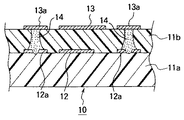
図1は本発明の多層配線基板の構成の1例を概略的に示す図であり、導体からなる配線層が、絶縁層を介して積層されたものである。 FIG. 1 is a diagram schematically showing an example of the configuration of a multilayer wiring board according to the present invention, in which a wiring layer made of a conductor is laminated via an insulating layer.
この多層配線基板10は、第1の絶縁層11aの上に第1の配線層12が形成されており、第1の配線層12はその回路パターンの一部として第1のビアランド12aを有している。第1の配線層12の上側から第1の絶縁層11a上にかけて第2の絶縁層11bが形成されており、この第2の絶縁層11b上には第2の配線層13が形成されている。
In this
この第2の配線層は、第1の配線層のビアランド12aと対向する位置に第2のビアランド13aを有している。
The second wiring layer has a second via
そして、第2の絶縁層11bを介して対向配置された第1のビアランドと第2のビアランドは、導電性ピラー14により接続されている。つまり、この多層配線基板10は、導電性ピラー14によって異なる配線層の層間接続を行っている。
Then, the first via land and the second via land arranged to face each other via the second insulating
本発明の多層配線基板10の特徴の1つとして、第1のビアランド12aは、導電性ピラー14の軸方向にかかる応力を分散する手段を有しており、この場合第1のビアランド12aには貫通孔12bが形成されている。
As one of the features of the
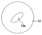
図2は第1のビアランドの形状の1例を概略的に示す図であり、第1の絶縁層11aにパターニングしたときの状態を示している。この第1のビアランド12aはほぼ円形の貫通孔12bを1個有しているが、貫通孔12bの形状および数はこれに限ることはない。貫通孔12bの形状としては、円形以外に例えば楕円形、星形、瓢箪型などでもよい。いずれにせよ、貫通孔12bの形状は、応力が特定の部分に集中しないように角ばった部分がない形状であることが好適である。
FIG. 2 is a diagram schematically showing an example of the shape of the first via land, and shows a state in which the first via land is patterned on the first insulating
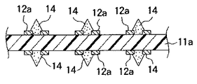
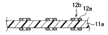
また、第1のビアランド12aには複数の貫通孔12bを備えるようにしてもよい。図3Aは第1のビアランドの形状の別の例を概略的に示す図である。
The first via
図4は図1に示した本発明の多層配線基板の層間接続部を拡大して示す図である。第1のビアランド12aと第2のビアランド13bとが導電性ピラー14によりビア接続されている。導電性ピラー14は、第1のビアランド12aに対応する領域で、第1の絶縁層11aに貫入した貫入部14bを有している。このような貫入部14bは、例えば第1のビアランドと第2のビアランドとの間に導電性ピラーを挟み込んだ状態で、第1の絶縁層と第2の配線層とを導電性ピラーの軸方向に加圧することにより形成される。本発明の多層配線基板はこのような構成を採用することにより、多層配線基板の層間接続方向、すなわち導電性ピラー14の軸方向に圧力負荷がかかった場合でも、第1のビアランド12aに形成した応力分散手段である貫通孔14bから導電性ピラーの一部が第1の絶縁層側に塑性変形しながら貫入することにより、第1のビアランド12aの破損を防ぐことができる。したがって多層配線基板の層間接続の信頼性が向上する。また、第1のビアランド12aが備える応力分散手段の形成を第1の配線層12のパターニングと同時に行えば、工程数を増やす必要もない。なお、導電性ピラーの剛性は第1の絶縁層よりも大きいが、貫入時にある程度変形する程度に設定することが好適である。
4 is an enlarged view showing an interlayer connection portion of the multilayer wiring board of the present invention shown in FIG. The first via
図5は、本発明の多層配線基板の構成の別の1例を概略的に示す断面図である。この多層配線基板20は、導体からなる4層の配線層を有している。各配線層はその回路パターンの一部として設けられたビアランドを有しており、絶縁層11bを介して対向した1対のビアランド間を導電性ピラー14により接続することにより配線層の層間接続を行っている。
FIG. 5 is a sectional view schematically showing another example of the configuration of the multilayer wiring board of the present invention. The
第1の絶縁層11aの両面には第1のビアランド12aを有する第1の配線層12が形成されている。この第1のビアランド12aには、応力分散手段として例えば図3に例示したような貫通孔12bが形成されている。第1の配線層12上には、第2の絶縁層11bが形成されており、第2の絶縁層11b上には第2のビアランド13aを有する第2の配線層13が形成されている。第1のビアランド12aと第2のビアランド13aとは、第2の絶縁層11b絶縁層を介して対向して形成されており、導電性ピラー14により層間接続されている。
A
なお、ここでは第1の絶縁層11aの両側に形成される配線層をどちらも第1の配線層12として説明している。いずれにせよ、当然ながら、第1の絶縁層11aの両側の形成される第1の配線層12の回路パターンは異なっていてもよい。同様に、外層に形成される第2の配線層13についてもその回路パターンは異なっていてもよい。すなわち、各配線層はその層間接続部にビアランドを有しているが、その回路パターンは必要に応じて形成される。このことは特に述べない場合にも同様である。
Here, the wiring layers formed on both sides of the first insulating
次に図5に例示した本発明の多層配線基板20の製造方法の1例を説明する。
Next, an example of a method for manufacturing the
図6A、図6B、図6Cは図5に示した本発明の多層配線基板の製造工程を説明するための図である。 6A, 6B, and 6C are views for explaining a manufacturing process of the multilayer wiring board of the present invention shown in FIG.
まず、絶縁層の両面に導体層を張り合わせたコア基材として、両面銅張積層板を用意する。ここでは第1の絶縁層11aである厚さ1.2mmの紙−フェノール樹脂系の絶縁基板の両面に、第1の配線層12にパターニングされる厚さ35μmの電解銅箔を張り合わせた両面銅張積層板(商品名、紙フェノール樹脂銅張積層板 R−8705E、松下電工製)を用意した。
First, a double-sided copper-clad laminate is prepared as a core base material in which a conductor layer is bonded to both sides of an insulating layer. Here, double-sided copper in which an electrolytic copper foil having a thickness of 35 μm to be patterned on the
次いで、このコア基材に張り付けられた第1の配線層12である銅箔を例えばフォトエッチングプロセスなどにより所定の配線回路にパターニングする。ここでは、銅箔上にスクリーン印刷で所定パターンのレジストを形成し、このレジストをマスクとして、塩化第2鉄溶液をエッチング液として、銅箔を選択的にエッチング除去した後、レジストを除去して、所定の回路パターンを有する第1の配線層12に形成した(図6A)。このとき、第1の配線層12の回路パターンの一部として第1のビアランド12aも形成した。第1のビアランド12aは直径約0.7mmの略円形に形成され、かつその中央部に直径約0.2mmの孔12bを形成した。
Next, the copper foil as the
なお、ここでは第1の絶縁層11aの両側に形成される配線回路をどちらも第1の配線回路として説明しているが、第1の絶縁層の両側で第1の配線層の回路パターンは異なるパターンに形成した。
Here, both the wiring circuits formed on both sides of the first insulating
次に、第1の配線回路12の第1のビアランド12a上に略円錐形状を有する導電性ピラー14を形成した。この導電性ピラー14は、第1のビアランド12aに対応する位置にピットを形成したメタルマスクを配置して、導電性樹脂をスクリーン印刷することにより形成した。メタルマスクは直径約0.3mmの孔を穿設した、厚さ約300μmのステンレス鋼製のものを用いた。導電性樹脂としては、この例では、銀粉末をフィラーとしたフェノール樹脂系の導電性ペーストを用いたが、導体からなるフィラー、バインダー樹脂とも必要に応じて選択して用いればよい。印刷した導電性ペーストを乾燥処理した後、同一マスクを用い同一位置に印刷、乾燥する処理を3回繰り返した。さらに加熱して、第1のビアランド12a上に略円錐形状を有する高さ約0.3mmの導電性ピラー14を形成した(図6B)。導電性ピラー14の形状は、例えば、用いるマスクのピット径、厚さ、または印刷する導電性樹脂の粘性などの諸物性、さらに印刷回数などを調節することにより所望の形状に形成することができる。
Next, the
導電性ピラー14を形成した後、第2の絶縁層11bと、第2の配線層13をコア材の両側に積層する。ここでは、第2の絶縁層11bとしては例えば厚さ約70μmのエポキシ系樹脂シート(Bステージ)を用い、第2の配線層13(未パターニング)としては、厚さ約35μmの電解銅箔を用いた。
After forming the
第2の絶縁層11bと第2の配線層13とを、コア基材の両側に、第2の配線層13が第2の絶縁層11bを介して第1の配線層12と対向するように配置して(図6C)、第2の配線層13の外側から、プレス板で挟み込んで加熱しながら加圧する。加熱と加圧により、第2の絶縁層11bは硬化してCステージになる。このとき、略円錐形状の導電性ピラー14は、セミキュア状態の第2の絶縁層11bを貫き、対向する第2のビアランド13aと接続する。第2の絶縁層11bの硬化が始まるのは、コア基材と第2の配線層13とが第2の絶縁層11bの両側に接した後だから、第1の配線層12上に形成した導電性ピラー14は、比較的容易に第2の絶縁層11bを貫くことができる。
The second
ここで、プレスの際に用いる当て板としては、例えばステンレス板、真鍮板などの寸法変化や変形の少ない金属板や、ポリイミド樹脂板(シート)、ポリテトラフロロエチレン樹脂板(樹脂シート)な寸法変化や変形の少ない耐熱性樹脂板などを使用することが好適である。 Here, as a backing plate used at the time of pressing, for example, a metal plate such as a stainless steel plate or a brass plate or a metal plate with little deformation and deformation, a polyimide resin plate (sheet), a polytetrafluoroethylene resin plate (resin sheet) It is preferable to use a heat-resistant resin plate with little change or deformation.
また、絶縁層を加熱して柔らかくなった状態でプレスを行うと、導電性ピラー先端が絶縁層を貫通し易くなる。 In addition, when pressing is performed in a state where the insulating layer is heated and softened, the conductive pillar tip easily penetrates the insulating layer.
次いで、第2の配線層13をパターニングして所定の回路に形成する。ここでは、第2の配線層13である銅箔上にスクリーン印刷で所定パターンのレジストを形成し、このレジストをマスクとして、塩化第2鉄溶液をエッチング液として、銅箔を選択的にエッチング除去した後、レジストを除去して第2のビアランドを有する所定の回路パターンに形成した。このとき、配線回路パターンの部として第2のビアランド13aも同時に形成した。
以上のような工程により、各配線層が導電性ピラーによる1000箇所のビア接続を有する4層の多層配線基板が形成された(図5参照)。
Next, the
Through the steps as described above, a four-layer multilayer wiring board in which each wiring layer has 1000 via connections with conductive pillars was formed (see FIG. 5).
このように製造した多層配線基板の配線回路の接続抵抗は約2.1Ωであった。この接続抵抗は、導電性ピラー1000個を銅箔からなる配線を介して直列に接続したときの抵抗に相当し、銅箔のパターン抵抗を考慮すると、導電性ピラー1本あたりの接続抵抗値の平均は約1mΩであった。また導電性ピラーの接続抵抗および銅箔のパターン抵抗ともバラツキが少ないものであった。 The connection resistance of the wiring circuit of the multilayer wiring board manufactured in this way was about 2.1Ω. This connection resistance corresponds to the resistance when 1000 conductive pillars are connected in series via a wiring made of copper foil, and considering the pattern resistance of the copper foil, the connection resistance value per conductive pillar is The average was about 1 mΩ. Further, the connection resistance of the conductive pillar and the pattern resistance of the copper foil were less varied.
また、この多層配線基板を導電性ピラーの軸方向と平行な平面で切断して、層間接続部の状態を観察したところ、図4に模式的に示したように、導電性ピラー14と第1のビアランドおよび第2ビアランドは密に接続し、接合状態も良好であった。第2のビアランド12aは第1の絶縁層側にわずかに若干窪んでいるが、亀裂の発生は認められなかった。また、導電性ピラー14の一部は、第2のビアランド12aに形成した孔12bを通じて第1の絶縁層11a側に貫入した部分を有していた。
Further, when this multilayer wiring board was cut along a plane parallel to the axial direction of the conductive pillar and the state of the interlayer connection portion was observed, as shown schematically in FIG. The via land and the second via land were closely connected, and the bonding state was also good. The second via
なお、比較のため、第1のビアランド12aに応力分散手段を形成しないこと以外は図5と同じ構成を有する多層配線を同一条件で製作した。この導電性ピラーによる1000箇所のビア接続を有する四層の多層配線基板の配線パターンの接続抵抗は5.1Ωで、図5に例示した本発明の多層配線基板の接続抵抗よりも約3Ωも大きかった。また、第1のビアランドに応力分散手段を備えない多層配線基板を切断してビア接続の状態を観察したところ、第1のビアランド12a部分が大きく第1の絶縁層11a側に窪んでいた。第1のビアランド12aには亀裂が発生していた。
For comparison, a multilayer wiring having the same configuration as that of FIG. 5 was manufactured under the same conditions except that the stress distribution means was not formed on the first via
このように本発明の多層配線基板は、応力分散手段を備えたビアランドを備えることにより、導電性ピラーの軸方向にかかるビアランドへの応力(圧力)を分散することができる。また、ビアランドの接線方向にかかる応力(接線応力)は、主として導電性ピラーの塑性変形により緩和される。したがって、ビアランドを含む配線回路が破損しにくく、信頼性の高い層間接続を確立することができる。また、スルーホールによる層間接続を必要最小限に抑制することができるため、高密度実装に対応することができる。
また本発明の多層配線基板の製造方法によれば、導電性ピラーを用いた多層配線基板の製造方法の高い生産性を保ちながら、接続不良の発生を抑制し、さらに生産性を向上することができる。
As described above, the multilayer wiring board of the present invention can disperse the stress (pressure) applied to the via land in the axial direction of the conductive pillar by including the via land including the stress dispersing means. Further, the stress (tangential stress) applied in the tangential direction of the via land is relieved mainly by plastic deformation of the conductive pillar. Therefore, the wiring circuit including the via land is hardly damaged, and a highly reliable interlayer connection can be established. In addition, since interlayer connection by through holes can be suppressed to a necessary minimum, high-density mounting can be supported.
In addition, according to the method for manufacturing a multilayer wiring board of the present invention, while maintaining high productivity of the method for manufacturing a multilayer wiring board using conductive pillars, it is possible to suppress the occurrence of poor connection and further improve productivity. it can.
図7A、図7B、図7C、図7Dは本発明の多層配線基板の製造方法の別の例について説明するための図である。 FIG. 7A, FIG. 7B, FIG. 7C, and FIG. 7D are diagrams for explaining another example of the method for manufacturing a multilayer wiring board according to the present invention.
まず、絶縁層の両面に導体層を張り合わせたコア基材として、両面銅張積層板を用意する。ここでは厚さ1.2mmの紙−フェノール樹脂系の絶縁基板の両面に、第1の配線層12にパターニングされる厚さ35μmの電解銅箔を張り合わせた両面銅張積層板(商品名、紙フェノール樹脂銅張積層板 R−8705E、松下電工製)を用意した。
次いで、このコア基材に張り付けられた銅箔を例えばフォトエッチングプロセスなどにより所定の配線回路にパターニングする。ここでは、銅箔上にスクリーン印刷で所定パターンのレジストを形成し、このレジストをマスクとして、塩化第2鉄溶液をエッチング液として、銅箔を選択的にエッチング除去した後、レジストを除去して、所定の回路パターンを有する第1の配線層12に形成した(図7A)。このとき、第1の配線層12の配線回路パターンの一部として第1のビアランドも形成した。第1のビアランド12aは直径約0.7mmの略円形に形成され、かつその中央部に直径約0.2mmの孔12bを形成した。
なお、ここでは第1の絶縁層11aの両側に形成される配線回路をどちらも第1の配線回路として説明しているが、第1の絶縁層の両側で第1の配線層の回路パターンは異なるパターンに形成した。
First, a double-sided copper-clad laminate is prepared as a core base material in which a conductor layer is bonded to both sides of an insulating layer. Here, a double-sided copper-clad laminate (trade name, paper) in which a 35-μm-thick electrolytic copper foil patterned on the
Next, the copper foil attached to the core substrate is patterned into a predetermined wiring circuit by, for example, a photoetching process. Here, a resist having a predetermined pattern is formed on the copper foil by screen printing, and the copper foil is selectively removed by etching using the ferric chloride solution as an etching solution, and then the resist is removed. The
Here, both the wiring circuits formed on both sides of the first insulating
一方、第2の配線層13として、厚さ約35μmの電解銅箔を用意し、この電解銅箔上に略円錐形状を有する導電性ピラー14を形成した。
On the other hand, an electrolytic copper foil having a thickness of about 35 μm was prepared as the
この導電性ピラー14は、第2の配線層13を第1の配線層12と重ねたとき第1の配線層12に形成した第1のビアランド12aと対応する位置に形成した。
The
導電性ピラー14の形成は、ピットを形成したメタルマスクを配置して、導電性樹脂をスクリーン印刷することにより形成した。メタルマスクは直径約0.3mmの孔を穿設した、厚さ約300μmのステンレス鋼製のものを用いた。導電性樹脂としては、この例では、銀粉末をフィラーとしたフェノール樹脂系の導電性ペーストを用いた。印刷した導電性ペーストを乾燥処理した後、同一マスクを用い同一位置に印刷、乾燥する処理を3回繰り返した。さらに加熱して、第1のビアランド12a上に略円錐形状を有する高さ約0.3mmの導電性ピラー14を形成した(図7B)。
The
第1の絶縁層11aの両面に第1の配線層12を形成したコア材と、導電性ピラー14を形成した第2の配線層(未パターニング)をそれぞれ用意した後、図7Cに示すように、コア材の両側に第2の絶縁層11bを介して第2の配線層を配置する。このとき、第1のビアランド12aと、導電性ピラー14とが対向するように位置あわせして配置する。
As shown in FIG. 7C, after preparing a core material in which the
第2の絶縁層11bとしては、ガラスクロスにエポキシ系樹脂を含浸させた厚さ約100μmのBステージのプリプレグを用いた。
As the second insulating
そして、第2の配線層13の外側から、プレス板で挟み込んで加熱しながら全体を加圧する。加熱と加圧により第2の絶縁層11bはCステージに硬化する。
Then, the whole is pressed from the outside of the
このとき、略円錐形状の導電性ピラー14は、セミキュア状態の第2の絶縁層11bを貫き、対向する第1のビアランド12aと接続する。第2の絶縁層11bの硬化が始まるのは、コア基材と第2の配線層13とが第2の絶縁層11bの両側に接した後だから、第2の配線層13上に形成した導電性ピラー14は、比較的容易に第2の絶縁層11bを貫くことができる。
At this time, the substantially conical
導電性ピラー14の先端部は第1のビアランド12aに形成した応力分散手段である貫通孔12bに挿入され、塑性変形しながら第1のビアランド12aと密着する。ここでは導電性ピラー14は、塑性変形しながら第1の絶縁層11aに貫入するものの、第1の絶縁層11aを容易に刺し貫けるほど堅くないので、第1のビアランドを破損することなく密着することができる。
The leading end portion of the
次いで、第2の配線層をパターニングして所定の回路に形成する。ここでは、第2の配線層13である銅箔上にスクリーン印刷で所定パターンのレジストを形成し、このレジストをマスクとして、塩化第2鉄溶液をエッチング液として、銅箔を選択的にエッチング除去した後、レジストを除去して第2のビアランドを有する所定の回路パターンに形成した。
以上のような工程により、各配線層が導電性ピラーによる1000箇所のビア接続を有する4層の多層配線基板が形成された(図7D)。
Next, the second wiring layer is patterned to form a predetermined circuit. Here, a resist of a predetermined pattern is formed on the copper foil as the
Through the steps as described above, a four-layer multilayer wiring board in which each wiring layer has 1000 via connections with conductive pillars was formed (FIG. 7D).
このように製造した多層配線基板の配線回路の接続抵抗は約2.1Ωであった。この接続抵抗は、導電性ピラー1000個を銅箔からなる配線を介して直列に接続したときの抵抗に相当し、銅箔のパターン抵抗を考慮すると、導電性ピラー1本あたりの接続抵抗値の平均は約1mΩであった。また導電性ピラーの接続抵抗および銅箔のパターン抵抗ともバラツキが少ないものであった。 The connection resistance of the wiring circuit of the multilayer wiring board manufactured in this way was about 2.1Ω. This connection resistance corresponds to the resistance when 1000 conductive pillars are connected in series via a wiring made of copper foil, and considering the pattern resistance of the copper foil, the connection resistance value per conductive pillar is The average was about 1 mΩ. Further, the connection resistance of the conductive pillar and the pattern resistance of the copper foil were less varied.
図8は、図7Dの多層配線基板を導電性ピラーの軸方向と平行な平面で切断して、層間接続部の状態を観察した様子を示す図である。導電性ピラー14の一部は、第1のビアランド12aに形成した孔12bを通じて第1の絶縁層11a側に貫入した部分14cを有していたが、導電性ピラー14と第1のビアランドおよび第2ビアランドは密に接続し、接合状態も良好であった。
FIG. 8 is a view showing a state in which the state of the interlayer connection portion is observed by cutting the multilayer wiring board of FIG. 7D along a plane parallel to the axial direction of the conductive pillar. A part of the
第2のビアランド12aは第1の絶縁層側にわずかに若干窪んでいるが、亀裂の発生は認められなかった。これは、導電性バンプ14が第1のビアランド12aに設けられた孔12bを通じて第1の絶縁層11aに貫入するとともに、第1のビアランド12aに沿って塑性変形したためである。
The second via
なお、比較のため、第1のビアランド12aに応力分散手段を形成しないこと以外は図7Dと同じ構成を有する多層配線を同一条件で製作した。この導電性ピラーによる1000箇所のビア接続を有する四層の多層配線基板の配線パターンの接続抵抗は5.1Ωで、図7Dに例示した本発明の多層配線基板の接続抵抗よりも約3Ωも大きかった。また、第1のビアランドに応力分散手段を備えない多層配線基板を切断してビア接続の状態を観察したところ、第1のビアランド12a部分が大きく第1の絶縁層11a側に窪んでいた。第1のビアランド12aには亀裂が発生していた(図27参照)。
For comparison, a multilayer wiring having the same configuration as that of FIG. 7D was manufactured under the same conditions except that the stress distribution means was not formed on the first via
このように本発明の多層配線基板は、応力分散手段を備えたビアランドを備えることにより、導電性ピラーの軸方向にかかる応力を分散することができる。したがって、ビアランドを含む配線回路が破損しにくく、信頼性の高い層間接続を確立することができる。また、スルーホールによる層間接続を必要最小限に抑制することができるため、高密度実装に対応することができる。 Thus, the multilayer wiring board of the present invention can disperse the stress applied in the axial direction of the conductive pillar by including the via land including the stress dispersing means. Therefore, the wiring circuit including the via land is hardly damaged, and a highly reliable interlayer connection can be established. In addition, since interlayer connection by through holes can be suppressed to a necessary minimum, high-density mounting can be supported.
また本発明の多層配線基板の製造方法によれば、導電性ピラーを用いた多層配線基板の製造方法の高い生産性を保ちながら、接続不良の発生を抑制し、さらに生産性を向上することができる。 In addition, according to the method for manufacturing a multilayer wiring board of the present invention, while maintaining high productivity of the method for manufacturing a multilayer wiring board using conductive pillars, it is possible to suppress the occurrence of poor connection and further improve productivity. it can.
本発明は上記実施例に限定されるものでなく、発明の趣旨を逸脱しない範囲でいろいろの変形を採ることができる。たとえば、配線層は、導電性組成物で形成してもよいし、また導電性ピラーは金属製でもよい。さらに絶縁層もエポキシ系樹脂に限らず、熱硬化性樹脂、熱可塑性樹脂などを必要に応じて選択して用いることができる。 The present invention is not limited to the above embodiments, and various modifications can be made without departing from the spirit of the invention. For example, the wiring layer may be formed of a conductive composition, and the conductive pillar may be made of metal. Furthermore, the insulating layer is not limited to an epoxy resin, and a thermosetting resin, a thermoplastic resin, or the like can be selected and used as necessary.
図9Aは、本発明の多層配線基板の層間接続部の断面構造を概略的に示す図である。図9Bは図9Aに示した層間接続部の構造を導電性ピラーの軸方向から透視して概略的に示す図であり、図9Cは図9Aに示した層間接続部の構造を概略的に示す斜視図である。 FIG. 9A is a diagram schematically showing a cross-sectional structure of an interlayer connection portion of the multilayer wiring board of the present invention. 9B is a diagram schematically showing the structure of the interlayer connection portion shown in FIG. 9A as seen through from the axial direction of the conductive pillar, and FIG. 9C is a diagram schematically showing the structure of the interlayer connection portion shown in FIG. 9A. It is a perspective view.
この多層配線基板は、絶縁性膜21と、この絶縁性膜21の第1の面に形成された第1のビアランド22と、絶縁性膜21の第2の面に形成され、第1のビアランド22と対向する領域に形成された第2のビアランド23とを備えている。
This multilayer wiring board is formed on the insulating
ここで第1のビアランド22は第1の配線層の回路パターン22bの一部として形成されており、第2のビアランド23は図示しない第2の配線層の回路パターン23bの一部として形成されている。
Here, the first via
そして、第1の配線層と第2の配線層との層間接続は、第1のビアランド22と第2のビアランド23とを接続するように絶縁性膜21を貫通して形成された導体からなる導電性ピラー24とにより確立されている。そして、この導電性ピラー24の外側面と第1のビアランド22および第2のビアランド23の表面とが接する部分の形状は、導電性ピラー24と第1のビアランド22または第2のビアランド23との接続部の固体−固体界面に応力集中が生じないように形成されている。
The interlayer connection between the first wiring layer and the second wiring layer is made of a conductor formed so as to penetrate the insulating
導電性ピラー24と第1のビアランド22、第2のビアランド23との接続部の界面に応力集中が生じないようにするには、例えば、導電性ピラー24の外側面と第1のビアランド22および第2のビアランド23の絶縁性膜21側の表面とのなす接触角をできるだけ応力集中係数が小さくなるように設定すればよい。
In order to prevent stress concentration from occurring at the interface between the connecting portions of the
図10A、図10B、図10Cは、本発明の多層配線基板の有する導電性ピラー24と第1のビアランド22(または第2のビアランド23)との接続部の形状の例を模式的に示す図である。図11A、図11Bは比較のために示した導電性ピラー24と第1のビアランド22(または第2のビアランド23)との接続部の形状の、望ましくない形状の例である。
10A, 10B, and 10C are diagrams schematically showing an example of the shape of the connection portion between the
本発明者は、導電性ピラーを採用したビア接続部に生じる応力を、各材料の物性定数を用いてシミュレーションで解析した結果、導電性ピラー24と配線層またはビアランドとを引きはがすように働く応力は、配線層(またはビアランド)と導電性ピラー24が接続する部分で、ビアランドの表面と、導電性ピラーの外周面の形成する角度に依存していることがわかった。したがって、本発明では、概単双曲面形状を有する導電性ピラーの外周面とビアランド表面との接触角θを、応力集中係数が小さくなるように制御して形成している。
As a result of analyzing the stress generated in the via connection portion employing the conductive pillar by simulation using the physical constants of each material, the present inventor has found that the stress acts to peel off the
例えば、導電性ピラー24の外側面とビアランド22の表面とが、滑らかに連続するように接触角θを小さく設定すれば、接合強度、耐剥離強度を向上することができる。例えば図10Bに示した形状を有するビア接続は、図10Cに示した形状を有するビア接続よりも剥離に対する強度は大きい。同様に図10Aに示した形状を有するビア接続は、図10Bに示した形状を有するビア接続よりも剥離に対する強度は大きい。いずれにせよ、図10Cに示した形状を有するビア接続でも、図11A、図11Bに示した形状を有するビア接続よりも耐剥離強度はずっと大きい。
For example, if the contact angle θ is set small so that the outer surface of the
すなわち、導電性ピラーの外周面と、ビアランドの表面が滑らかに連続して接続している場合には、剥離に対抗する強度が大きいが、導電性ピラーの外周面とビアランドとの接合部にノッチがあるとこの部分に応力が集中して耐剥離強度が低下し、ノッチが鋭いほど耐剥離強度の低下は大きくなる。 That is, when the outer peripheral surface of the conductive pillar and the surface of the via land are connected smoothly and continuously, the strength against the peeling is high, but the notch is formed at the joint between the outer peripheral surface of the conductive pillar and the via land. If there is, stress concentrates on this part and the peel strength decreases, and the sharper the notch, the greater the decrease in peel strength.
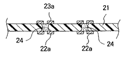
また、導電性ピラーの外周面とビアランドの表面とが全体として滑らかに接続していれば、ミクロスコピックなノッチがあっても剥離強度を維持することができることもわかった。図12A、図12Bは、導電性ピラーと第1のビアランドまたは第2のビアランドとの接続部の形状の別の例を模式的に示す図である。導電性ピラーの外周面とビアランド表面の接続部は閉曲線、例えば円を描くが、この閉曲線上のすべての部分が滑らかに接続している場合に耐剥離強度は最大になる。いずれにせよ、この閉曲線の少なくとも一部が滑らかに接続しているならば、閉曲線のすべての部分に応力集中係数の大きい形状のノッチを有して接続している場合と比較して、耐剥離強度を大きくすることができる。例えば、図12A、図12Bに示した形状は、ミクロスコピックにはノッチを有しているが(接触角ψ)、導電性ピラー24の外側面とビアランドの表面とは全体として滑らかに連続して接続しており(接触角θ)、半田リフローなどの実装プロセスで熱的負荷がかかる場合であっても、配線層間のビア接続を安定して維持することができる。
It was also found that if the outer peripheral surface of the conductive pillar and the surface of the via land are smoothly connected as a whole, the peel strength can be maintained even if there is a microscopic notch. 12A and 12B are diagrams schematically illustrating another example of the shape of the connection portion between the conductive pillar and the first via land or the second via land. The connection portion between the outer peripheral surface of the conductive pillar and the via land surface draws a closed curve, for example, a circle. When all the portions on the closed curve are smoothly connected, the peel resistance is maximized. In any case, if at least a part of this closed curve is connected smoothly, it is more resistant to delamination compared to the case where all parts of the closed curve are connected with a notch with a large stress concentration factor. The strength can be increased. For example, the shape shown in FIGS. 12A and 12B has a notch in the microscopic (contact angle ψ), but the outer surface of the
図13Aは本発明の多層配線基板の構造の1例を模式的に示す図であり、図13Bは図13Aの多層配線基板に熱負荷がかかったときの状態を模式的に示す図である。この多層配線基板は、導電性ピラー24を採用したビア接続を3000箇所有している。
図13Aの多層配線基板の層間接続部は、図9Aに示した本発明の多層配線基板と同様の構造を有している。絶縁層21を貫通して形成された導電性ピラー24は、絶縁層21により隔てられた第1の配線層の第1のビアランド23と第2の配線層の第2のビアランド24とを接続している。そして、導電性ピラー24と第1のビアランド22のおよび第2のビアランド23との接合部はどちらも3重点25にかかる応力を緩和するような形状を有している。この例では導電性ピラー24の外周面と第1のビアランド22の表面とのなす角、および導電性ピラー24の外周面と第2のビアランド23の表面とのなす角は、どちらも鋭角に形成されている。
FIG. 13A is a diagram schematically illustrating an example of the structure of the multilayer wiring board of the present invention, and FIG. 13B is a diagram schematically illustrating a state when a thermal load is applied to the multilayer wiring substrate of FIG. 13A. This multilayer wiring board has 3000 via connections that employ
The interlayer connection portion of the multilayer wiring board of FIG. 13A has the same structure as the multilayer wiring board of the present invention shown in FIG. 9A. The
このような多層配線基板に各種電子部品を実装する際、特に半田のリフローなどの際には、層間接続部に熱負荷がかかって熱膨張率の差に起因する応力が生じ、特に3重点25には応力が集中することになる。 When various electronic components are mounted on such a multilayer wiring board, particularly when solder is reflowed, a heat load is applied to the interlayer connection portion, resulting in a stress caused by a difference in thermal expansion coefficient. Stress will be concentrated on.
図13Aの多層配線基板は、絶縁層21としてFR−4規格の絶縁性樹脂基材を用い、配線層としては銅箔を用い、導電性ピラーとしては、銀の微粒子をフィラーとしてバインダー樹脂に分散させた導電性樹脂を用いている。
The multilayer wiring board of FIG. 13A uses an FR-4 standard insulating resin base material as the insulating
FR−4のガラス転移温度Tg(約125℃)より低い温度での、絶縁層21の法線方向の熱膨張率α1は5.1×10⁻⁵[°K-1]である。またTgより高い温度での、FR−4の厚さ方向の熱膨張率α2は2.6×10⁻⁴[°K-1]とα1よりずっと大きい。
The thermal expansion coefficient α1 in the normal direction of the insulating
一方、導電性ピラーの主要部を構成する銀の熱膨張係数は17.0×10⁻⁶[°K-1]である。したがって、図13Aの多層配線基板に熱負荷がかかったとき、絶縁層21のほうが導電性ピラー24よりも大きく膨張する。とくにガラス転移温度Tgより高い温度では、絶縁層21の熱膨張率は、銀の熱膨張係数と比較して15倍以上も大きい。半田として一般的なPb−Sn系の共晶半田合金の共晶温度は183℃であるから、半田をリフローする際には多層基板にも220〜240℃程度の熱負荷がかかることになる(図13B)。
On the other hand, the thermal expansion coefficient of silver constituting the main part of the conductive pillar is 17.0 × 10 −6 [° K −1 ]. Therefore, when a thermal load is applied to the multilayer wiring board of FIG. 13A, the insulating
したがって、導電性ピラー24の熱膨張率と絶縁層21との熱膨張率の差に起因して、導電性ピラー24の軸方向(絶縁層の法線方向と平行)に、大きな応力が発生する。この応力は、導電性ピラー24と第1のビアランド22および第2のビアランド23との接合部に対して張力として作用する。また、このような応力は、絶縁層21、導電性ピラー24およびビアランド22、23の3つの部分が接する3重点で最も大きくなる。
Therefore, a large stress is generated in the axial direction of the conductive pillar 24 (parallel to the normal direction of the insulating layer) due to the difference between the thermal expansion coefficient of the
図13Aに示した多層配線基板を240℃に20秒間加熱して、層間接続を調べたところ、すべての層間接続部が導通を確保しており、抵抗値も維持されていた。 The multilayer wiring board shown in FIG. 13A was heated to 240 ° C. for 20 seconds to examine the interlayer connection. As a result, all the interlayer connection portions were kept conductive and the resistance value was maintained.
なお、第1のビアランド22、第2のビアランド23として、例えば図2に例示したような導電性ピラーとビアランドとの間にかかる圧力をリリースする手段を設けてもよい。例えば第1のビアランド22または第2のビアランド23に貫通孔12bを形成すれば、導電性ピラーとビアランドとの間に圧力がかかる場合でも、張力がかかる場合でも、ビア接続の損傷を防ぎ、層間接続の機能を安定して維持することができる。
As the first via
図9から図13では1層の絶縁層の両面に形成された配線層の層間接続について示したが、上述のビア接続は3層以上の配線層を備えた多層配線基板にも全く同様に適用することができる。 9 to 13 show the interlayer connection of wiring layers formed on both surfaces of one insulating layer, but the above-described via connection is also applied to a multilayer wiring board having three or more wiring layers in the same manner. can do.
次に、導電性ピラーと第1のビアランドおよび第2のビアランドとの接合部にかかる応力を緩和するような形状を有する本発明の多層配線基板の製造方法について説明する。
図14A、図14B、図14C、図14D、図14E、図14F、図14Gは本発明の多層配線基板の製造方法の1例を説明するための図である。
Next, a method for manufacturing a multilayer wiring board of the present invention having a shape that relieves stress applied to the joint between the conductive pillar, the first via land, and the second via land will be described.
FIG. 14A, FIG. 14B, FIG. 14C, FIG. 14D, FIG. 14E, FIG. 14F, and FIG. 14G are views for explaining an example of the method for manufacturing a multilayer wiring board according to the present invention.
第1の配線層22となる厚さ約35μmの電解銅箔を用意し、この銅箔上の所定の位置に導電性ピラー24を形成した。この導電性ピラー24は、銀の微粒子(平均粒径約10μm)を導体フィラーとした導電性ペーストをスクリーン印刷して形成し、その底面の直径は約250μm、高さは約250μmの略円錐形状を有する(図14A)。
An electrolytic copper foil having a thickness of about 35 μm serving as the
導電性ピラー24を乾燥させた後に、絶縁層21としてガラスクロスにエポキシ系樹脂を含浸させた厚さ約115μmの熱硬化性のプリプレグ(商品名、ガラエポプリプレグHE、東芝ケミカル社製)を用意し、第1の配線層22の導電性ピラー24を形成した面上に積層配置した。このとき、Bステージの絶縁層21を約100℃(<Tg)に加温するとともに、フレキシブルな押圧体26で、導電性ピラー24が変形しないようにプレスすることにより、導電性ピラー24は絶縁層21を貫通した(図14B)。このとき絶縁層21完全に硬化しておらずセミキュア状態を保っている。これは、本発明の多層配線基板のプレハブ素材に相当する。ここでプレハブ素材とは多層配線基板を構成するprefabricatedされた素材という意味であり、例えば図14Bの状態あるいは図14Cの状態のものを指す。このような本発明の多層配線基板のプレハブ素材を用いることにより、本発明の多層配線基板を容易に構成することができる。例えば両面積層板の両面に図14Cのプレハブ素材を積層することにより、4層の配線層を有する本発明の多層配線基板を構成することができる。
After the
その後、絶縁層21から突出した導電性ピラー24の先端部を、導電性ピラー24の中心軸方向に加圧して変形させた。ここでは、導電性ピラー24上に厚さ1mm程度の硬質ステンレス鋼板を載置し、常温で平板プレスを行って、導電性ピラーの先端部がつぶれるように塑性変形させた(図14C)。このとき、絶縁層21の表面からは導電性ピラー24の潰れた頭部がわずかに盛り上がって露出していた。この状態でも、多層配線基板のプレハブ素材として用いることができる。
Thereafter, the tip of the
次いで、導電性ピラー24の先端部が露出した絶縁層21の表面に、第2の配線層となる厚さ約35μmの電解銅箔を配置した。この積層体を第1の配線層22および第2の配線層23の外側から加熱しながらプレスし、セミキュア状態の絶縁層21を加熱により完全に硬化させるとともに、導電性ピラー24と第2の配線層を圧着した(図14D)。ここまでの工程で、第1の配線層22と第2の配線層23とが導電性ピラー24により絶縁層21を介して層間接続された両面銅張板が得られる。導電性ピラー24はその形状を制御して形成し、まず絶縁層21から突出した頭部を潰され、つぎに第2の配線層23と圧着されることにより多段階に塑性変形する。そして、導電性ピラー24と配線層との接合部に応力が集中しないような形状を得ることができる。
Next, an electrolytic copper foil having a thickness of about 35 μm serving as a second wiring layer was disposed on the surface of the insulating
つぎに、第1の配線層22、第2の配線層23を、第1のビアランド22a、第2のビアランド22bを含む所定の配線回路にパターニングした(図14E)。この製造例では、一般的なエッチングレジストインク(PSR−4000H、太陽インキKK製)を、所定の配線回路パターンが得られるように、スクリーン印刷してマスクを形成し、塩化第2銅で銅箔をエッチングし、レジストマスク剥離した。図14Eに示した第1の配線層22と第2の配線層23とを有する2層配線基板をコア基材としてさらに多くの配線層を有する多層配線基板を製造する場合には、配線回路のパターニングと同時に、第1のビアランド22a、第2のビアランド23aに例えば図2に示したような応力解放手段を形成することが好適である(図14F)。応力解放手段を形成しておくことにより、外側の配線層との層間接続を形成する際のビアランド、配線回路の損傷が防止され、多層配線基板の信頼性を向上することができる。
Next, the
図14Eの状態で、常套的方法によりビア接続部の導通テストを行ったところ、全て(3000個)の導電性ピラー24を有する層間接続に異常は認められなかった。抵抗値にも異常は認められなかった。
In the state shown in FIG. 14E, when the continuity test of the via connection portion was performed by a conventional method, no abnormality was found in the interlayer connection having all (3000)
つぎに、図14Eに示した状態の多層配線基板をコア基材として、この両側にさらに第3の配線層27a、27bを有する4層の多層配線基板を製造した例について説明する。
Next, an example will be described in which a multilayer wiring board in the state shown in FIG. 14E is used as a core base material and a four-layer multilayer wiring board having
前述同様の方法で、図14Cに示したような、所定の位置に導電性ピラー24を形成した第3の配線層27a、27bと絶縁層21bを積層したプレハブ素材を用意する。ここでは、絶縁層21bは絶縁層21と同材質のプリプレグを用いたが、必要ならば、材質の異なる絶縁材料を用いることができる。
In the same manner as described above, a prefabricated material in which the
そして、図14Eに示した両面配線基板をコア基材として、この両側に第3の配線層27a、27bと絶縁層21bとを配置する。このとき、第1の配線層22および第2の配線層23と第3の配線層27a、27bとのビア接続部をそれぞれ対向するように配置する(図14G)。
Then, using the double-sided wiring board shown in FIG. 14E as a core base material, the
次いで、この積層体を第3の配線層27a、27bの外側から加熱しながらプレスして、セミキュア状態の絶縁層21bを加熱により完全に硬化させるとともに、導電性ピラー24と第3の配線層27a、27bを圧着した。
Next, this laminated body is pressed while being heated from the outside of the
そして第3の配線層27a、27bを所定の配線回路にパターニングすることにより、第1の配線層22および第2の配線層23と、第3の配線層27a、27bが導電性ピラー24により絶縁層21bを介して層間接続された4層の配線層を有する多層配線基板が得られる(図14H)。
Then, by patterning the
このような耐剥離強度の大きい接合形状を有する本発明の多層配線基板の製造方法についてさらに詳しく説明する。まず、第1の配線層22と導電性ピラー24との接合について説明し、つぎに第2の配線層と導電性ピラー24との接合形状について説明する。
The method for producing the multilayer wiring board of the present invention having such a bonded shape having a high peel strength will be described in more detail. First, the bonding between the
図14の例では第1の配線層22と導電性ピラー24との接合形状は、例えば銅箔などの第1の配線層22上に導電性ピラーを形成するときに実質的に決定される。例えば、メタルマスクなどのマスクを用いて、導電性樹脂、導電性ペーストなどをスクリーン印刷して導電性ピラーを形成する場合には、メタルマスクの形状、開口径、厚さを調節し、一方導電性樹脂層の粘性、チキソトロピー、表面張力、またはマスクの表面張力などの物性値を調節することにより導電性ピラーを所望の形状に形成することができる。
ここで、導電性ピラーの形成方法について説明する。ここでは、多層配線基板を例にとって導電性ピラーを形成する方法を説明する。
In the example of FIG. 14, the bonding shape between the
Here, a method for forming the conductive pillar will be described. Here, a method of forming conductive pillars will be described taking a multilayer wiring board as an example.
図15A、図15B、図15C、図15D、図15Eは導電性ピラー24の形成工程の1例を説明するための図である。
FIG. 15A, FIG. 15B, FIG. 15C, FIG. 15D, and FIG. 15E are diagrams for explaining an example of the formation process of the
第1の配線層22上に略円柱形状を有する貫通孔(ピット)31aを形成したメタルマスク31を配置した。ここでメタルマスクは厚さ300μmのステンレススチール製で、貫通孔31aの直径は3.00μmに設定した。
A
そして、スクリーン32を介して、導電性樹脂33をスキージ34によりメタルマスク31の孔31aに充填する(図15A、図15B)。図15Cはスクリーン印刷の様子の1例を説明するための図である。
Then, the
ここでは導電性樹脂33としては、銀の微粒子をエポキシ系のバインダー樹脂に混練したものに、さらに溶剤を混合して用いた。通常、導電性樹脂33は数百ポアズ程度に粘性を調節して使用するのが一般的であるが、本発明では導電性ピラーの形状を制御するためにこれよりもずっと粘性を大きく調節して用いた。また必要であれば、例えば超音波振動などにより導電性樹脂33のチキソトロピーを調節して(ただし導電性樹脂33がチキソ性を有する場合)用いるようにしてもよい。
Here, as the
このように、粘性を調節した導電性樹脂33をメタルマスク31の孔31aに充填したなら、メタルマスク31と第1の配線層22とを第1の配線層22の法線方向に離間させる(図15D)。このとき導電性樹脂33は、第1の配線層22とメタルマスク31との間に張られながら変形し、第1の配線層22上に略円錐形状を有する導電性ピラー24が形成された(15E)。形成された略円錐形状を有する導電性ピラー24の底面の直径rは約300μm、高さhは約250μmであった。また、導電性樹脂33の一部はメタルマスク31の孔31aに付着していた。このような方法により、導電性ピラー24と第1の配線層22の表面との接触角θは小さく、ノッチ効果を緩和するような接合形状を得ることができる。さらにアスペクト比(高さ(h)/底面の直径(r))の高い導電性ピラー24を形成したい場合には、例えば、貫通孔31aの形状と導電性樹脂33の物性を調節するようにしてもよいし、またメタルマスク31を同じ位置に配置し、スクリーン印刷を繰り返すようにしてもよい。
In this way, when the
また、導電性ピラー24の形成はスクリーン印刷に限らず、導電性ペーストをマスクの孔に押し出すスタンプ法などにより形成するようにしてもよい。このような方法によっても、スクリーン印刷と同様に導電性ペースト、導電性樹脂などからアスペクト比の高い導電性ピラー24を形成することができる。またメッキ法などにより金属からなる導電性ピラーを形成するようにしてもよい。いずれの場合でも、導電性ピラー24の高さ、径は、後述するように、形成するビア接続部の構成に応じて設定すればよい。
The
なお上述の導電性ピラーの形成方法は多層配線基板の層間接続を例にとって説明したが、例えば半導体素子などの電子部品の電極上にも全く同様の方法で形成することができる。
つぎに、このように形成した導電性ピラー24と第2の配線層23との接合形状を制御する方法について説明する。
Although the above-described method for forming the conductive pillar has been described by taking the interlayer connection of the multilayer wiring board as an example, it can be formed on the electrode of an electronic component such as a semiconductor element by the same method.
Next, a method for controlling the joint shape between the
図16は導電性ピラー24と絶縁層21との関係を概略的に示す図であり、実施例7の図14Bの状態に相当する。本発明者は、導電性ピラー24と第2の配線層23との接合形状は、導電性ピラー24の絶縁層21に埋まった部分と、絶縁層21の表面から突出した部分との質量の比、および、導電性ピラー24の塑性変形能などの物性値と関係することを実験により見い出だした。
FIG. 16 is a diagram schematically showing the relationship between the
例えば、配線層として電解銅箔を用い、導電性ピラー24の主要部を構成する導体フィラーとして銀の微粒子を用いた場合には、絶縁層21の厚さdに対して、導電性ピラー24の高さhを1〜5倍大きく、より好ましくは1.6〜4倍大きく設定することにより、導電性ピラー24と第2の配線層23の表面との接触角θの小さなノッチ効果を緩和するような接合形状を得ることができることがわかった。
For example, when electrolytic copper foil is used as the wiring layer and silver fine particles are used as the conductor filler constituting the main part of the
ここで、導電性ピラー24の高さhを絶縁層21の厚さdよりも大きく設定するのは、次のような理由に基づくものである。例えば絶縁層21が熱硬化性樹脂の場合は、そのBステージからCステージへ硬化する際に厚さdは0〜30%程度収縮し、また、熱可塑性樹脂の場合は、軟化状態から固化することによってその厚さdは0〜15%程度収縮する。したがって、導電性ピラー24の高さhが、少なくとも絶縁層21の厚さの1.2倍を超える高さであれば、少なくとも先端部が絶縁層21の表面から突出することになる。この突出する部分は、第2の配線層23と圧着される際に塑性変形して接合形状を形成する部分である。そして導電性ピラー24の高さhが、絶縁層21の厚さdの1.2〜5倍、好ましくは1.6〜4倍程度であれば、第2の配線層23を破壊することなく、接触角θの小さい、ノッチ効果を緩和するような接合形状を得ることができる。
Here, the reason why the height h of the
なお以上の説明は、層間接続する2層の配線層のどちらか一方に導電性ピラー24を形成する場合に適用される。
The above description is applied to the case where the
例えば、セミキュア状態の絶縁層21の両側から導電性ピラー24を対向させて貫通させて層間接続を形成する場合には、導電性ピラー24の高さhを絶縁層21の厚さdの0.8〜2倍程度の高さに設定することが好ましい。
For example, when forming an interlayer connection by making the
図17は絶縁層21の両側から導電性ピラー24を対向させて第1の配線層22と第2の配線層23とを配置した様子を示す図であり、図18は絶縁層21の両側から導電性ピラー24を対向させて貫通させて形成した、本発明の多層配線基板の層間接続部の構造を模式的に示す図である。
FIG. 17 is a view showing a state in which the
一方、前述のように層間接続する2層の配線層のどちらか一方に導電性ピラー24を形成し、絶縁層21の片側から導電性ピラー24を貫通させて層間接続を形成する場合には、導電性ピラー24の高さhを絶縁層21の厚さdの1.6〜4倍程度の高さに設定することが好ましい。
On the other hand, in the case where the
実施例8で製造した本発明の多層配線基板を切断して、導電性ピラー24の断面形状、導電性ピラー24と配線層22、23、27a、bと接触角度を観察した。導電性ピラー24の軸と平行な平面による断面形状はいずれもその外周面が略双曲面状の鼓型の形状を有していた。また接触角θはいずれ30〜80°までの角度範囲に分布していた。
The multilayer wiring board of the present invention produced in Example 8 was cut, and the cross-sectional shape of the
上述のように製造した、9000個の導電性ピラー24を有する4層の多層配線基板を5枚用意し、これらの多層配線基板を288℃の半田浴に20秒間浸漬した後引き上げて配線抵抗の変化を試験評価した。測定した配線抵抗値は、テストの前と後では測定誤差範囲内であり、実質的な変化はなかった。同様のテストをさらに5回繰り返しても、抵抗値の有意な変化は認められなかった。
Five four-layer multilayer wiring boards having 9000
また、上述のように製造した、9000個の導電性ピラー24を有する4層の多層配線基板を5枚用意し、熱サイクル試験を行った。熱サイクル試験は多層配線基板を−65℃と+125℃にそれぞれ温度30分間ずつ放置するサイクルを3000サイクル繰り返した。試験前後の配線抵抗値には有意な変化は認められず、いずれも測定誤差の範囲内に分布していた。
Further, five four-layer multilayer wiring boards having 9000
比較のため、実施例7、実施例8で説明した製造方法により、導電性ピラー24の高さを、この導電性ピラー24の先端部が貫通する絶縁層21の厚さより小さくして(絶縁層21の熱硬化による収縮を考慮)4層の配線層を有する多層配線基板を製造した。絶縁層21、21b配線層22、23、27a、27b導電性ピラー24を含めてすべての材料も実施例7、実施例8と同じ材料を用いた。
For comparison, the height of the
配線回路も同じパターンに形成した。この多層配線基板を切断して、導電性ピラー24の断面形状、導電性ピラー24と配線層22、23、27a、27bと接触角度を観察した。導電性ピラー24の軸と平行な平面による断面形状は図11A、図11Bに示した形状であり。また接触角θは30〜150°までの範囲に分布していた。
The wiring circuit was also formed in the same pattern. The multilayer wiring board was cut, and the cross-sectional shape of the
この比較例の多層配線基板を、288℃の半田浴に20秒間浸漬した後引き上げて、配線抵抗の変化を試験したところ平均して95%のビア接続が断線状態となっていた。縦断して断面を観察したところ、導電性ピラー24と配線層22、23、27a、27bとの接合界面で剥離が発生していた。これは、半田浴による熱負荷で絶縁層21、21bが導電性ピラー24の軸方向に、導電性よりも大きく熱膨張するが、このとき比較例の多層配線基板の構造では、導電性ピラー24と配線層22、23、27a、bとの接合界面に、とくに導電性ピラー24の外側面と配線層との接合部のノッチに大きな応力(張力)が集中したためである。
The multilayer wiring board of this comparative example was dipped in a solder bath at 288 ° C. for 20 seconds and then pulled up and tested for changes in wiring resistance. As a result, 95% of the via connections were in a broken state on average. When the cross section was observed longitudinally, peeling occurred at the bonding interface between the
つぎに、導電性ピラー24の高さhおよび絶縁層21の厚さdとの関係について説明する。本発明者は、導電性ピラー24の高さdを変化させて本発明の多層配線基板を作成し、各種の試験を行った。
Next, the relationship between the height h of the
絶縁層21としては、厚さ約115μmのガラスクロス入りエポキシ樹脂プリプレグを用いた。一方、第1の配線層22および第2の配線層23としては、厚さ約35μmの電解銅箔を用いた。そして、導電性ピラー24として、銀の微粒子を導体フィラーとした導電性ペーストのスクリーン印刷、乾燥、硬化を繰り返して、導電性ピラー24の高さdの異なる6種類の多層配線基板を製造した。いずれの導電性ピラー24もほぼ円形の底面を有する略円錐形状を有しており、底面の直径は約250μmにした。高さdは100μm、140μm、200μm、300μm、570μm、および600μmとした。したがって、第1の配線層22と導電性ピラー24との接触角θはいずれの場合にも応力が集中しないような形状を有している。なお、絶縁層21は硬化の際に約20%程度収縮して、その厚さdは約100μmになるので、導電性ピラー24の突出分高さは、導電性ピラー24の高さhが100μmの場合には僅かに露出している程度であり、その他の場合は40μm、100μm、200μm、470μm、もしくは500μm程度となる。
As the insulating
このような導電性ピラー24を形成した第1の配線層22に、厚さ115μmのガラスクロス入りエポキシ樹脂プリプレグからなる絶縁層21を積層し、ステンレス板でプレスして頭部が塑性変形するように圧潰した。ついで厚さ約35μmの電解銅箔からなる第2の配線層23を積層配置し、加熱しながら加圧した。
An insulating
絶縁層は加熱により硬化する一方、第1の配線層22と第2の配線層23とが導電性ピラー24で接続された。
While the insulating layer was cured by heating, the
このように製造した6種類の多層配線基板を切断し、導電性ピラー24を含む層間接続の構造をそれぞれ写真観察した。図19Aは導電性ピラー24の高さhを100μmに調節して製造した多層配線基板の層間接続の構造を、図19B、図19C、図19D、図19E、図19Fはそれぞれ導電性ピラー24の高さdを140μm、200μm、300μm、570μm、および600μmに調節して製造した多層配線基板の層間接続の構造を模式的に示す図である。
The six types of multilayer wiring boards thus manufactured were cut and the structure of the interlayer connection including the
絶縁層21の厚さdよりも導電性ピラー24の高さhが小さい場合、図19Aに示すように、第2の配線層23との接合面積が十分でなかった。また、接触角θは90°より大きく、ほぼ100〜160°の範囲に分布していた。
When the height h of the
一方、絶縁層21の厚さdよりも導電性ピラー24の高さhを大きく設定した場合(h=140μm、200μm、300μm、570μm、は、第2の配線層23との接合面積は十分であり。また、接触角θは90°より小さく応力が集中しにくい形状を有していた。接触角θはほぼ30〜80°の範囲に分布していた。
On the other hand, when the height h of the
しかしながら、導電性ピラー24の高さhが絶縁層21の厚さよりも5倍を超える場合には(図19F)は、第2の配線層23が損傷を起こしている部分もあった。なお、第2の配線層を別の絶縁層21c上に形成し、高さhが600μmの導電性ピラー24と接続するビアランドに図2に例示したような応力解放手段を設けた多層配線基板を製造したところ、図19Fのような第2の配線層23の損傷は認められなかった(図19G)。なお導電性ピラー24は、その一部が絶縁層21cに貫入した貫入部24bを有していた。
さらに、図19Aから図19Fに示した多層配線基板の第1の配線層22および第2の配線層23を配線回路にパターニングし、約288℃の半田浴に20秒間浸漬した後引き上げる試験を行い、その前後における配線抵抗の変化を調べた。
However, when the height h of the
Further, the
導電性ピラー24の形成時の高さhを100μm、600μmに設定した多層配線基板では、試験後接続不良が認められ、導通が確保されている部分も抵抗値が増大していた。
一方導電性ピラー24の形成時の高さhを140〜570μmに設定した多層配線基板では、試験の前後での配線抵抗値には有意な変化は認められず、測定誤差範囲内に分布していた。同様の試験を5回繰り返しても配線抵抗値には有意な変化は認められず、測定誤差範囲内に分布していた。
In the multilayer wiring board in which the height h at the time of forming the
On the other hand, in the multilayer wiring board in which the height h at the time of forming the
これとは別に、図19Aから図19Fに示した多層配線基板の第1の配線層22および第2の配線層23を配線回路にパターニングし、20℃で20sec、260℃で5secの熱負荷サイクルを繰り返すホットオイル試験を行い、その前後における配線抵抗の変化を調べた。
Separately, the
導電性ピラー24の形成時の高さhを100μm、600μmに設定した多層配線基板では、試験後接続不良が認められ、導通が確保されている部分も抵抗値が増大していた。
一方導電性ピラー24の形成時の高さhを140〜570μmに設定した多層配線基板では、試験の前後での配線抵抗値には有意な変化は認められず、測定誤差範囲内に分布していた。同様の試験を5回繰り返しても配線抵抗値には有意な変化は認められず、測定誤差範囲内に分布していた。
In the multilayer wiring board in which the height h at the time of forming the
On the other hand, in the multilayer wiring board in which the height h at the time of forming the
また、10000箇所の導電性ピラーによる層間接続を有する本発明の多層配線基板(4層板)を製造した。この多層配線基板は、導電性ピラー24の外側面と配線層(ビアランド)表面との接続形状の多くは例えば図10A、図10B、図10Cに示したような形状を有しており、一部は図12A、図12Bに示したようなマクロスコピックな接触角θは90°より小さいが、ミクロスコピックな接触角ψは90°以上であるものも含まれていた。
In addition, a multilayer wiring board (four-layer board) according to the present invention having interlayer connections with 10,000 conductive pillars was manufactured. In this multilayer wiring board, most of the connection shapes between the outer surface of the
この多層配線基板に前述のようなホットオイルテストを行い、層間接続の導通を調べたところ、すべての接続部で導通が確保されていた。また、試験の前後での配線抵抗値には有意な変化は認められず、測定誤差範囲内に分布していた。同様の試験を5回繰り返しても配線抵抗値には有意な変化は認められず、測定誤差範囲内に分布していた。 When this multilayer wiring board was subjected to the hot oil test as described above to check the continuity of the interlayer connection, the continuity was ensured at all the connection portions. In addition, the wiring resistance value before and after the test was not significantly changed and was distributed within the measurement error range. Even when the same test was repeated five times, no significant change was observed in the wiring resistance value, and the distribution was within the measurement error range.
比較のため、図11A、図11Bに示したようなマクロスコピックな接触角θは90°よりおおきな接続形状を有する10000箇所の導電性ピラーによる層間接続を有する多層配線基板(4層板)を製造して、同じ試験を行ったところすべての接続部が導通不良になった。 For comparison, a multilayer wiring board (four-layer board) having an interlayer connection with 10,000 conductive pillars having a connection shape with a macroscopic contact angle θ larger than 90 ° as shown in FIGS. 11A and 11B is manufactured. Then, when the same test was performed, all the connection portions were defective in conduction.
このように本発明の多層配線基板は、応力が集中しないような導電性ピラーを備えた層間接続の構造を有しているため、実装工程や、使用環境などで熱負荷がかかる場合にも導電性ピラーと配線層との剥離、断線の発生を防止することができる。したがって、信頼性が高く、構造の簡単な多層配線基板を提供することができる。また本発明の多層配線基板は、スルーホールの数が少なく、もしくはスルーホールがなくてもよいので、電子部品の実装可能面積を拡大し、高密度実装に対応することができる。 As described above, since the multilayer wiring board of the present invention has an interlayer connection structure with conductive pillars that do not concentrate stress, it is conductive even when a thermal load is applied in the mounting process or usage environment. The occurrence of peeling and disconnection between the conductive pillar and the wiring layer can be prevented. Therefore, it is possible to provide a multilayer wiring board having high reliability and a simple structure. In addition, since the multilayer wiring board of the present invention has a small number of through holes or no through holes, the mountable area of electronic components can be expanded and high-density mounting can be supported.
また、本発明の多層配線基板の製造方法によれば、生産性を低下させることなく、導電性ピラーと配線層との接合強度が向上した多層配線基板を製造することができる。本発明の多層配線基板の製造方法によれば、配線層間の電気的な接続を容易に、かつ確実に確保することができる。したがって信頼性の高い多層配線基板を低いコストで提供することができる。 Further, according to the method for manufacturing a multilayer wiring board of the present invention, it is possible to manufacture a multilayer wiring board in which the bonding strength between the conductive pillar and the wiring layer is improved without reducing the productivity. According to the method for manufacturing a multilayer wiring board of the present invention, electrical connection between wiring layers can be easily and reliably ensured. Therefore, a highly reliable multilayer wiring board can be provided at low cost.
本発明の多層配線基板は、一般的な電子機器、パーソナルコンピュータなどの配線基板だけでなく、マルチチップモジュール(MCM)の配線基板、CSP(Chip Sized Package)の配線基板に用いることにより、接続の信頼性の向上、実装密度の向上を図ることができる。 The multilayer wiring board of the present invention is used not only for wiring boards for general electronic devices and personal computers, but also for wiring boards for multichip modules (MCM) and CSP (Chip Size Package). Reliability can be improved and mounting density can be improved.
図20Aは本発明の電子部品の1例を概略的に示す斜視図であり、図20Bはこの電子部品の概略的な構造を電極形成面の反対面側から透視して示す図である。ここでは電子部品の1例として半導体素子を示した。 FIG. 20A is a perspective view schematically showing an example of an electronic component of the present invention, and FIG. 20B is a diagram showing a schematic structure of this electronic component seen through from the side opposite to the electrode forming surface. Here, a semiconductor element is shown as an example of the electronic component.
この半導体素子41はベアチップ状態であり、また外部回路と接続するための64個の電極42を有している。それぞれの電極42の上には、前述同様の略円錐形状を有する導電性ピラー43が形成されている。なお電子部品は、半導体素子に限らず例えば弾性表面波素子を用いるようにしてもよい。また、電子部品の状態はベアチップに限らず、樹脂などでモールどされていてもよいし、メタルケースなどに封止されていてもよい。
The
この導電性ピラー43は、前述同様の方法で形成した。図21A、図21B、図21Cは、電子部品の電極上に導電性ピラーを形成する方法の1例を説明するための図である。すなわち、まず、電極42の上側から、所定位置に円柱形状の貫通孔31aを有するメタルマスク31を配置する(図21A)。そして、スクリーン印刷により導電性樹脂33を充填し(図21B)、メタルマスク31を電極42の表面の法線方向に引き上げることにより、半導体素子41の電極42の上に略円錐形状を有する導電性ピラー43を形成した(図21C)。このように形成した導電性ピラー43はバインダー樹脂を加熱硬化させてその外形を固定した。
The
この導電性ピラー43と電極42との接触部は、導電性ピラー43の外周面と電極42の表面とが滑らかに連続した形状を有しており、応力集中が生じにくい形状を有していた。
The contact portion between the
このような、外部回路との接続手段として導電性ピラーを有する本発明の電子部品は、本発明の多層配線基板の多層化プロセスと同様の方法で、多層配線基板に実装し、本発明の電子部品パッケージを得ることができる。 Such an electronic component of the present invention having conductive pillars as means for connecting to an external circuit is mounted on the multilayer wiring board in the same manner as the multilayer wiring process of the multilayer wiring board of the present invention, and the electronic component of the present invention is mounted. A component package can be obtained.
例えば、まず、電子部品の電極と対応する位置にビアランドを有する所定パターンの配線層と、電極上に導電性ピラーを形成した電子部品とを、未硬化の絶縁性樹脂層を介して対向配置する。そして、両側から加圧することにより導電性ピラーはセミキュア状態の絶縁性樹脂層を貫通し、塑性変形しながらビアランドと接続する。同時に加熱することにより絶縁性樹脂層は硬化する。
このように本発明の電子部品は実装に際して半田を必要としないという大きな利点を有する。また、本発明の多層配線基板に実装することにより電子部品からの引き出し配線の取り回しを複数の配線層で行うことができ、実装密度を格段に向上することができる。
For example, first, a wiring layer having a predetermined pattern having via lands at positions corresponding to the electrodes of the electronic component and an electronic component having conductive pillars formed on the electrodes are arranged to face each other via an uncured insulating resin layer. . Then, by applying pressure from both sides, the conductive pillar penetrates the semi-cured insulating resin layer and is connected to the via land while being plastically deformed. The insulating resin layer is cured by heating at the same time.
Thus, the electronic component of the present invention has a great advantage that no solder is required for mounting. Further, by mounting on the multilayer wiring board of the present invention, the lead wiring from the electronic component can be handled by a plurality of wiring layers, and the mounting density can be remarkably improved.
図22は本発明の電子部品パッケージの1例を概略的に示す斜視図である。図23は、図22に示した電子部品パッケージのAA方向の断面構造を概略的に示す図である。 FIG. 22 is a perspective view schematically showing an example of an electronic component package of the present invention. FIG. 23 is a diagram schematically showing a cross-sectional structure in the AA direction of the electronic component package shown in FIG.
この電子部品パッケージは、図20に例示したような本発明の電子部品40を、前述したような本発明の多層配線基板50に実装したものであり、半導体素子41と多層配線基板50との電気的接続を導電性ピラー43により行っているものである。
This electronic component package is obtained by mounting the
半導体素子41の電極42と、配線基板のビアランド13aとは、導電性ピラー43により接続されている。このビアランド13aは、図2に例示したような貫通孔を有しており、導電性ピラー43の軸方向にかかる法線応力を解放することができる。また、いくつかのビアランド13aは別の配線層のビアランド12aと導電性ピラー14を介して直接接続している。すなわち図22の電子部品パッケージでは、半導体素子41の電極42を複数の異なる配線層に形成されたビアランドと接続されている。例えば電極42aはビアランド13aの属する配線層と接続しているが、電極42bはビアランド12aの属する配線層と接続している。したがって、集積度が高く、電極数の多い電子部品であっても、取り出し配線の引き回しが容易になり実装面積も小さくすることができる。また、電子部品パッケージと外部回路との接続部は、多層配線基板50の電子部品搭載面の周囲、あるいはその裏面などに、例えばPGA、BGAあるいはワイヤーボンディングのためのパッドを形成するようにしてもよい。当然ながら、このような電子部品パッケージの外部回路との接続部にも、上述したような本発明の多層配線基板が備えるビアランドと導電性ピラーとを採用したビア接続を用いるようにしてもよい。
The
このような電子部品パッケージの構造は、パッケージのサイズが、チップのサイズに非常に近接したチップサイズパッケージ(CSP)にも適用することができる。 Such an electronic component package structure can also be applied to a chip size package (CSP) in which the package size is very close to the chip size.
このように、本発明の多層配線基板と電子部品を組み合わせることにより、高密度実装に適した電子部品パッケージを得ることができる。基板に搭載する電子部品は1個に限ることはなく、また1枚の多層配線基板に種類の異なる複数の電子部品を搭載するようにしてもよい。例えば、半導体素子とチップコンデンサなどを搭載してマルチチップモジュールを構成する場合にも、本発明は全く同様に適用することができる。 Thus, an electronic component package suitable for high-density mounting can be obtained by combining the multilayer wiring board of the present invention and an electronic component. The number of electronic components mounted on the substrate is not limited to one, and a plurality of different types of electronic components may be mounted on a single multilayer wiring board. For example, the present invention can be applied in exactly the same manner when a multichip module is configured by mounting a semiconductor element and a chip capacitor.
以上説明したように、本発明の多層配線基板は、応力解放手段を有するビアランドを備えることにより、導電性ピラーの軸方向にかかるビアランドへの応力を逃がすことができる。また、ビアランドの接線方向にかかる応力(接線応力)は、主として導電性ピラーの塑性変形により緩和される。したがって、ビアランドおおよび配線回路の破損を回避し、信頼性の高い層間接続を確立することができる。また、スルーホールによる層間接続を必要最小限に抑制することができるため、高密度実装に対応することができる。 As described above, the multilayer wiring board according to the present invention includes the via land having the stress releasing means, so that the stress applied to the via land in the axial direction of the conductive pillar can be released. Further, the stress (tangential stress) applied in the tangential direction of the via land is relieved mainly by plastic deformation of the conductive pillar. Therefore, damage to via land and wiring circuit can be avoided, and highly reliable interlayer connection can be established. In addition, since interlayer connection by through holes can be suppressed to a necessary minimum, high-density mounting can be supported.
また本発明の多層配線基板は、導電性ピラーとビアランド乃至は配線層との接触部が、応力が集中しないような形状を有しているため、製造工程、実装工程、使用環境などで熱負荷がかかる場合にも導電性ピラーと配線層との剥離、断線の発生を防止することができる。したがって、信頼性が高く、構造の簡単な多層配線基板を提供することができる。また本発明の多層配線基板は、スルーホールの数が少なく、もしくはスルーホールがなくてもよいので、電子部品の実装可能面積を拡大し、高密度実装に対応することができる。さらに、応力解放手段と組み合わせて用いることにより導電性ピラーとビアランドとの間に圧力がかかる場合でも、張力がかかる場合でも、ビア接続の損傷を防ぎ、層間接続の機能を安定して維持することができる。 In the multilayer wiring board of the present invention, the contact portion between the conductive pillar and the via land or the wiring layer has a shape in which stress is not concentrated. Even in such a case, peeling of the conductive pillar and the wiring layer and disconnection can be prevented. Therefore, it is possible to provide a multilayer wiring board having high reliability and a simple structure. In addition, since the multilayer wiring board of the present invention has a small number of through holes or no through holes, the mountable area of electronic components can be expanded and high-density mounting can be supported. Furthermore, when used in combination with stress relief means, even if pressure is applied between the conductive pillar and via land, even when tension is applied, damage to the via connection is prevented and the function of the interlayer connection is stably maintained. Can do.
このような本発明の多層配線基板は、一般的な電子機器、パーソナルコンピュータなどの配線基板だけでなく、マルチチップモジュール(MCM)の配線基板、CSP(Chip Sized Package)の配線基板に用いることにより、接続の信頼性の向上、実装密度の向上を図ることができる。 Such a multilayer wiring board of the present invention is used not only for wiring boards of general electronic devices and personal computers, but also for wiring boards of multichip modules (MCM) and CSP (Chip Size Package). Therefore, it is possible to improve the connection reliability and the mounting density.
本発明の多層配線基板のプレハブ素材によれば、導電性ピラーを用いた、簡易な構造で信頼性の高い層間接続部を有する多層配線基板を容易に製造することができる。
また本発明の多層配線基板の製造方法によれば、導電性ピラーを用いた多層配線基板の製造方法の高い生産性を保ちながら、接続不良の発生を抑制することができる。さらに生産性を向上することもできる。
According to the prefabricated material of the multilayer wiring board of the present invention, it is possible to easily manufacture a multilayer wiring board using a conductive pillar and having a highly reliable interlayer connection portion with a simple structure.
Further, according to the method for manufacturing a multilayer wiring board of the present invention, it is possible to suppress the occurrence of connection failure while maintaining the high productivity of the method for manufacturing a multilayer wiring board using conductive pillars. Further, productivity can be improved.
また、本発明の多層配線基板の製造方法によれば、生産性を低下させることなく、導電性ピラーと配線層との接合強度が向上した多層配線基板を製造することができる。本発明の多層配線基板の製造方法によれば、配線層間の電気的な接続を容易に、かつ確実に確保することができる。したがって信頼性の高い多層配線基板を低いコストで提供することができる。 Further, according to the method for manufacturing a multilayer wiring board of the present invention, it is possible to manufacture a multilayer wiring board in which the bonding strength between the conductive pillar and the wiring layer is improved without reducing the productivity. According to the method for manufacturing a multilayer wiring board of the present invention, electrical connection between wiring layers can be easily and reliably ensured. Therefore, a highly reliable multilayer wiring board can be provided at low cost.
また、本発明の導電性ピラーの形成方法によれば、例えば電子部品の電極、配線基板の導体層やビアランド上などに、応力が集中しにくく、接続信頼性の高い導電性ピラーを形成することができる。 In addition, according to the method for forming a conductive pillar of the present invention, for example, a conductive pillar having high connection reliability with less stress concentration is formed on an electrode of an electronic component, a conductor layer of a wiring board, or a via land. Can do.
本発明の電子部品は半田を用いずに実装することができる。したがって、製造工程で作業員の健康を守り、また環境汚染を防止することができる。また、本発明の電子部品は多層配線基板に実装することにより電子部品からの引き出し配線の取り回しを複数の配線層で行うことができ、実装密度を格段に向上することができる。 The electronic component of the present invention can be mounted without using solder. Therefore, the health of workers can be protected during the manufacturing process, and environmental pollution can be prevented. In addition, by mounting the electronic component of the present invention on a multilayer wiring board, the lead wiring from the electronic component can be handled by a plurality of wiring layers, and the mounting density can be remarkably improved.
本発明の電子部品パッケージによれば、電子部品の実装面を多層化して用いることができ、集積度が高く、電極数の多い電子部品であっても、小さな実装面積で対応することができる。したがって、CSP、MCMをはじめ各種の電子部品実装パッケージを一層小型化し、あるいは実装密度を向上することができる。電子部品の電極からの取り出し配線の引き回しが容易になり、設計の自由度も大きく向上することができる。 According to the electronic component package of the present invention, the mounting surface of the electronic component can be used in multiple layers, and even an electronic component having a high degree of integration and a large number of electrodes can be handled with a small mounting area. Therefore, various electronic component mounting packages including CSP and MCM can be further miniaturized or the mounting density can be improved. The lead-out wiring from the electrode of the electronic component can be easily routed, and the degree of freedom in design can be greatly improved.
Claims (18)
第1の面を有する第1の絶縁層と、
第1の絶縁層の第1の面に形成され、貫通孔が形成された第1のビアランドを有する第1の配線層と、
第1の配線層の上側から第1の絶縁層上に形成された第2の絶縁層と、
第2の絶縁層上に第1のビアランドと対向して形成された第2のビアランドと、
第1のビアランドと第2のビアランドとを接続するとともに、第1のビアランドの貫通孔から第1の絶縁層内部に貫入した部分を有する導電性ピラーと
を具備したことを特徴とする多層配線基板。 A multilayer wiring board in which a wiring layer and an insulating layer are laminated,
A first insulating layer having a first surface;
A first wiring layer having a first via land formed on the first surface of the first insulating layer and having a through hole;
A second insulating layer formed on the first insulating layer from above the first wiring layer ;
A second via land formed on the second insulating layer so as to face the first via land;
A multilayer wiring board comprising: a conductive pillar that connects the first via land and the second via land and has a portion penetrating into the first insulating layer from the through hole of the first via land. .
第1の絶縁層上に貫通孔を備えた第1のビアランドを有する第1の配線層を形成する工程と、
導体層上の、第1の配線層の第1のビアランドと対応する領域に略円錐形状を有する導電性ピラーを形成する工程と、
第1の絶縁層と前記導体層とを第1のビアランドと前記導電性ピラーとが対向するように、未硬化の絶縁性樹脂層を介して配置する工程と、
前記導電性ピラーの一部が第1のビアランドに形成された孔を通じて第1の絶縁層に貫入するように、第1の絶縁層と前記導体層とを前記導電性ピラーの軸方向に加圧して、第1のビアランドと前記導電性ピラーとを接続する工程とを有することを特徴とする多層配線基板の製造方法。 A method for manufacturing a multilayer wiring board, comprising:
Forming a first wiring layer having a first via land having a through hole on the first insulating layer;
Forming a conductive pillar having a substantially conical shape in a region corresponding to the first via land of the first wiring layer on the conductor layer;
Disposing the first insulating layer and the conductor layer via an uncured insulating resin layer so that the first via land and the conductive pillar face each other;
The first insulating layer and the conductor layer are pressed in the axial direction of the conductive pillar so that a part of the conductive pillar penetrates into the first insulating layer through a hole formed in the first via land. And a step of connecting the first via land and the conductive pillar.
第1の絶縁層の第1の面に、貫通孔を備えた第1のビアランドを有する第1の配線層を形成する工程と、
第1の絶縁層の第1のビアランド上に略円錐形状を有する導電性ピラーを形成する工程と、
第1の絶縁層の第1の面に、前記導電性ピラーの頭部が露出するように、未硬化の絶縁性樹脂層を積層する工程と、
導体層を、前記絶縁性樹脂層を介して第1の絶縁層の第1の面と対向配置する工程と、
前記導電性ピラーの一部が前記第1のビアランドに形成された孔を通じて第1の絶縁層に貫入するように、第1の絶縁層と前記導体層とを前記導電性ピラーの軸方向に加圧して、第1のビアランドと前記導電性ピラーとを接続する工程とを有することを特徴とする多層配線基板の製造方法。 A method for manufacturing a multilayer wiring board, comprising:
Forming a first wiring layer having a first via land having a through hole on the first surface of the first insulating layer;
Forming a conductive pillar having a substantially conical shape on the first via land of the first insulating layer;
Laminating an uncured insulating resin layer on the first surface of the first insulating layer such that the head of the conductive pillar is exposed;
A step of disposing a conductor layer opposite to the first surface of the first insulating layer via the insulating resin layer;
The first insulating layer and the conductor layer are added in the axial direction of the conductive pillar so that a part of the conductive pillar penetrates into the first insulating layer through a hole formed in the first via land. And a step of connecting the first via land and the conductive pillar under pressure. A method of manufacturing a multilayer wiring board, comprising:
第1の絶縁層上に貫通孔を備えた第1のビアランドを有する第1の配線層を形成する工程と、
第1の配線層の第1のビアランド上に略円錐型状を有する第1の導電性ピラーを形成する工程と、
導体層上の、第1の配線層の第1のビアランドと対応する領域に略円錐型状を有する第2の導電性ピラーを形成する工程と、
第1の絶縁層と前記導体層とを第1の導電性ピラーと第2の導電性ピラーとが対向するように、未硬化の絶縁性樹脂層を介して配置する工程と、
第1の導電性ピラーの一部が第1のビアランドに形成された貫通孔を通じて第1の絶縁層に貫入するように、第1の絶縁層と前記導体層とを第1および第2の導電性ピラーの軸方向に加圧して、第1の導電性ピラーと第2の導電性ピラーとを接続する工程とを有することを特徴とする多層配線基板の製造方法。 A method for manufacturing a multilayer wiring board, comprising:
Forming a first wiring layer having a first via land having a through hole on the first insulating layer;
Forming a first conductive pillar having a substantially conical shape on the first via land of the first wiring layer;
Forming a second conductive pillar having a substantially conical shape in a region corresponding to the first via land of the first wiring layer on the conductor layer;
Disposing the first insulating layer and the conductor layer through an uncured insulating resin layer so that the first conductive pillar and the second conductive pillar face each other;
The first and second conductive layers are connected to the first insulating layer and the conductor layer so that a part of the first conductive pillar penetrates the first insulating layer through a through hole formed in the first via land. A method of manufacturing a multilayer wiring board, comprising the step of connecting the first conductive pillar and the second conductive pillar by applying pressure in the axial direction of the conductive pillar.
第1の面に電極を有する電子部品と、
第1の面と第2の面とを有し、第1の面を前記電子部品の第1の面と対向して前記電子部品上に形成された第1の絶縁層と、
第1の絶縁層の第2の面に形成され、第1のビアランドを有する第1の配線層と、
第1のビアランドと前記電極とを接続する第1の導電性ピラーとを具備し、
前記第1のビアランドは、貫通孔を有することを特徴とする電子部品パッケージ。 An electronic component package having electronic components mounted on a wiring board,
An electronic component having an electrode on a first surface;
A first insulating layer formed on the electronic component, the first surface having a first surface and a second surface, the first surface facing the first surface of the electronic component;
A first wiring layer formed on the second surface of the first insulating layer and having a first via land;
A first conductive pillar connecting the first via land and the electrode;
Wherein the first via land, electronic components package and having a through-hole.
第1の面にパッド状の電極を有する電子部品と、
第1の面と第2の面とを有し、第1の面を前記電子部品の第1の面と対向して前記電子部品上に形成された第1の絶縁層と、
第1の絶縁層の第2の面に形成され、第1のビアランドを有する第1の配線層と、
第1のビアランドと前記電極とを接続する第1の導電性ピラーと、
第1の面と第2の面とを有し、第1の面を第1の絶縁層の第2の面と対向して第1の絶縁層上に形成された第2の絶縁層と、
第2の絶縁層の第2の面に形成され、第2のビアランドを有する第2の配線層と、
第1のビアランドと第2のビアランドとを接続する第2の導電性ピラーとを具備し、
前記第1のビアランドまたは第2のビアランドは、貫通孔を有することを特徴とする電子部品パッケージ。 An electronic component package,
An electronic component having a pad-like electrode on the first surface;
A first insulating layer formed on the electronic component, the first surface having a first surface and a second surface, the first surface facing the first surface of the electronic component;
A first wiring layer formed on the second surface of the first insulating layer and having a first via land;
A first conductive pillar connecting the first via land and the electrode;
A second insulating layer having a first surface and a second surface, the first surface being opposed to the second surface of the first insulating layer and formed on the first insulating layer;
A second wiring layer formed on the second surface of the second insulating layer and having a second via land;
A second conductive pillar connecting the first via land and the second via land;
The electronic component package, wherein the first via land or the second via land has a through hole.
Priority Applications (1)
| Application Number | Priority Date | Filing Date | Title |
|---|---|---|---|
| JP2005297033A JP4044112B2 (en) | 1995-11-17 | 2005-10-11 | Multilayer wiring board, manufacturing method of multilayer wiring board, and electronic component package |
Applications Claiming Priority (4)
| Application Number | Priority Date | Filing Date | Title |
|---|---|---|---|
| JP29966895 | 1995-11-17 | ||
| JP13725496 | 1996-05-30 | ||
| JP29163496 | 1996-11-01 | ||
| JP2005297033A JP4044112B2 (en) | 1995-11-17 | 2005-10-11 | Multilayer wiring board, manufacturing method of multilayer wiring board, and electronic component package |
Related Parent Applications (1)
| Application Number | Title | Priority Date | Filing Date |
|---|---|---|---|
| JP9-519587A Division JPWO1997019579A1 (en) | 1995-11-17 | 1996-11-18 | Multilayer wiring board, prefabricated material for multilayer wiring board, method for manufacturing multilayer wiring board, electronic component, electronic component package, and method for forming conductive pillar |
Related Child Applications (1)
| Application Number | Title | Priority Date | Filing Date |
|---|---|---|---|
| JP2007274311A Division JP5323341B2 (en) | 1995-11-17 | 2007-10-22 | Electronic components |
Publications (2)
| Publication Number | Publication Date |
|---|---|
| JP2006049930A JP2006049930A (en) | 2006-02-16 |
| JP4044112B2 true JP4044112B2 (en) | 2008-02-06 |
Family
ID=36028031
Family Applications (1)
| Application Number | Title | Priority Date | Filing Date |
|---|---|---|---|
| JP2005297033A Expired - Fee Related JP4044112B2 (en) | 1995-11-17 | 2005-10-11 | Multilayer wiring board, manufacturing method of multilayer wiring board, and electronic component package |
Country Status (1)
| Country | Link |
|---|---|
| JP (1) | JP4044112B2 (en) |
Families Citing this family (7)
| Publication number | Priority date | Publication date | Assignee | Title |
|---|---|---|---|---|
| JP2010087097A (en) * | 2008-09-30 | 2010-04-15 | Dainippon Printing Co Ltd | Insulating resin composition for printed circuit board, insulating resin sheet for the printed circuit board, method for manufacturing multilayer printed circuit substrate using them, and electronic apparatus |
| JP5799235B2 (en) | 2010-11-19 | 2015-10-21 | パナソニックIpマネジメント株式会社 | Semiconductor device |
| JP5607573B2 (en) * | 2011-04-28 | 2014-10-15 | パナソニック株式会社 | MULTILAYER WIRING BOARD, COMPONENT BUILT-IN BOARD, AND METHOD FOR PRODUCING MULTILAYER WIRING BOARD |
| JP6261354B2 (en) | 2014-01-27 | 2018-01-17 | インターナショナル・ビジネス・マシーンズ・コーポレーションInternational Business Machines Corporation | Chip mounting structure and manufacturing method thereof |
| JP6332114B2 (en) * | 2015-04-06 | 2018-05-30 | 株式会社村田製作所 | Multilayer coil component, manufacturing method thereof, and screen printing plate |
| US20250204120A1 (en) * | 2021-09-30 | 2025-06-19 | Nichia Corporation | Wiring board, planar light-emitting device, and production methods therefor |
| WO2023153754A1 (en) * | 2022-02-09 | 2023-08-17 | 삼성전자 주식회사 | Electronic device including interposer and method for manufacturing same |
-
2005
- 2005-10-11 JP JP2005297033A patent/JP4044112B2/en not_active Expired - Fee Related
Also Published As
| Publication number | Publication date |
|---|---|
| JP2006049930A (en) | 2006-02-16 |
Similar Documents
| Publication | Publication Date | Title |
|---|---|---|
| US6010769A (en) | Multilayer wiring board and method for forming the same | |
| JP3311899B2 (en) | Circuit board and method of manufacturing the same | |
| JP3197213B2 (en) | Printed wiring board and method of manufacturing the same | |
| JP5323341B2 (en) | Electronic components | |
| JP3961092B2 (en) | Composite wiring board, flexible substrate, semiconductor device, and method of manufacturing composite wiring board | |
| JP2008124459A (en) | Method for manufacturing circuit board having solder paste connecting portion | |
| JP4040389B2 (en) | Manufacturing method of semiconductor device | |
| JP3207663B2 (en) | Printed wiring board and method of manufacturing the same | |
| JP4597631B2 (en) | Component built-in wiring board, method of manufacturing component built-in wiring board | |
| JP4044112B2 (en) | Multilayer wiring board, manufacturing method of multilayer wiring board, and electronic component package | |
| JP3474894B2 (en) | Printed wiring board and manufacturing method thereof | |
| JPH08316598A (en) | Printed wiring board and manufacturing method thereof | |
| JP3440174B2 (en) | Multilayer printed wiring board and method of manufacturing the same | |
| JP5077800B2 (en) | Manufacturing method of multilayer printed wiring board | |
| JPH11251703A (en) | Circuit board, double-sided circuit board, multilayer circuit board, and method of manufacturing circuit board | |
| JP3695844B2 (en) | Manufacturing method of multilayer printed wiring board | |
| JP2002305376A (en) | Manufacturing method of printed wiring board, printed wiring board, and semiconductor device | |
| JP3588888B2 (en) | Method for manufacturing multilayer printed wiring board | |
| KR101281898B1 (en) | Multilayer printed wiring board and method for producing same | |
| JPH0786749A (en) | Method for manufacturing printed wiring board | |
| JP3923224B2 (en) | Multilayer printed wiring board and manufacturing method thereof | |
| JP4351939B2 (en) | Multilayer wiring board and manufacturing method thereof | |
| JPWO1997019579A1 (en) | Multilayer wiring board, prefabricated material for multilayer wiring board, method for manufacturing multilayer wiring board, electronic component, electronic component package, and method for forming conductive pillar | |
| JP5077801B2 (en) | Manufacturing method of multilayer printed wiring board | |
| JP4014667B2 (en) | Manufacturing method of multilayer printed circuit board |
Legal Events
| Date | Code | Title | Description |
|---|---|---|---|
| A131 | Notification of reasons for refusal |
Free format text: JAPANESE INTERMEDIATE CODE: A131 Effective date: 20070821 |
|
| A521 | Written amendment |
Free format text: JAPANESE INTERMEDIATE CODE: A523 Effective date: 20071022 |
|
| TRDD | Decision of grant or rejection written | ||
| A01 | Written decision to grant a patent or to grant a registration (utility model) |
Free format text: JAPANESE INTERMEDIATE CODE: A01 Effective date: 20071113 |
|
| A61 | First payment of annual fees (during grant procedure) |
Free format text: JAPANESE INTERMEDIATE CODE: A61 Effective date: 20071114 |
|
| R150 | Certificate of patent or registration of utility model |
Free format text: JAPANESE INTERMEDIATE CODE: R150 |
|
| FPAY | Renewal fee payment (event date is renewal date of database) |
Free format text: PAYMENT UNTIL: 20101122 Year of fee payment: 3 |
|
| FPAY | Renewal fee payment (event date is renewal date of database) |
Free format text: PAYMENT UNTIL: 20101122 Year of fee payment: 3 |
|
| FPAY | Renewal fee payment (event date is renewal date of database) |
Free format text: PAYMENT UNTIL: 20111122 Year of fee payment: 4 |
|
| FPAY | Renewal fee payment (event date is renewal date of database) |
Free format text: PAYMENT UNTIL: 20121122 Year of fee payment: 5 |
|
| FPAY | Renewal fee payment (event date is renewal date of database) |
Free format text: PAYMENT UNTIL: 20131122 Year of fee payment: 6 |
|
| LAPS | Cancellation because of no payment of annual fees |