JP4053285B2 - Facsimile modem apparatus and facsimile apparatus - Google Patents
Facsimile modem apparatus and facsimile apparatus Download PDFInfo
- Publication number
- JP4053285B2 JP4053285B2 JP2001355164A JP2001355164A JP4053285B2 JP 4053285 B2 JP4053285 B2 JP 4053285B2 JP 2001355164 A JP2001355164 A JP 2001355164A JP 2001355164 A JP2001355164 A JP 2001355164A JP 4053285 B2 JP4053285 B2 JP 4053285B2
- Authority
- JP
- Japan
- Prior art keywords
- data
- fifo buffer
- facsimile
- frame
- received
- Prior art date
- Legal status (The legal status is an assumption and is not a legal conclusion. Google has not performed a legal analysis and makes no representation as to the accuracy of the status listed.)
- Expired - Fee Related
Links
Images


Landscapes
- Facsimiles In General (AREA)
- Facsimile Transmission Control (AREA)
- Communication Control (AREA)
Description
【0001】
【発明の属する技術分野】
本発明は、受信データを一旦バッファに蓄積した後に、出力するファクシミリモデム装置および当該ファクシミリモデム装置を備えたファクシミリ装置に関する。
【0002】
【従来の技術】
近年、ファクシミリの伝送速度の高速化に伴い、ファクシミリのシステムを制御するホストコントローラが、モデムから出力される復調データを引取る時間間隔が短くなる。そして、このように短い間隔で、モデムから復調データを引取る事は、ホストコントローラの処理負荷を増大させてしまう。
【0003】
この為、高速のデータレートを装備したファクシミリモデム装置は、ホストコントローラの処理負荷を軽減する目的でFIFOバッファを備える事が多い。
【0004】
【発明が解決しようとする課題】
ところで、FIFOバッファは、そのバッファの大きさによって、ホストの瞬間最大負荷を軽減させる事ができるが、ファクシミリ伝送手順の制御部分では、FIFOバッファ経由で復調データを引取ると、引取ったデータのリアルタイム性が失われるために不具合が発生する場合もある。
【0005】
本発明は、かかる実情に鑑みてなされたものであり、ファクシミリ伝送手順信号を適切に受信処理することのできるファクシミリモデム装置およびファクシミリ装置を提供することを目的としている。
【0006】
【課題を解決するための手段】
本発明は、受信データを一旦バッファに蓄積した後に、出力するファクシミリモデム装置であって、受信データが蓄積されるとともに、蓄積された受信データが次段装置により読み出されるデータFIFOバッファと、前記データFIFOバッファと同一のシフト段数を有するとともに、前記データFIFOバッファと同期してシフト動作される制御データFIFOバッファと、ファクシミリ伝送手順のデータフレームを受信する際、データフレームの先頭と最後尾をあらわすフラグを検出し、それぞれに対応した一連のマークデータを発生して前記制御データFIFOバッファへ蓄積し、前記データフレームの先頭から最終データまでの一連のデータを連続して検出するとカウントアップ信号を出力し、前記制御FIFOバッファから読み出される前記一連のマークデータを検出するたびにカウントダウン信号を発生する状態管理部と、前記カウントアップ信号によりカウントアップするとともに、前記カウントダウン信号によりカウントダウンし、前記データFIFOバッファに蓄積されるデータフレーム数を計数し、当該データフレーム数を出力するフレームカウンタを備えたものである。
【0007】
また、前記状態管理部は、外部装置からの指令により、前記データFIFOバッファに蓄積されている最新のデータフレームの先頭を指示するように、前記データFIFOバッファの読出ポインタの値、および、前記制御データFIFOバッファの読出ポインタの値を更新するようにしたものである。
【0008】
また、請求項1に記載のファクシミリモデム装置を備えたファクシミリ装置である。
【0010】
【発明の実施の形態】
以下、添付図面を参照しながら、本発明の実施の形態を詳細に説明する。
【0011】
図1は、本発明の一実施例にかかるグループ3ファクシミリ装置を示している。
【0012】
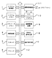
同図において、システム制御部1は、このグループ3ファクシミリ装置の各部の制御処理、および、所定のグループ3ファクシミリ伝送制御手順処理を行うものであり、システムメモリ2は、システム制御部1が実行する制御処理プログラム、および、処理プログラムを実行するときに必要な各種データなどを記憶するとともに、システム制御部1のワークエリアを構成するものであり、パラメータメモリ3は、このグループ3ファクシミリ装置に固有な各種の情報を記憶するためのものであり、時計回路4は、現在時刻情報を出力するためのものである。
【0013】
スキャナ5は、所定の解像度で原稿画像を読み取るためのものであり、プロッタ6は、所定の解像度で画像を記録出力するためのものであり、操作表示部7は、このグループ3ファクシミリ装置を操作するためのもので、各種の操作キー、および、各種の表示器からなる。
【0014】
符号化復号化部8は、画信号を符号化圧縮するとともに、符号化圧縮されている画情報を元の画信号に復号化するためのものであり、画像蓄積装置9は、符号化圧縮された状態の画情報を多数記憶するためのものである。
【0015】
グループ3ファクシミリモデム10は、グループ3ファクシミリのモデム機能を実現するためのものであり、伝送手順信号をやりとりするための低速モデム機能(V.21モデム)、および、おもに画情報をやりとりするための高速モデム機能(V.17モデム、V.34モデム、V.29モデム、V.27terモデムなど)を備えている。
【0016】
網制御装置11は、このグループ3ファクシミリ装置をアナログ公衆網PSTNに接続するためのものであり、自動発着信機能を備えている。
【0017】
これらの、システム制御部1、システムメモリ2、パラメータメモリ3、時計回路4、スキャナ5、プロッタ6、操作表示部7、符号化復号化部8、画像蓄積装置9、グループ3ファクシミリモデム10、および、網制御装置11は、内部バス12に接続されており、これらの各要素間でのデータのやりとりは、主としてこの内部バス12を介して行われている。
【0018】
また、網制御装置11とグループ3ファクシミリモデム10との間のデータのやりとりは、直接行なわれている。
【0019】
また、グループ3ファクシミリモデム10は、受信データの出力段にFIFOバッファを備えており、その出力段の構成の一例を図2に示す。ここで、FIFOバッファのデータ容量は、ECMモードの通信時に十分な値、例えば、1024〜2048オクテットに設定されている。
【0020】
同図において、受信データDTは、例えば、1オクテット(8ビット)パラレルの状態で、データFIFOバッファFFdおよび状態管理部CCに加えられている。
【0021】
データFIFOバッファFFdは、入力した1オクテットパラレルの受信データを順次転送するデータ用シフトレジスタFSdと、このデータFIFOバッファFFdが出力している先頭アドレスを管理するためのFIFOポインタデータを記憶するFIFOポインタレジスタFPを備えている。また、データ用シフトレジスタFSdの出力は、受信出力データDToとして、次段装置へ出力される。
【0022】
状態管理部CCは、受信データDTを解析して、ファクシミリ通信時のファクシミリ伝送手順信号を受信する際、ファクシミリ伝送手順信号を構成するHDLCフレーム(後述)をのどの部分を受信しているかを判断し、その判断結果をあらわすマークデータMDを出力するとともに、1つの完全なHDLCフレームを検出するとカウントアップ信号CUを出力し、また、1つの完全なHDLCフレームを外部装置へ出力すると、カウントダウン信号CDを出力し、また、外部装置より部分クリア信号PCLが加えられると、その時点で完全なHDLCフレームとして判断しているデータの先頭をあらわすように、データFIFOバッファFFdのFIFOポインタレジスタFPの値をプリセットするものである。また、状態制御部CCから出力されるマークデータMDは、制御データFIFOバッファFFcに出力され、カウントアップ信号CUおよびカウントダウン信号CDは、それぞれフレームカウンタCBに出力されている。
【0023】
制御データFIFOバッファFFcは、データFIFOバッファFFdのデータ用シフトレジスタFSdと同じシフト段数を備え、状態管理部CCより出力されるマークデータMDを順次記憶する制御データ用シフトレジスタFScからなる。
【0024】
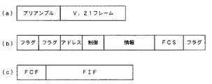
ここで、ファクシミリ伝送手順信号であるV.21フレームについて説明する。ITU−T勧告T.30によれば、バイナリ信号を運ぶV.21フレームは、図3(a)に示すように、その先頭に1秒±5%の長さのプリアンブルが設けられている。また、このプリアンブルは、所定のビットパターン(0111110)の1オクテットデータからなるフラグを、複数回連続したものである。
【0025】
また、V.21フレームは、同図(b)に示すように、HDLCフレームのフレーム構成を備えている。このHDLCフレームは、先頭に2つのフラグ、1オクテット長のアドレスフィールド、1オクテット長の制御フィールド、任意オクテット長の情報フィールド、2オクテット長のフレームチェックシーケンス(FCS;CRCデータ)、および、最後尾に1つのフラグをそれぞれ配置して構成される。
【0026】
また、V.21フレームの場合、情報フィールドには、同図(c)に示すように、ファクシミリ伝送手順信号をあらわすFCFと、当該ファクシミリ伝送手順信号に必要な情報を通知するためのFIFが配置される。
【0027】
以上の構成で、グループ3ファクシミリモデム10が受信動作するとき、グループ3ファクシミリモデム10の受信ユニット(図示略)から出力される受信データDTは、データFIFOバッファFFdのデータ用シフトレジスタFSdに順次入力されるとともに、状態管理部CCに加えられる。
【0028】
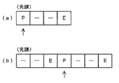
状態管理部CCは、受信データDTの内容を調べて、上述したV.21フレームの先頭に付加されているプリアンブルを検出すると、プリアンブルをあらわすマークデータMDを制御データFIFOバッファFFcへ出力し、また、V.21フレームの最後尾をあらわすフラグ(トレイルフラグ)を検出すると、最終データをあらわすマークデータMDを制御データFIFOバッファFFcへ出力する(図4(a)参照)。また、この制御データFIFOバッファFFcからの出力データは、状態管理部CCに入力される。
【0029】
また、状態管理部CCは、プリアンブルからV.21フレームの最終データまでの一連のデータを連続して検出すると、カウントアップ信号CUをフレームカウンタCBに出力し、これにより、フレームカウンタCBがカウントアップ動作し、このフレームカウンタCBから出力される受信フレーム数NBの値が増大する。
【0030】
一方、システム制御部1がグループ3ファクシミリモデム10より受信データを読み出す場合、データFIFOバッファFFdに対して受信出力データDToの読み出し動作を行う。これにより、データFIFOバッファFFdは、データ用シフトレジスタFSdより順次データを出力し、その出力されたデータは、受信出力データDToとして、システム制御部1へ出力される。
【0031】
また、状態管理部CCは、この読出動作を監視しており、データ用シフトレジスタFSdのシフト動作に応じて、制御データFIFOバッファFFcのシフト動作を行う。その結果、状態管理部CCは、制御データFIFOバッファFFcから出力されるマークデータMDを入力するので、そのマークデータMDを順次調べ、プリアンブルからV.21フレームの最終データまでの一連のマークデータMDを検出すると、カウントダウン信号CDをフレームカウンタCBに出力する。これにより、フレームカウンタCBがカウントダウン動作を行い、フレームカウンタCBから出力される受信フレーム数NBの値が減少する。
【0032】
また、受信データDTがデータ用シフトレジスタFSdに入力されるたびに、FIFOポインタレジスタFPの値のうち、受信データDTを入力すべきデータ用シフトレジスタFSdのアドレスの値が更新され、データ用シフトレジスタFSdからデータの読出が行われるたびに、FIFOポインタレジスタFPの値のうち、受信データDTを読み出すべきデータ用シフトレジスタFSdのアドレスの値が更新される。
【0033】
このようにして、グループ3ファクシミリモデム10が受信動作しているとき、フレームカウンタCBから出力される受信フレーム数NBの値は、そのときにデータFIFOバッファFFcに保存されているV.21フレームの数に等しいので、システム制御部1は、例えば、DMAチャネルを用いてグループ3ファクシミリモデム10より受信データの読出動作を行う際に、この受信フレーム数NBを読み込み、受信データを引き取るフレーム数を指定することができるので、受信データの読込動作を円滑に行うことができる。
【0034】
ところで、相手端末との間に顕著な回線遅延時間が発生する場合、次のような不具合を従来生じていた。
【0035】
例えば、図5に示すように、伝送前手順処理において、自端末よりV.21フレーム▲1▼を送出すると、このV.21フレームは、回線遅延時間tを経過した後に相手端末で受信される(V.21フレーム▲2▼)。
【0036】
ここで、漏話によるエコーが発生すると、自端末から送出したV.21フレーム▲1▼は、相手端末に到達してから回線遅延時間tを経過した時点で、自端末で受信される(V.21フレーム▲3▼)。
【0037】
一方、自端末では、V.21フレーム▲1▼の送出完了直後から受信動作に移行するため、このエコー成分であるV.21フレーム▲3▼を受信するが、図示のように、V.21フレーム▲1▼の送出を完了する前の時点からV.21フレーム▲3▼を受信している場合には、V.21フレーム▲3▼のプリアンブルの部分が欠けた状態でそれ以降のデータを受信する。
【0038】
そして、その後、相手端末からは、ファクシミリ伝送手順に従ったV.21フレーム▲4▼が送出され、このV.21フレーム▲4▼は、回線遅延時間tを経過した後に、自端末でV.21フレーム▲5▼として受信される。
【0039】
したがって、自端末におけるV.21フレーム▲1▼の送出終了した後に、相手端末からの応答信号の受信を行う場合、データFIFOバッファFFdには、V.21フレーム▲3▼の不完全なフレームの部分のデータと、V.21フレーム▲5▼の完全なフレームのデータが蓄積されるとともに、制御データFIFOバッファFFcには、図4(b)に示すように、V.21フレーム▲3▼の不完全なフレームの部分と、V.21フレーム▲5▼の完全なフレームをあらわすマークデータMDが記憶されることとなる。
【0040】
このような状態で、システム制御部1がグループ3ファクシミリモデム10より受信データの読出動作を行うと、エコー成分のV.21フレーム▲3▼の不完全な部分まで受信するので好ましくない。
【0041】
そこで、システム制御部1は、グループ3ファクシミリモデム10より受信データの読出動作を行うのに先立って、状態管理部CCに対して、部分クリア信号PCLを出力する。
【0042】
これにより、状態管理部CCは、その時点で完全なHDLCフレームとして判断しているデータの先頭をあらわすように(すなわち、最後のブロック▲5▼のプリアンブルの位置を示すように)、データFIFOバッファFFdのFIFOポインタレジスタFPの値をプリセットする。それに伴って、制御データFIFOバッファFFcの読出ポインタの値も対応する値にプリセットする。
【0043】
したがって、その後、システム制御部1がグループ3ファクシミリモデム10より受信データの読出動作を行うと、エコー成分のデータが排除された状態で、所望の受信データのみがシステム制御部1に引き取られることとなる。
【0044】
このようにして、不完全な受信データが、システム制御部1に引き取られることが抑制されるので、例えば、システム制御部1は、受信データの正当性等をチェックする必要がなく、その結果、システム制御部1の処理負担を大幅に軽減することができる。
【0045】
【発明の効果】
以上説明したように、本発明によれば、受信データを一旦FIFOバッファに蓄積した後に、出力するファクシミリモデム装置において、ファクシミリ伝送手順のV.21フレームを受信する際、上記FIFOバッファに蓄積されているV.21フレーム数を表示する手段を備えたので、外部装置が受信データを引き取る際の処理を軽減することができるという効果を得る。
【図面の簡単な説明】
【図1】本発明の一実施例にかかるグループ3ファクシミリ装置の構成例を示したブロック図。
【図2】グループ3ファクシミリモデム10の受信データ出力段の構成の一例を示したブロック図。
【図3】V.21フレームの一例を示した概略図。
【図4】制御データFIFOバッファFFcへのマークデータMDの蓄積態様を説明するための概略図。
【図5】受信時の動作を説明するためのタイムチャート。
【符号の説明】
1 システム制御部
FFd データFIFOバッファ
FSd データ用シフトレジスタ
FP FIFOポインタレジスタ
CC 状態管理部
FFc 制御データFIFOバッファ
CB フレームカウンタ[0001]
BACKGROUND OF THE INVENTION
The present invention relates to a facsimile modem apparatus that temporarily stores received data in a buffer and then outputs the data, and a facsimile apparatus including the facsimile modem apparatus.
[0002]
[Prior art]
In recent years, with the increase in the transmission speed of a facsimile, the time interval at which the host controller that controls the facsimile system collects the demodulated data output from the modem is shortened. Then, taking the demodulated data from the modem at such a short interval increases the processing load on the host controller.
[0003]
For this reason, facsimile modem devices equipped with a high data rate often have a FIFO buffer for the purpose of reducing the processing load on the host controller.
[0004]
[Problems to be solved by the invention]
By the way, the FIFO buffer can reduce the instantaneous maximum load of the host depending on the size of the buffer. However, in the control part of the facsimile transmission procedure, when demodulated data is collected via the FIFO buffer, In some cases, problems occur due to loss of real-time performance.
[0005]
The present invention has been made in view of such circumstances, and an object of the present invention is to provide a facsimile modem apparatus and a facsimile apparatus that can appropriately receive and process a facsimile transmission procedure signal.
[0006]
[Means for Solving the Problems]
The present invention relates to a facsimile modem apparatus for temporarily storing received data in a buffer and then outputting the data, wherein the received data is stored, and the stored received data is read by a next-stage apparatus, and the data A control data FIFO buffer having the same number of shift stages as that of the FIFO buffer and shifted in synchronization with the data FIFO buffer, and a flag indicating the head and tail of the data frame when receiving the data frame of the facsimile transmission procedure A series of mark data corresponding to each is generated and accumulated in the control data FIFO buffer, and when a series of data from the beginning to the last data of the data frame is continuously detected, a count up signal is output. Read from the control FIFO buffer A state management unit that generates a countdown signal each time the series of mark data detected is detected, and the number of data frames that are counted up by the countup signal and counted down by the countdown signal and accumulated in the data FIFO buffer And a frame counter that outputs the number of data frames .
[0007]
In addition, the state management unit, in response to a command from an external device, instructs the start of the latest data frame stored in the data FIFO buffer, the value of the read pointer of the data FIFO buffer, and the control The value of the read pointer of the data FIFO buffer is updated.
[0008]
A facsimile apparatus comprising the facsimile modem apparatus according to
[0010]
DETAILED DESCRIPTION OF THE INVENTION
Hereinafter, embodiments of the present invention will be described in detail with reference to the accompanying drawings.
[0011]
FIG. 1 shows a
[0012]
In the figure, a
[0013]
The
[0014]
The encoding / decoding unit 8 encodes and compresses the image signal, and also decodes the encoded and compressed image information into the original image signal. The image storage device 9 performs encoding and compression. This is for storing a large number of image information in the selected state.
[0015]
The
[0016]
The network control apparatus 11 is for connecting the
[0017]
The
[0018]
Data exchange between the network control device 11 and the
[0019]
Further, the
[0020]
In the figure, received data DT is added to the data FIFO buffer FFd and the state management unit CC in a 1-octet (8-bit) parallel state, for example.
[0021]
The data FIFO buffer FFd is a data shift register FSd that sequentially transfers input 1-octet parallel received data, and a FIFO pointer that stores FIFO pointer data for managing the head address output by the data FIFO buffer FFd. A register FP is provided. The output of the data shift register FSd is output to the next stage device as reception output data DTo.
[0022]
The state management unit CC analyzes the received data DT and determines which part of the HDLC frame (described later) constituting the facsimile transmission procedure signal is received when receiving the facsimile transmission procedure signal at the time of facsimile communication. In addition, the mark data MD representing the determination result is output, and when one complete HDLC frame is detected, the count-up signal CU is output, and when one complete HDLC frame is output to the external device, the count-down signal CD is output. When the partial clear signal PCL is applied from the external device, the value of the FIFO pointer register FP of the data FIFO buffer FFd is set so as to indicate the head of the data determined as a complete HDLC frame at that time. It is something to be preset. Further, the mark data MD output from the state control unit CC is output to the control data FIFO buffer FFc, and the count up signal CU and the count down signal CD are output to the frame counter CB, respectively.
[0023]
The control data FIFO buffer FFc has the same number of shift stages as the data shift register FSd of the data FIFO buffer FFd, and includes a control data shift register FSc that sequentially stores the mark data MD output from the state management unit CC.
[0024]
Here, V. which is a facsimile transmission procedure signal. 21 frames will be described. ITU-T recommendation 30 according to V.30 carrying a binary signal. As shown in FIG. 3A, 21 frames are provided with a preamble having a length of 1 second ± 5% at the head thereof. In addition, this preamble is a flag in which a flag composed of one octet data of a predetermined bit pattern (0111110) is continued a plurality of times.
[0025]
V. The 21 frame has a frame configuration of an HDLC frame as shown in FIG. This HDLC frame has two flags at the beginning, an address field of 1 octet length, a control field of 1 octet length, an information field of arbitrary octet length, a frame check sequence (FCS; CRC data) of octet length, and a tail Are configured by arranging one flag respectively.
[0026]
V. In the case of 21 frames, as shown in FIG. 6C, an FCF representing a facsimile transmission procedure signal and an FIF for notifying information necessary for the facsimile transmission procedure signal are arranged in the information field.
[0027]
With the above configuration, when the
[0028]
The state management unit CC examines the contents of the received data DT, and the above-described V.D. When the preamble added to the head of the 21th frame is detected, the mark data MD representing the preamble is output to the control data FIFO buffer FFc. When a flag (trailing flag) representing the end of 21 frames is detected, mark data MD representing the final data is output to the control data FIFO buffer FFc (see FIG. 4A). The output data from the control data FIFO buffer FFc is input to the state management unit CC.
[0029]
In addition, the state management unit CC receives the V.V. When a series of data up to the final data of 21 frames is continuously detected, a count-up signal CU is output to the frame counter CB, whereby the frame counter CB performs a count-up operation, and the reception output from the frame counter CB is received. The value of the number of frames NB increases.
[0030]
On the other hand, when the
[0031]
Further, the state management unit CC monitors the read operation, and performs the shift operation of the control data FIFO buffer FFc in accordance with the shift operation of the data shift register FSd. As a result, since the state management unit CC receives the mark data MD output from the control data FIFO buffer FFc, the state management unit CC sequentially examines the mark data MD, and the V.V. When a series of mark data MD up to the final data of 21 frames is detected, a countdown signal CD is output to the frame counter CB. As a result, the frame counter CB performs a countdown operation, and the value of the number of received frames NB output from the frame counter CB decreases.
[0032]
Further, each time the reception data DT is input to the data shift register FSd, the value of the address of the data shift register FSd to which the reception data DT is to be input is updated among the values of the FIFO pointer register FP. Each time data is read from the register FSd, the value of the address of the data shift register FSd from which the received data DT is to be read out of the value of the FIFO pointer register FP is updated.
[0033]
In this way, when the
[0034]
By the way, when a remarkable line delay time occurs with a partner terminal, the following problems have conventionally occurred.
[0035]
For example, as shown in FIG. When 21 frames (1) are transmitted, this V.V. The 21 frame is received by the partner terminal after the line delay time t has elapsed (V.21 frame (2)).
[0036]
Here, when an echo due to crosstalk occurs, the V.V. The 21 frame {circle around (1)} is received by the own terminal when the line delay time t has elapsed after reaching the counterpart terminal (V.21 frame {circle around (3)}).
[0037]
On the other hand, in its own terminal, V.I. Since the transition to the receiving operation starts immediately after the completion of the transmission of 21 frames (1), V. 21 frames (3) are received. From the point in time before transmission of 21 frames {circle around (1)} is completed. If 21 frames (3) are received, The subsequent data is received in a state where the preamble portion of 21 frame (3) is missing.
[0038]
Then, from the other terminal, V.P. 21 frames (4) are sent out. 21 frame {circle around (4)} is received by the terminal itself after the line delay time t has elapsed. Received as 21 frames (5).
[0039]
Therefore, the V.V. When receiving a response signal from the partner terminal after the transmission of 21 frames (1) is completed, the data FIFO buffer FFd contains V. The data of the incomplete frame portion of 21 frames (3), The complete frame data of 21 frames (5) is accumulated, and the control data FIFO buffer FFc stores V.V. as shown in FIG. 21. Incomplete frame portion of frame (3); Mark data MD representing a complete frame of 21 frames (5) is stored.
[0040]
In this state, when the
[0041]
Therefore, the
[0042]
As a result, the state management unit CC indicates the beginning of the data determined as a complete HDLC frame at that time (that is, indicates the position of the preamble of the last block (5)) , and the data FIFO buffer. The value of the FIFO pointer register FP of FFd is preset. Along with this, the value of the read pointer of the control data FIFO buffer FFc is also preset to a corresponding value.
[0043]
Therefore, after that, when the
[0044]
In this way, since incomplete received data is suppressed from being taken over by the
[0045]
【The invention's effect】
As described above, according to the present invention, the received data is temporarily stored in the FIFO buffer and then output in the facsimile modem apparatus which outputs the received data in the facsimile transmission procedure. When receiving 21 frames, the V.V. stored in the FIFO buffer is received. Since the means for displaying the number of 21 frames is provided, it is possible to reduce the processing when the external device collects the received data.
[Brief description of the drawings]
FIG. 1 is a block diagram showing a configuration example of a
FIG. 2 is a block diagram showing an example of a configuration of a received data output stage of the
FIG. Schematic which showed an example of 21 frames.
FIG. 4 is a schematic diagram for explaining an accumulation mode of mark data MD in a control data FIFO buffer FFc.
FIG. 5 is a time chart for explaining an operation at the time of reception.
[Explanation of symbols]
1 System control unit FFd Data FIFO buffer FSd Data shift register FP FIFO pointer register CC State management unit FFc Control data FIFO buffer CB Frame counter
Claims (3)
受信データが蓄積されるとともに、蓄積された受信データが次段装置により読み出されるデータFIFOバッファと、
前記データFIFOバッファと同一のシフト段数を有するとともに、前記データFIFOバッファと同期してシフト動作される制御データFIFOバッファと、
ファクシミリ伝送手順のデータフレームを受信する際、データフレームの先頭と最後尾をあらわすフラグを検出し、それぞれに対応した一連のマークデータを発生して前記制御データFIFOバッファへ蓄積し、前記データフレームの先頭から最終データまでの一連のデータを連続して検出するとカウントアップ信号を出力し、前記制御FIFOバッファから読み出される前記一連のマークデータを検出するたびにカウントダウン信号を発生する状態管理部と、
前記カウントアップ信号によりカウントアップするとともに、前記カウントダウン信号によりカウントダウンし、前記データFIFOバッファに蓄積されるデータフレーム数を計数し、当該データフレーム数を出力するフレームカウンタを備えたことを特徴とするファクシミリモデム装置。A facsimile modem device for outputting received data once after storing it in a buffer ,
A data FIFO buffer in which received data is accumulated and the accumulated received data is read out by the next-stage device;
A control data FIFO buffer having the same number of shift stages as the data FIFO buffer and shifted in synchronization with the data FIFO buffer;
When receiving a data frame of a facsimile transmission procedure, a flag representing the beginning and end of the data frame is detected, a series of mark data corresponding to each is generated, stored in the control data FIFO buffer, and the data frame A state management unit that outputs a count-up signal when a series of data from the beginning to the last data is continuously detected, and generates a count-down signal each time the series of mark data read from the control FIFO buffer is detected;
A facsimile comprising a frame counter that counts up by the count up signal, counts down by the count down signal, counts the number of data frames stored in the data FIFO buffer, and outputs the number of data frames Modem device.
Priority Applications (1)
| Application Number | Priority Date | Filing Date | Title |
|---|---|---|---|
| JP2001355164A JP4053285B2 (en) | 2001-11-20 | 2001-11-20 | Facsimile modem apparatus and facsimile apparatus |
Applications Claiming Priority (1)
| Application Number | Priority Date | Filing Date | Title |
|---|---|---|---|
| JP2001355164A JP4053285B2 (en) | 2001-11-20 | 2001-11-20 | Facsimile modem apparatus and facsimile apparatus |
Publications (2)
| Publication Number | Publication Date |
|---|---|
| JP2003158617A JP2003158617A (en) | 2003-05-30 |
| JP4053285B2 true JP4053285B2 (en) | 2008-02-27 |
Family
ID=19166909
Family Applications (1)
| Application Number | Title | Priority Date | Filing Date |
|---|---|---|---|
| JP2001355164A Expired - Fee Related JP4053285B2 (en) | 2001-11-20 | 2001-11-20 | Facsimile modem apparatus and facsimile apparatus |
Country Status (1)
| Country | Link |
|---|---|
| JP (1) | JP4053285B2 (en) |
-
2001
- 2001-11-20 JP JP2001355164A patent/JP4053285B2/en not_active Expired - Fee Related
Also Published As
| Publication number | Publication date |
|---|---|
| JP2003158617A (en) | 2003-05-30 |
Similar Documents
| Publication | Publication Date | Title |
|---|---|---|
| US4841373A (en) | Facsimile transmission control method in which a frame of stored image data is transmitted when either a predetermined time has elapsed or a predetermined amount of image data has been stored | |
| JPH02268066A (en) | facsimile machine | |
| US5933247A (en) | Image communication apparatus capable of parallel processing of image storage and transmission | |
| JP3206648B2 (en) | Multi-function peripheral | |
| JP4053285B2 (en) | Facsimile modem apparatus and facsimile apparatus | |
| JPH01119176A (en) | Data transmission system | |
| JPS60163570A (en) | fax machine | |
| JP3059745B2 (en) | Facsimile apparatus and control method thereof | |
| JP3222576B2 (en) | Encoding device | |
| JP3264559B2 (en) | Image coding method and apparatus | |
| JP4008831B2 (en) | Image information storage device and control method thereof | |
| JP3008893B2 (en) | Packet multiplexing apparatus and method | |
| JP2672174B2 (en) | Facsimile machine | |
| JP2945017B2 (en) | Control system for facsimile machine | |
| JPS6374262A (en) | facsimile communication system | |
| JPS62157461A (en) | Bulk transmission method for the same destination in sequential broadcasting | |
| JP2790820B2 (en) | Facsimile communication method | |
| JP2689745B2 (en) | Coded data transmission processing method | |
| JP2000138837A (en) | Image information processing device | |
| JPH04336755A (en) | facsimile machine | |
| JPS5994966A (en) | Picture data compressing device | |
| JPH053781B2 (en) | ||
| JP2002330272A (en) | Facsimile machine | |
| JPH077589A (en) | Transmission control method for facsimile machine | |
| JPH01286547A (en) | Data transmission system |
Legal Events
| Date | Code | Title | Description |
|---|---|---|---|
| A621 | Written request for application examination |
Free format text: JAPANESE INTERMEDIATE CODE: A621 Effective date: 20040721 |
|
| A977 | Report on retrieval |
Free format text: JAPANESE INTERMEDIATE CODE: A971007 Effective date: 20051111 |
|
| A131 | Notification of reasons for refusal |
Free format text: JAPANESE INTERMEDIATE CODE: A131 Effective date: 20051122 |
|
| A521 | Written amendment |
Free format text: JAPANESE INTERMEDIATE CODE: A523 Effective date: 20060123 |
|
| A131 | Notification of reasons for refusal |
Free format text: JAPANESE INTERMEDIATE CODE: A131 Effective date: 20061031 |
|
| A521 | Written amendment |
Free format text: JAPANESE INTERMEDIATE CODE: A523 Effective date: 20061225 |
|
| A131 | Notification of reasons for refusal |
Free format text: JAPANESE INTERMEDIATE CODE: A131 Effective date: 20070612 |
|
| A521 | Written amendment |
Free format text: JAPANESE INTERMEDIATE CODE: A523 Effective date: 20070808 |
|
| A02 | Decision of refusal |
Free format text: JAPANESE INTERMEDIATE CODE: A02 Effective date: 20070904 |
|
| A521 | Written amendment |
Free format text: JAPANESE INTERMEDIATE CODE: A523 Effective date: 20071029 |
|
| A911 | Transfer to examiner for re-examination before appeal (zenchi) |
Free format text: JAPANESE INTERMEDIATE CODE: A911 Effective date: 20071112 |
|
| TRDD | Decision of grant or rejection written | ||
| A01 | Written decision to grant a patent or to grant a registration (utility model) |
Free format text: JAPANESE INTERMEDIATE CODE: A01 Effective date: 20071204 |
|
| A61 | First payment of annual fees (during grant procedure) |
Free format text: JAPANESE INTERMEDIATE CODE: A61 Effective date: 20071205 |
|
| FPAY | Renewal fee payment (event date is renewal date of database) |
Free format text: PAYMENT UNTIL: 20101214 Year of fee payment: 3 |
|
| R150 | Certificate of patent or registration of utility model |
Ref document number: 4053285 Country of ref document: JP Free format text: JAPANESE INTERMEDIATE CODE: R150 Free format text: JAPANESE INTERMEDIATE CODE: R150 |
|
| FPAY | Renewal fee payment (event date is renewal date of database) |
Free format text: PAYMENT UNTIL: 20101214 Year of fee payment: 3 |
|
| FPAY | Renewal fee payment (event date is renewal date of database) |
Free format text: PAYMENT UNTIL: 20111214 Year of fee payment: 4 |
|
| FPAY | Renewal fee payment (event date is renewal date of database) |
Free format text: PAYMENT UNTIL: 20111214 Year of fee payment: 4 |
|
| FPAY | Renewal fee payment (event date is renewal date of database) |
Free format text: PAYMENT UNTIL: 20121214 Year of fee payment: 5 |
|
| FPAY | Renewal fee payment (event date is renewal date of database) |
Free format text: PAYMENT UNTIL: 20131214 Year of fee payment: 6 |
|
| LAPS | Cancellation because of no payment of annual fees |