JP4098024B2 - Laser spot welding method - Google Patents
Laser spot welding method Download PDFInfo
- Publication number
- JP4098024B2 JP4098024B2 JP2002223866A JP2002223866A JP4098024B2 JP 4098024 B2 JP4098024 B2 JP 4098024B2 JP 2002223866 A JP2002223866 A JP 2002223866A JP 2002223866 A JP2002223866 A JP 2002223866A JP 4098024 B2 JP4098024 B2 JP 4098024B2
- Authority
- JP
- Japan
- Prior art keywords
- laser beam
- laser
- light
- irradiation
- processing point
- Prior art date
- Legal status (The legal status is an assumption and is not a legal conclusion. Google has not performed a legal analysis and makes no representation as to the accuracy of the status listed.)
- Expired - Fee Related
Links
Images

Landscapes
- Laser Beam Processing (AREA)
Description
【0001】
【発明の属する利用分野】
本発明は難加工材料に好適に適用できるレーザスポット溶接方法に関する。
【0002】
【従来の技術】
高反射率材料である純銅や純アルミのレーザ接合技術は、近い将来に非常に重要な技術のひとつになると考えられる。純銅と純銅の接合の応用分野として電子部品間の半田に代わる半田フリー技術として期待できる。これはリサイクルの観点からも、半田を取り除く工程が不要になるので、コスト・環境に対しても有利な技術といえる。一方、アルミの接合も、リサイクルおよび軽量化の観点から、様々な分野に利用さている。具体的には、従来から自動車のシャーシや車載部品への応用が進められており、近年、電子機器分野(代表例として、携帯電話の電池の外装材等)へも応用が開始されている。
【0003】
一般にレーザ溶接に用いられるレーザは、炭酸ガスレーザ(波長:10.6μm)や基本波YAGレーザ(波長:1.064μm)で、これらの波長はいずれも近赤外線領域にある。純銅、純アルミ等の高反射率材料に対するこれらの波長帯の光の反射率は99%以上であり、これらのレーザ光はほとんど吸収されない。換言すれば、炭素鋼、ニッケル等のレーザ溶接が一般的に適用される材料に比べて高反射率材料のレーザ光の吸収率は一桁以上も低い。さらにこれら高反射率材料の熱伝導率は、炭素鋼、ステンレス鋼等のレーザ溶接が一般的に適用される材料の熱伝導率の2倍以上も高い。このことは、高反射率材料では加工部に高い加工エネルギーを投入し、溶融させることが難しいことを示している。
【0004】
加工エネルギーを投入し、溶融させることが困難であるという課題に対しては、レーザ発振形態の異なる2種類のレーザ光を加工点に同時に照射し、第1のレーザ光よりもエネルギー密度が高く、照射時間が短い第2のレーザ光で穴加工を行うと同時に、第1のレーザ光をこの穴内で多重散乱させることにより穴内に閉じ込めることで、レーザ加工効率を向上させるレーザ溶接方法が用いられている。この溶接方法によれば、投入できるエネルギー量を改善することが可能である。
【0005】
しかし、一旦これらの材料が加熱され溶融が開始すると、吸収率が増加するため、一気に加工が進んでしまうという別の考慮すべき面も存在する。これらの理由から、純銅、純アルミに対するレーザ加工では、非常に安定した加工品質を維持するのが難しい。特に、マイクロ領域(約φ2mm以下)の溶接加工では、これらの課題が顕著化してしまう。
【0006】
【発明が解決しようとする課題】
純銅、純アルミ等の高反射率材料のレーザ溶接方法における課題として2点挙げられる。
【0007】
1つ目の課題は、レーザ光の波長に対して高反射率の材料(難加工材料)に対して、発振形態の異なる2種類のレーザ光を加工点で空間的、時間的に一致するように照射するレーザ溶接方法では、投入するエネルギー量が大きいという点である。例えば純銅に溶融深さ2百μm程度の溶融部を形成するためには数J程度のエネルギーを投入する必要がある。これに対して、炭素鋼、ステンレス等に深さ2百μmの溶融部を形成するために必要な投入エネルギーは数十mJ〜数百mJである。このように、高反射率材料に対するレーザ溶接方法は、投入エネルギーに対する加工効率が悪い。このような加工性悪さを改善するには、単純にレーザ光照射時間を大きくしたり、エネルギー密度を上げたりするだけでは十分でない。その理由としては、次のような問題があるからである。レーザ光照射時間を増加させた場合、加工部周辺への熱影響や加工領域の酸化が生じる。また、エネルギー密度を上げた場合、僅かな加工表面状態の違いによって加工点での溶融の開始時間が変化すると、加工ばらつきが大きくなり、加工品質を一定に保つことが難しい。さらに、投入エネルギーが大きすぎると、溶融材料が吹き飛んでしまい、加工後に穴が埋まらず接合されない加工不良であるアンダーフィルドスポットウェルドの発生確率が増大するので、やみくもにエネルギー密度を増大させることはできない。
【0008】
2つ目の課題は、純銅や純アルミ等の高反射率材料は、溶融させるには高いピークパワーが必要であるが、一旦溶融すると反射率が急激に低下し吸収率が増加するため、高いピークパワーのままであると一気に加工が進んでしまうという点である。この課題に対しては、上述した異なる2種類のレーザを用いた従来の加工方法では解決できず、加工品質を一定に保つことが難しく、新たな工夫が必要である。
【0009】
以上のように、高反射率材料に対してマイクロスポットレーザ溶接を実施するには、投入エネルギーに対する加工効率の向上と、レーザのピークパワーが高い状態で溶融のための吸収率が増加することに起因する課題とを解決する必要がある。特にマイクロ領域の加工ではこれらの課題が顕在化し、加工を不安定にさせる大きな要因となっている。
【0010】
本発明は、上記の従来の課題を解決し、投入エネルギーに対する加工効率が向上し、レーザのピークパワーが高い状態で溶融のための吸収率が増加することに起因する加工品質の不安定が解消できるレーザスポット溶接方法を提供することを目的とする。
【0011】
【課題を解決するための手段】
本発明は上記の目的を達成するために以下のように構成される。
【0012】
本発明のレーザスポット溶接方法は、第1及び第2のレーザ光のスポットを被加工物の加工点に一致させるレーザスポット溶接方法であって、前記第1のレーザ光を照射中に、前記第1のレーザ光よりもエネルギー密度が高く照射時間が短いパルス状の第2のレーザ光を前記加工点に照射し、次いで、前記第1のレーザ光を単独で前記加工点に照射することにより、前記被加工物に穴を形成し、前記穴内で前記第1のレーザ光を多重散乱させて前記被加工物材料を溶融せしめる。
第1のレーザスポット溶接方法では、前記第2のレーザ光の照射期間終了後で前記加工点からの正反射光の強度が増加し始めた時に、前記第1のレーザ光のエネルギー密度を最大とする。
第2のレーザスポット溶接方法では、前記加工点からの正反射光を計測し、正反射光の強度変化に基づいて前記被加工物材料が溶融したことを検知し、前記第1のレーザ光のエネルギー密度と照射時間とを制御する。
第3のレーザスポット溶接方法では、前記第2のレーザ光の照射期間終了後に、前記第1のレーザ光を単独で照射中に前記加工点からの近赤外線を計測し、前記近赤外線の変化に基づいて前記第1のレーザ光の照射を停止する。
【0016】
【発明の実施の形態】
本発明のレーザスポット溶接方法では、第1のレーザ光と、これよりもエネルギー密度が高く照射時間が短いパルス状の第2のレーザ光とを同時に加工点に照射し、被加工物に穴を形成し、穴内で第1のレーザ光を多重散乱させる。これにより、高反射率材料に対する加工効率の向上を図る。一方、高反射率材料料に関するレーザのピークパワーが高い状態で溶融のための吸収率が増加することに起因する問題に関しては、第2のレーザ光を照射した後、第1のレーザ光を単独で照射することで解決を図る。
【0017】
本発明者らは、高反射率材料の溶接加工における上述した問題は、溶接プロセスのどの段階でエネルギーをどの程度投入するかに強く起因していると考えた。つまり、溶融部が形成される前又は形成途中にどれだけのエネルギーを投入するか、また、溶融部が形成された後にどれだけのエネルギーを投入するかに起因していると考えた。溶融部の形成前及び形成途中の段階では、反射率が低いため、第1のレーザ光に加えてエネルギー密度が高い第2のレーザ光を照射する。しかしながら、溶融部が形成されると、反射率および熱伝導率が急激に減少するため加工性が向上する。その時点で第1及び第2のレーザ光を照射し続けると、投入エネルギーが過剰となるので、アンダーフィルドスポットウェルドのように溶融材料が吹き飛んでしまう欠陥が発生する。従って、溶融部が形成された後は、第1のレーザ光を単独で照射することにより、投入エネルギーを減少させ、加工の進行を抑える。これにより、高反射率材料の溶接加工においても、深い溶け込みが得られ、アンダーフィルドスポットウェルドのような加工不良の発生を防止して、加工品質を安定させることが可能になる。
【0018】
本発明のレーザスポット溶接方法において、前記パルス状の第2のレーザ光の照射期間内に投入される前記第1のレーザ光によるエネルギー量より、前記第2のレーザ光の照射期間終了後に投入される前記第1のレーザ光によるエネルギー量が大きいことが好ましい。上述した通り、溶融後は、高反射率材料の反射率は急激に低下するので、被加工物内に蓄熱するのが容易になる。従って、溶融部の形成途中にエネルギーを投入するよりも、溶融部形成後にエネルギーを投入する方が、投入エネルギーに対する加工効率は向上する。よって、かかる好ましい構成により、少ない投入エネルギーで効率よく高反射率材料の溶接加工を行うことができる。
【0019】
本発明の第1のレーザスポット溶接方法では、前記第2のレーザ光の照射期間終了後に前記第1のレーザ光を単独で照射中に、前記加工点からの正反射光の強度が増加し始めた時に、前記第1のレーザ光のエネルギー密度を最大とする。これにより、投入エネルギーに対する加工効率はより一層向上する。
ここで、レーザ光のエネルギー密度dE(単位:W/m2)とは、レーザ光の投入エネルギーをE(単位:J)、照射時間をT(単位:s)、照射面積をS(単位:m2)としたとき、dE=(E/T)/Sで表される。ここで、E/Tはレーザピークパワーと呼ばれる。
【0020】
また、本発明の第2のレーザスポット溶接方法では、前記加工点からの正反射光を計測し、正反射光の強度変化に基づいて前記被加工物材料が溶融したことを検知し、前記第1のレーザ光のエネルギー密度と照射時間とを制御する。一般に、加工点からの反射光強度は、加工開始後キーホールが形成(即ち、溶融部が形成)されるまでの間は逓減し、その後、逓増する傾向がある。従って、反射光の変化から被加工物材料が溶融したことを検知し、第1のレーザ光のエネルギー密度と照射時間とを制御することにより、投入エネルギーに対する加工効率を向上させることができる。
【0021】
また、本発明の第3のレーザスポット溶接方法では、前記第2のレーザ光の照射期間終了後に、前記第1のレーザ光を単独で照射中に前記加工点からの近赤外線を計測し、前記近赤外線の変化に基づいて前記第1のレーザ光の照射を停止する。本発明者らは加工表面の酸化の進行と加工点からの近赤外線の強度との間には関連性があることを見いだした。従って、かかる構成により、加工部の酸化を抑制することができる。
【0024】
以下、本発明を実施の形態を用いて説明する。
【0025】
(実施の形態1)
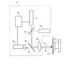
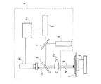
図1は、本発明の実施の形態1にかかるレーザスポット溶接装置1の概略構成図である。図1中、2は被加工物(例えば純銅)3の板を載置し、その位置を制御するXYZステージである。5は波長532nmのレーザ光(第2のレーザ光)4を発生するAOQスイッチ第2高調波YAGレーザ発振器、7は波長1064nmのレーザ光(第1のレーザ光)6を発生する基本波YAGパルスレーザ発振器である。8は、波長532nmのレーザ光4を反射し、波長1064nmのレーザ光6を透過させる誘電体コートが施されたミラー、9は、波長532nmのレーザ光4と波長1064nmのレーザ光6とを95%反射し、これら以外の波長の光を透過させる誘電体コートが施されたミラーである。10は集光レンズ、12は正反射光11のうち波長1064nmの光を計測するフォトセンサ、13はレーザ発振器7を制御する制御装置である。
【0026】
[実施例1]
図1の装置を用いて30mm×40mm×100μm厚の純銅からなる被加工物3に溶融部を形成した。
【0027】
レーザ発振器5から出射した波長532nmの第2高調波YAGレーザ光4とレーザ発振器7から出射した波長1064nmの基本波YAGレーザ光6とをミラー8に入射させ、レーザ光4を反射させ、レーザ光6を透過させて、2つのレーザ光4,6の光軸を揃えた。レーザ光4,6をミラー9で反射させ、集光レンズ10で集光して、純銅3の加工点で各レーザ光のスポットを空間的に一致するように照射した。レーザ光4のスポット径は30μm、レーザ光6のスポット径は150μmとした。
【0028】
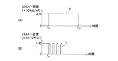
図2(A),図2(B)は、それぞれレーザ光6及びレーザ光4の波形図である。図2(A),図2(B)の横軸は時間、縦軸はエネルギー密度をそれぞれ示す。図2(A),図2(B)に示すように時刻t0〜時刻t10の間の10ms間に基本波YAGレーザ光6を投入エネルギー7.5Jで照射した。レーザ光6のエネルギー密度は4.24×10⁷(kW/m2)で一定とした。基本波YAGレーザ光6の照射開始と同時に、エネルギー密度1.45×1010(kW/m2)の第2高調波YAGレーザ光4をパルス幅78nsで1kHz繰り返しで4回、投入エネルギー0.8mJで照射した。
【0029】
レーザ光4を照射することにより純銅3の表面に直径30μm程度の穴が形成され、レーザ光4の照射後、レーザ光6が該穴内で多重散乱して溶融部が形成された。得られた溶融部径は177μmであり、アンダーフィルドスポットウェルドのような加工不良が発生することなく、深い溶け込みが得られた。
【0030】
比較例として、基本波YAGレーザ光6の照射条件を投入エネルギー7.5Jで4msとする以外は上記と同様にした。その結果、溶融部径は80μm程度であった。従って、本実施例1により、効率よく良好な溶け込み形状を得ることができた。
【0031】
[実施例2]
本実施例2が実施例1と相違するのは、波長1064nmの基本波YAGレーザ光6の照射条件を以下のように変更した点のみである。
【0032】
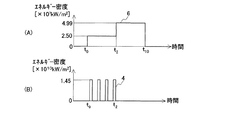
図3(A),図3(B)は、それぞれレーザ光6及びレーザ光4の波形図である。図3(A),図3(B)の横軸は時間、縦軸はエネルギー密度をそれぞれ示す。図3(A),図3(B)に示すように時刻t0〜時刻t10の間の10ms間に基本波YAGレーザ光6を投入エネルギー7.5Jで照射した。基本波YAGレーザ光6の照射開始と同時に、エネルギー密度1.45×10¹⁰(kW/m2)の第2高調波YAGレーザ光4をパルス幅78nsで1kHz繰り返しで4回、投入エネルギー0.8mJで照射した。レーザ光6は、レーザ光4が照射される時刻t0〜時刻t2の期間(3ms)内に全投入エネルギー7.5Jのうちの1.7割に相当する1.3Jを、レーザ光4の照射期間終了後の時刻t2〜時刻t10の期間(7ms)内に残りの8.1割に相当する6.1Jを投入した。レーザ光6のエネルギー密度は、時刻t0〜時刻t2の間は2.50×107(kW/m2)で一定とし、時刻t2〜時刻t10の間は4.99×107(kW/m2)で一定とした。
【0033】
レーザ光4を照射することにより純銅3の表面に直径30μm程度の穴が形成され、レーザ光4の照射後、レーザ光6が該穴内で多重散乱して溶融部が形成された。得られた溶融部径は281μmであり、実施例1より効率よく溶融部を形成することができた。また、溶融部は厚さ100μmの純銅3の裏面(レーザ光の入射側とは反対側の面)まで達し、裏面での溶融部径は186μmであった。また、実施例1と同様にアンダーフィルドスポットウェルドのような加工不良が発生することなく、深い溶け込みが得られた。
【0034】
[実施例3]
本実施例3が実施例1と相違するのは、純銅3の加工点からの正反射光を測定し、正反射光の強度変化に基づいて純銅3が溶融したことを検知し、基本波YAGレーザ光6のエネルギー密度と照射時間を制御した点、及び、波長1064nmの基本波YAGレーザ光6の照射条件を以下のように変更した点のみである。
【0035】
図1に示す装置を用い、純銅3の加工点での正反射光11を集光レンズ10を通過させ、更にその一部をミラー9を透過させてフォトセンサ12に入射させた。フォトセンサ12は、正反射光11のうち波長1064nmの光の強度に応じた信号を出力し、制御装置13は、この信号強度に応じてレーザ発振器7を制御して、これから出射される波長1064nmのレーザ光6のエネルギー密度と照射時間が調整されるように設定されている。
【0036】
図4(A),図4(B)は、それぞれレーザ光6及びレーザ光4の波形図である。図4(A),図4(B)の横軸は時間、縦軸はエネルギー密度をそれぞれ示す。図4(A),図4(B)に示すように時刻t0〜時刻t10の間の10ms間に基本波YAGレーザ光6を投入エネルギー7.5Jで照射した。基本波YAGレーザ光6の照射開始と同時に、エネルギー密度1.45×10¹⁰(kW/m2)の第2高調波YAGレーザ光4をパルス幅78nsで1kHz繰り返しで4回、投入エネルギー0.8mJで照射した。
【0037】
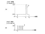
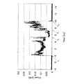
図5にフォトセンサ12で検出された波長1064nmの反射光強度を示す。図5において、横軸は時間、縦軸は正反射光11の強度である。正反射光11の強度は、時刻t0でレーザ光4,6の照射を開始した後徐々に減衰し、レーザ光4の照射が終了した後の時刻t4〜時刻t5の約2ms間一定の値になってから、時刻t5で再び増加し始めた。この正反射光11の変化をフォトセンサー12で検知し、正反射光11が増加し始めた時刻t5(レーザ光の照射開始から7ms経過した時)に、レーザ光6のエネルギー密度を増加させた。即ち、図4(A)に示すように、時刻t5にレーザ光6のエネルギー密度を13.1×10⁷(kW/m2)に上昇させ、時刻t5から1msの間に、レーザ光6の全投入エネルギー7.5Jの3.1割に相当する2.32Jを投入した。この期間以外のレーザ光6のエネルギー密度は3.26×107(kW/m2)で一定とした。
【0038】
得られた溶融部径は、レーザ光の入射側の面で272μm、レーザ光の出射側の面で188μmであった。実施例2に比べて、溶融部径の表裏の差が小さくなり(即ち、溶融部のテーパ角度が小さくなり)、溶融部形状が改善された。また、実施例1と同様にアンダーフィルドスポットウェルドのような加工不良が発生することなく、深い溶け込みが得られた。
【0039】
(実施の形態2)
図6は、本発明の実施の形態2にかかるレーザスポット溶接装置14の概略構成図である。図6中、2は被加工物(例えば純銅)3の板を載置し、その位置を制御するXYZステージである。5は波長532nmのレーザ光(第2のレーザ光)4を発生するAOQスイッチ第2高調波YAGレーザ発振器、7は波長1064nmのレーザ光(第1のレーザ光)6を発生する基本波YAGパルスレーザ発振器である。8は、波長532nmのレーザ光4を反射し、波長1064nmのレーザ光6を透過させる誘電体コートが施されたミラー、15は、波長532nmのレーザ光4と波長1064nmのレーザ光6とを反射し、波長1.25μm以上の近赤外光を透過させる誘電体コートが施されたミラーである。10は集光レンズ、17は加工点から出射し、集光レンズ10及びミラー15を透過した波長1.55μmの近赤外光16を計測するInGaAsのフォトセンサ、18はレーザ発振器7を制御する制御装置である。
【0040】
[実施例4]
図6の装置を用いて30mm×40mm×200μm厚の純銅からなる被加工物3に溶融部を形成した。
【0041】
レーザ発振器5から出射した波長532nmの第2高調波YAGレーザ光4とレーザ発振器7から出射した波長1064nmの基本波YAGレーザ光6とをミラー8に入射させ、レーザ光4を反射させ、レーザ光6を透過させて、2つのレーザ光4,6の光軸を揃えた。レーザ光4,6をミラー15で反射させ、集光レンズ10で集光して、純銅3の加工点で各レーザ光のスポットを空間的に一致するように照射した。レーザ光4のスポット径は30μm、レーザ光6のスポット径は150μmとした。
【0042】
図7(A),図7(B)は、それぞれレーザ光6及びレーザ光4の波形図である。図7(A),図7(B)の横軸は時間、縦軸はエネルギー密度をそれぞれ示す。図7(A),図7(B)に示すように時刻t0〜時刻t10の間の20ms間に基本波YAGレーザ光6を投入エネルギー20Jで照射した。レーザ光6のエネルギー密度は5.66×10⁷(kW/m2)で一定とした。基本波YAGレーザ光6の照射開始と同時に、エネルギー密度1.45×1010(kW/m2)の第2高調波YAGレーザ光4をパルス幅78nsで1kHz繰り返しで7回、投入エネルギー0.8mJで照射した。加工点から出射した波長1.55μmの近赤外光16を集光レンズ10、ミラー15を順に透過させてフォトセンサ17に入射させた。
【0043】
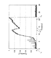
フォトセンサ17により計測された近赤外光16の強度を図8に示す。図8において、横軸は時間、縦軸は近赤外光16の正規化された強度である。図8に示すように、近赤外光16はレーザ光4,6の照射を開始した時刻t0から12ms経過した時刻t6まで増加し、その後、約2msの間減少し、時刻t7から再び増加に転じた。
【0044】
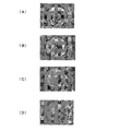
図9(A)、図9(B)、図9(C)、図9(D)は、レーザ光6の照射時間を順に10ms、12ms、14ms、20msとした以外は図7(A),図7(B)と同じ条件でレーザ光4,6を照射したときの純銅3のレーザ光照射側の面の加工部を写した写真である。これらから、図9(C)の14ms程度で加工を終了したとき、加工形状、表面の溶融状態、および加工部周辺部の酸化状態が良好であることが分かる。レーザ光の照射開始から14msは、図8より近赤外光16の強度が減少傾向から再び増加に転じる時刻t7に相当する。
【0045】
そこで、次に、上記と同様の条件でレーザ光4,6を照射しながら、フォトセンサ17で近赤外光16を計測し、制御装置18を用いて近赤外光16の強度が減少傾向から再び増加に転じる時刻t7を検出し、レーザ発振器7を停止するように制御したところ(レーザ光6の投入エネルギーは14J)、形状、溶融状態、および酸化状態が良好な加工部を得ることができた。
【0046】
上記の実施例1〜4では、単層の純銅にレーザ光を照射して溶融部を形成する例を示した。実際の溶接加工では金属板が2枚以上積層される。この場合も上記の実施例で得られたのと定性的に同じ結果が得られることを確認した。
【0047】
【発明の効果】
以上のように、本発明により、高反射率材料の溶接加工においても、深い溶け込みが得られ、アンダーフィルドスポットウェルドのような加工不良の発生を防止して、加工品質を安定させることが可能になる。
【図面の簡単な説明】
【図1】 本発明の実施の形態1にかかるレーザスポット溶接装置の概略構成を示した図
【図2】 図2(A),図2(B)は、それぞれ本発明の実施例1における基本波YAGレーザ光及び第2高調波YAGレーザ光の波形図
【図3】 図3(A),図3(B)は、それぞれ本発明の実施例2における基本波YAGレーザ光及び第2高調波YAGレーザ光の波形図
【図4】 図4(A),図4(B)は、それぞれ本発明の実施例3における基本波YAGレーザ光及び第2高調波YAGレーザ光の波形図
【図5】 本発明の実施例3において、加工部からの波長1064nmの反射強度の変化を示した図
【図6】 本発明の実施の形態2にかかるレーザスポット溶接装置の概略構成を示した図
【図7】 図7(A),図7(B)は、それぞれ本発明の実施例4における基本波YAGレーザ光及び第2高調波YAGレーザ光の波形図
【図8】 本発明の実施例4において、加工部からの近赤外光の強度の変化を示した図
【図9】 図9(A)、図9(B)、図9(C)、図9(D)は、本発明の実施例3において、基本波レーザ光の照射時間を10ms、12ms、14ms、20msとしたときの純銅のレーザ光照射側の面の加工部を写した写真
【符号の説明】
1 レーザスポット溶接装置
2 XYZステージ
3 被加工物
4 高調波YAGレーザ光(第2のレーザ光)
5 AOQスイッチ第2高調波YAGレーザ発振器
6 基本波YAGレーザ光(第1のレーザ光)
7 基本波YAGパルスレーザ発振器
8 ミラー
9 ミラー
10 集光レンズ
11 正反射光
12 フォトセンサ
13 レーザ制御装置
14 レーザスポット溶接装置
15 ミラー
16 近赤外光
17 フォトセンサ
18 レーザ制御装置[0001]
BACKGROUND OF THE INVENTION
The present invention relates to a laser spot welding how that can be suitably applied to a hard-to-work material.
[0002]
[Prior art]
Laser bonding technology of pure copper and pure aluminum, which are highly reflective materials, will be one of the most important technologies in the near future. It can be expected as an application field for joining pure copper and pure copper as a solder-free technology instead of soldering between electronic components. From the viewpoint of recycling, this eliminates the need for a step of removing the solder, which can be said to be an advantageous technique for cost and environment. On the other hand, aluminum joining is also used in various fields from the viewpoint of recycling and weight reduction. Specifically, the application to the chassis and in-vehicle parts of an automobile has been promoted conventionally, and in recent years, the application has been started also in the electronic equipment field (typically, a cell phone battery exterior material, etc.).
[0003]
In general, a laser used for laser welding is a carbon dioxide laser (wavelength: 10.6 μm) or a fundamental wave YAG laser (wavelength: 1.064 μm), and these wavelengths are all in the near infrared region. The reflectivity of light in these wavelength bands with respect to high reflectivity materials such as pure copper and pure aluminum is 99% or more, and these laser beams are hardly absorbed. In other words, the absorptivity of laser light of a high reflectivity material is as low as an order of magnitude or more compared to a material to which laser welding such as carbon steel or nickel is generally applied. Furthermore, the thermal conductivity of these highly reflective materials is at least twice as high as the thermal conductivity of materials such as carbon steel and stainless steel to which laser welding is generally applied. This indicates that it is difficult to melt a high reflectivity material by applying high processing energy to the processing portion.
[0004]
For the problem that it is difficult to input processing energy and to melt it, simultaneously irradiate the processing point with two types of laser beams having different laser oscillation forms, and the energy density is higher than that of the first laser beam, A laser welding method is used to improve the laser processing efficiency by performing hole processing with the second laser light having a short irradiation time and confining the first laser light within the hole by multiple scattering within the hole. Yes. According to this welding method, the amount of energy that can be input can be improved.
[0005]
However, once these materials are heated and melting starts, the absorption rate increases, so that there is another aspect to be considered that the processing proceeds at a stretch. For these reasons, it is difficult to maintain a very stable processing quality in laser processing for pure copper and pure aluminum. In particular, these problems become conspicuous in welding processing in a micro region (about φ2 mm or less).
[0006]
[Problems to be solved by the invention]
There are two points in the laser welding method for high reflectivity materials such as pure copper and pure aluminum.
[0007]
The first problem is that spatially and temporally match two types of laser light having different oscillation modes at a processing point with respect to a material having high reflectivity with respect to the wavelength of the laser light (difficult-to-process material). In the laser welding method for irradiating the film, the amount of energy to be input is large. For example, in order to form a molten portion having a melting depth of about 2200 μm in pure copper, it is necessary to input energy of about several J. On the other hand, the input energy required to form a melted part having a depth of 2200 μm in carbon steel, stainless steel or the like is several tens mJ to several hundreds mJ. As described above, the laser welding method for the high reflectivity material has poor processing efficiency with respect to the input energy. To improve such poor workability, it is not sufficient to simply increase the laser light irradiation time or increase the energy density. This is because there are the following problems. When the laser beam irradiation time is increased, the thermal effect on the periphery of the processing part and the oxidation of the processing region occur. Also, when the energy density is increased, if the melting start time at the processing point changes due to a slight difference in the processing surface state, the processing variation becomes large and it is difficult to keep the processing quality constant. Furthermore, if the input energy is too large, the melted material will blow off, and the probability of underfill spot welds, which are processing defects that do not fill and join after processing, increases, so the energy density cannot be increased indiscriminately. .
[0008]
The second problem is that high reflectivity materials such as pure copper and pure aluminum require high peak power to melt, but once melted, the reflectivity rapidly decreases and the absorptance increases. If the peak power is maintained, processing will proceed at a stretch. This problem cannot be solved by the conventional processing method using two different types of lasers described above, and it is difficult to keep the processing quality constant, and a new device is required.
[0009]
As described above, in order to perform micro spot laser welding on a high reflectivity material, it is necessary to improve the processing efficiency with respect to the input energy and increase the absorption rate for melting with a high peak power of the laser. It is necessary to solve the problems caused. In particular, in the micro region processing, these problems become obvious and become a major factor that makes the processing unstable.
[0010]
The present invention solves the above-mentioned conventional problems, improves the processing efficiency with respect to the input energy, and eliminates the instability of the processing quality due to the increase in the absorption rate for melting in a state where the peak power of the laser is high. and to provide a laser spot welding how that can be.
[0011]
[Means for Solving the Problems]
In order to achieve the above object, the present invention is configured as follows.
[0012]
The laser spot welding method of the present invention is a laser spot welding method in which the spots of the first and second laser beams coincide with the processing point of the workpiece, and the first laser beam is irradiated during the irradiation with the first laser beam. By irradiating the processing point with a pulsed second laser beam having an energy density higher than that of the
In the first laser spot welding method, the energy density of the first laser beam is maximized when the intensity of specularly reflected light from the processing point starts to increase after the end of the irradiation period of the second laser beam. To do.
In the second laser spot welding method, the specularly reflected light from the processing point is measured, and it is detected that the workpiece material is melted based on a change in the intensity of the specularly reflected light. Control energy density and irradiation time.
In the third laser spot welding method, after the irradiation period of the second laser beam, the near infrared ray from the processing point is measured during the irradiation of the first laser beam alone, and the change of the near infrared ray is detected. Based on this, the irradiation of the first laser beam is stopped.
[0016]
DETAILED DESCRIPTION OF THE INVENTION
In the laser spot welding method of the present invention, a first laser beam and a pulsed second laser beam having a higher energy density and a shorter irradiation time are simultaneously irradiated to a processing point, and a hole is formed in a workpiece. The first laser beam is multiply scattered in the hole. Thereby, the improvement of the processing efficiency with respect to a high reflectance material is aimed at. On the other hand, regarding the problem caused by the increase in the absorption rate for melting in a state where the peak power of the laser relating to the high reflectivity material material is high, the first laser beam is irradiated alone after the second laser beam is irradiated. We aim to solve the problem by irradiating with.
[0017]
The present inventors considered that the above-described problem in the welding process of a high reflectivity material is strongly attributable to how much energy is input at which stage of the welding process. In other words, it was considered that this was due to how much energy was input before or during the formation of the melted part and how much energy was input after the melted part was formed. Since the reflectance is low before and during the formation of the melted portion, the second laser beam having a high energy density is irradiated in addition to the first laser beam. However, when the melted part is formed, the reflectivity and the thermal conductivity are rapidly reduced, so that the workability is improved. If the first and second laser beams are continuously irradiated at that time, the input energy becomes excessive, and a defect such as an underfilled spot weld that blows away the molten material occurs. Therefore, after the melted portion is formed, the first laser beam is irradiated alone to reduce the input energy and suppress the progress of processing. As a result, deep welding can be obtained even in welding of a high reflectivity material, and it is possible to prevent processing defects such as underfilled spot welds and stabilize processing quality.
[0018]
In the laser spot welding method of the present invention, the laser beam is injected after the irradiation period of the second laser beam, based on the amount of energy by the first laser beam that is input within the irradiation period of the pulsed second laser beam. It is preferable that the amount of energy by the first laser beam is large. As described above, after melting, the reflectivity of the high reflectivity material is drastically reduced, so that it is easy to store heat in the workpiece. Accordingly, the processing efficiency with respect to the input energy is improved when the energy is input after the formation of the melted part rather than the energy input during the formation of the melted part. Therefore, with such a preferable configuration, high-reflectance material can be efficiently welded with less input energy.
[0019]
In the first laser spot welding method of the present invention, during irradiation of the first laser beam after completion irradiation period of the second laser light alone, the intensity of specularly reflected light from the machining point begins to increase and when, you maximize the energy density of the first laser beam. Thereby, the processing efficiency with respect to input energy further improves.
Here, the energy density dE (unit: W / m 2 ) of the laser beam means that the input energy of the laser beam is E (unit: J), the irradiation time is T (unit: s), and the irradiation area is S (unit: unit). m 2 ), dE = (E / T) / S. Here, E / T is called laser peak power.
[0020]
Further, the second laser spot welding method of the present invention, the specular reflection light from the machining point is measured, the detected that the workpiece material is melted on the basis of the change in intensity of the specular reflection light, the second the energy density of the first laser beam and that controls the irradiation time. In general, the intensity of reflected light from a processing point tends to decrease after the start of processing until the keyhole is formed (that is, the melted portion is formed), and then increase gradually. Therefore, it is possible to improve the processing efficiency with respect to the input energy by detecting that the workpiece material is melted from the change in the reflected light and controlling the energy density and irradiation time of the first laser light.
[0021]
Further, in the third laser spot welding method of the present invention, after the end irradiation period of the second laser beam, a near infrared ray from the machining point measured during irradiation of the first laser light alone, the it stops the irradiation of the first laser light based on near infrared changes. The present inventors have found that there is a relationship between the progress of oxidation on the processed surface and the intensity of near infrared rays from the processing point. Therefore, the configuration that written, it is possible to suppress the oxidation of the processing unit.
[0024]
Hereinafter, the present invention will be described using embodiments.
[0025]
(Embodiment 1)
FIG. 1 is a schematic configuration diagram of a laser
[0026]
[Example 1]
Using the apparatus shown in FIG. 1, a melted part was formed in a workpiece 3 made of pure copper having a thickness of 30 mm × 40 mm × 100 μm.
[0027]
The second harmonic YAG laser beam 4 having a wavelength of 532 nm emitted from the
[0028]
2A and 2B are waveform diagrams of the
[0029]
By irradiating the laser beam 4, a hole having a diameter of about 30 μm was formed on the surface of the pure copper 3, and after the irradiation with the laser beam 4, the
[0030]
As a comparative example, the same procedure as above was performed except that the irradiation condition of the fundamental wave
[0031]
[Example 2]
The second embodiment is different from the first embodiment only in that the irradiation condition of the fundamental wave
[0032]
3A and 3B are waveform diagrams of the
[0033]
By irradiating the laser beam 4, a hole having a diameter of about 30 μm was formed on the surface of the pure copper 3, and after the irradiation with the laser beam 4, the
[0034]
[Example 3]
The third embodiment is different from the first embodiment in that the specular reflection light from the processing point of the pure copper 3 is measured, the fact that the pure copper 3 is melted based on the intensity change of the specular reflection light, and the fundamental wave YAG is detected. The only difference is that the energy density and irradiation time of the
[0035]
Using the apparatus shown in FIG. 1, regular reflection light 11 at a processing point of pure copper 3 was allowed to pass through a condensing
[0036]
4A and 4B are waveform diagrams of the
[0037]
FIG. 5 shows the intensity of reflected light having a wavelength of 1064 nm detected by the
[0038]
The obtained melted part diameter was 272 μm on the laser beam incident side surface and 188 μm on the laser beam emission side surface. Compared to Example 2, the difference between the front and back of the melted part diameter was reduced (that is, the taper angle of the melted part was reduced), and the melted part shape was improved. Further, as in Example 1, deep penetration was obtained without causing processing defects such as underfilled spot weld.
[0039]
(Embodiment 2)
FIG. 6 is a schematic configuration diagram of a laser
[0040]
[Example 4]
Using the apparatus of FIG. 6, a melted part was formed in the workpiece 3 made of pure copper having a thickness of 30 mm × 40 mm × 200 μm.
[0041]
The second harmonic YAG laser beam 4 having a wavelength of 532 nm emitted from the
[0042]
FIGS. 7A and 7B are waveform diagrams of the
[0043]
FIG. 8 shows the intensity of the near-infrared light 16 measured by the photosensor 17. In FIG. 8, the horizontal axis represents time, and the vertical axis represents the normalized intensity of the near infrared light 16. As shown in FIG. 8, the near-infrared light 16 increases from the time t0 when the irradiation of the
[0044]
9A, 9B, 9C, and 9D are the same as those in FIGS. 7A and 7B except that the irradiation time of the
[0045]
Therefore, next, while irradiating the
[0046]
In the above-described Examples 1 to 4, an example in which a single layer of pure copper is irradiated with laser light to form a melted portion is shown. In actual welding, two or more metal plates are laminated. Also in this case, it was confirmed that the same results as those obtained in the above-mentioned examples were obtained.
[0047]
【The invention's effect】
As described above, according to the present invention, it is possible to obtain deep penetration even in welding of a high reflectivity material, prevent occurrence of processing defects such as underfilled spot weld, and stabilize processing quality. Become.
[Brief description of the drawings]
FIG. 1 is a diagram showing a schematic configuration of a laser spot welding apparatus according to a first embodiment of the present invention. FIG. 2 (A) and FIG. 2 (B) are basic views in Example 1 of the present invention, respectively. Waveform diagrams of the wave YAG laser beam and the second harmonic YAG laser beam FIGS. 3 (A) and 3 (B) show the fundamental wave YAG laser beam and the second harmonic wave in the second embodiment of the present invention, respectively. 4A and 4B are waveform diagrams of the fundamental wave YAG laser light and the second harmonic YAG laser light in Example 3 of the present invention, respectively. FIG. 6 is a diagram showing a change in reflection intensity at a wavelength of 1064 nm from a processed part in Example 3 of the present invention. FIG. 6 is a diagram showing a schematic configuration of a laser spot welding apparatus according to a second embodiment of the present invention. 7 (A) and 7 (B) are diagrams of the present invention. Waveform diagram of fundamental wave YAG laser beam and second harmonic YAG laser beam in Example 4 FIG. 8 is a diagram showing a change in the intensity of near infrared light from a processed part in Example 4 of the present invention. 9 (A), 9 (B), 9 (C), and 9 (D) show the irradiation time of the fundamental laser beam at 10 ms, 12 ms, 14 ms, and 20 ms in Example 3 of the present invention. A photograph of the processed part of the surface of the pure copper laser light irradiation side
DESCRIPTION OF
5 AOQ switch second harmonic
7 fundamental wave YAG
Claims (3)
前記第1のレーザ光を照射中に、前記第1のレーザ光よりもエネルギー密度が高く照射時間が短いパルス状の第2のレーザ光を前記加工点に照射し、次いで、前記第1のレーザ光を単独で前記加工点に照射することにより、前記被加工物に穴を形成し、前記穴内で前記第1のレーザ光を多重散乱させて前記被加工物材料を溶融せしめ、
前記第2のレーザ光の照射期間終了後で前記加工点からの正反射光の強度が増加し始めた時に、前記第1のレーザ光のエネルギー密度を最大とすることを特徴とするレーザスポット溶接方法。 A laser spot welding method in which the spots of the first and second laser beams coincide with the processing point of the workpiece,
During the irradiation with the first laser beam, the processing point is irradiated with a pulsed second laser beam having an energy density higher than that of the first laser beam and a shorter irradiation time, and then the first laser beam. By irradiating the processing point with light alone, a hole is formed in the workpiece, and the workpiece material is melted by multiple scattering of the first laser beam in the hole,
The second when the intensity of the regular reflected light from the machining point began to increase after the completion of irradiation period of the laser light, the first feature and, Relais Zasupotto that the energy density of the laser beam to the maximum Welding method.
前記第1のレーザ光を照射中に、前記第1のレーザ光よりもエネルギー密度が高く照射時間が短いパルス状の第2のレーザ光を前記加工点に照射し、次いで、前記第1のレーザ光を単独で前記加工点に照射することにより、前記被加工物に穴を形成し、前記穴内で前記第1のレーザ光を多重散乱させて前記被加工物材料を溶融せしめ、
前記加工点からの正反射光を計測し、正反射光の強度変化に基づいて前記被加工物材料が溶融したことを検知し、前記第1のレーザ光のエネルギー密度と照射時間とを制御することを特徴とするレーザスポット溶接方法。 A laser spot welding method in which the spots of the first and second laser beams coincide with the processing point of the workpiece,
During the irradiation with the first laser beam, the processing point is irradiated with a pulsed second laser beam having an energy density higher than that of the first laser beam and a shorter irradiation time, and then the first laser beam. By irradiating the processing point with light alone, a hole is formed in the workpiece, and the workpiece material is melted by multiple scattering of the first laser beam in the hole,
Measure the specular reflection light from the processing point, detect that the workpiece material has melted based on the intensity change of the specular reflection light, and control the energy density and irradiation time of the first laser light. features and, Relais Zasupotto welding method that.
前記第1のレーザ光を照射中に、前記第1のレーザ光よりもエネルギー密度が高く照射時間が短いパルス状の第2のレーザ光を前記加工点に照射し、次いで、前記第1のレーザ光を単独で前記加工点に照射することにより、前記被加工物に穴を形成し、前記穴内で前記第1のレーザ光を多重散乱させて前記被加工物材料を溶融せしめ、
前記第2のレーザ光の照射期間終了後に、前記第1のレーザ光を単独で照射中に前記加工点からの近赤外線を計測し、前記近赤外線の変化に基づいて前記第1のレーザ光の照射を停止することを特徴とするレーザスポット溶接方法。 A laser spot welding method in which the spots of the first and second laser beams coincide with the processing point of the workpiece,
During the irradiation with the first laser beam, the processing point is irradiated with a pulsed second laser beam having an energy density higher than that of the first laser beam and a shorter irradiation time, and then the first laser beam. By irradiating the processing point with light alone, a hole is formed in the workpiece, and the workpiece material is melted by multiple scattering of the first laser beam in the hole,
After the irradiation period of the second laser light, the near infrared light from the processing point is measured during the irradiation of the first laser light alone, and the first laser light is measured based on the change of the near infrared light. features and, Relais Zasupotto welding method to stop the irradiation.
Priority Applications (1)
| Application Number | Priority Date | Filing Date | Title |
|---|---|---|---|
| JP2002223866A JP4098024B2 (en) | 2002-07-31 | 2002-07-31 | Laser spot welding method |
Applications Claiming Priority (1)
| Application Number | Priority Date | Filing Date | Title |
|---|---|---|---|
| JP2002223866A JP4098024B2 (en) | 2002-07-31 | 2002-07-31 | Laser spot welding method |
Publications (2)
| Publication Number | Publication Date |
|---|---|
| JP2004058140A JP2004058140A (en) | 2004-02-26 |
| JP4098024B2 true JP4098024B2 (en) | 2008-06-11 |
Family
ID=31943513
Family Applications (1)
| Application Number | Title | Priority Date | Filing Date |
|---|---|---|---|
| JP2002223866A Expired - Fee Related JP4098024B2 (en) | 2002-07-31 | 2002-07-31 | Laser spot welding method |
Country Status (1)
| Country | Link |
|---|---|
| JP (1) | JP4098024B2 (en) |
Families Citing this family (7)
| Publication number | Priority date | Publication date | Assignee | Title |
|---|---|---|---|---|
| JP4352143B2 (en) * | 2004-03-04 | 2009-10-28 | 財団法人大阪産業振興機構 | Method and apparatus for preventing or repairing hole defects in laser spot welding |
| JP2005347415A (en) * | 2004-06-01 | 2005-12-15 | Miyachi Technos Corp | Electrical component mounting method |
| JP6385997B2 (en) * | 2016-09-16 | 2018-09-05 | 本田技研工業株式会社 | Laser welding method and laser welding apparatus |
| JP2021030286A (en) * | 2019-08-28 | 2021-03-01 | 株式会社豊田中央研究所 | Laser processing method and laser processing equipment |
| JP7695886B2 (en) * | 2019-11-13 | 2025-06-19 | ヌヴォトンテクノロジージャパン株式会社 | Laser Processing Equipment |
| JP7398650B2 (en) * | 2020-01-28 | 2023-12-15 | パナソニックIpマネジメント株式会社 | Laser processing equipment and output control device for laser processing equipment |
| JP7608083B2 (en) * | 2020-07-17 | 2025-01-06 | 古河電気工業株式会社 | Processing information server, processing information providing method, program, and laser processing system |
-
2002
- 2002-07-31 JP JP2002223866A patent/JP4098024B2/en not_active Expired - Fee Related
Also Published As
| Publication number | Publication date |
|---|---|
| JP2004058140A (en) | 2004-02-26 |
Similar Documents
| Publication | Publication Date | Title |
|---|---|---|
| CN115697619B (en) | Laser welding of stacked foils | |
| CN209754269U (en) | Article comprising a metal part | |
| CN110709203B (en) | Method and system for welding copper using blue laser | |
| JP2002316282A (en) | Laser processing method and apparatus | |
| JP2003088968A (en) | Work welding method | |
| CN112355474A (en) | Laser welding method using micro-welding piece pattern | |
| US11203085B2 (en) | Method and apparatus for laser welding | |
| JP7494295B2 (en) | Method for processing lithium foils or lithium-coated metal foils by laser beam - Patents.com | |
| CN109093252B (en) | Method of welding laminated metal foil | |
| JP2002028795A (en) | Laser welding method and apparatus | |
| JP4352143B2 (en) | Method and apparatus for preventing or repairing hole defects in laser spot welding | |
| JP2011230157A (en) | Laser lap welding method for galvanized steel sheet | |
| JP4098024B2 (en) | Laser spot welding method | |
| US7479616B2 (en) | Compound laser beam welding | |
| CN113814564A (en) | Laser welding method and apparatus | |
| JP2002301583A (en) | Laser welding method and equipment | |
| JPH02235589A (en) | Laser processing method | |
| JP2004058141A (en) | Laser superposition spot welding method and welding apparatus | |
| JP4687243B2 (en) | Laser welding method and laser welding apparatus | |
| JP6690270B2 (en) | Metal member heating method, heated metal member joining method, and metal member heating device | |
| JP2880061B2 (en) | Laser processing | |
| JPS60244495A (en) | Laser beam machine | |
| JP3436861B2 (en) | Laser cutting method and apparatus for steel sheet | |
| JP3223271B2 (en) | Laser hybrid heating method | |
| JP7834858B2 (en) | Welding equipment, welding method, battery manufacturing equipment, and automobile manufacturing equipment |
Legal Events
| Date | Code | Title | Description |
|---|---|---|---|
| A621 | Written request for application examination |
Free format text: JAPANESE INTERMEDIATE CODE: A621 Effective date: 20050729 |
|
| A977 | Report on retrieval |
Free format text: JAPANESE INTERMEDIATE CODE: A971007 Effective date: 20061116 |
|
| A131 | Notification of reasons for refusal |
Free format text: JAPANESE INTERMEDIATE CODE: A131 Effective date: 20061121 |
|
| A521 | Written amendment |
Free format text: JAPANESE INTERMEDIATE CODE: A523 Effective date: 20061219 |
|
| A131 | Notification of reasons for refusal |
Free format text: JAPANESE INTERMEDIATE CODE: A131 Effective date: 20070920 |
|
| A521 | Written amendment |
Free format text: JAPANESE INTERMEDIATE CODE: A523 Effective date: 20071015 |
|
| TRDD | Decision of grant or rejection written | ||
| A01 | Written decision to grant a patent or to grant a registration (utility model) |
Free format text: JAPANESE INTERMEDIATE CODE: A01 Effective date: 20080214 |
|
| A61 | First payment of annual fees (during grant procedure) |
Free format text: JAPANESE INTERMEDIATE CODE: A61 Effective date: 20080312 |
|
| R150 | Certificate of patent or registration of utility model |
Free format text: JAPANESE INTERMEDIATE CODE: R150 |
|
| FPAY | Renewal fee payment (event date is renewal date of database) |
Free format text: PAYMENT UNTIL: 20110321 Year of fee payment: 3 |
|
| FPAY | Renewal fee payment (event date is renewal date of database) |
Free format text: PAYMENT UNTIL: 20110321 Year of fee payment: 3 |
|
| LAPS | Cancellation because of no payment of annual fees |