JP4105656B2 - 半導体装置及びその製造方法 - Google Patents
半導体装置及びその製造方法 Download PDFInfo
- Publication number
- JP4105656B2 JP4105656B2 JP2004143428A JP2004143428A JP4105656B2 JP 4105656 B2 JP4105656 B2 JP 4105656B2 JP 2004143428 A JP2004143428 A JP 2004143428A JP 2004143428 A JP2004143428 A JP 2004143428A JP 4105656 B2 JP4105656 B2 JP 4105656B2
- Authority
- JP
- Japan
- Prior art keywords
- film
- capacitor
- semiconductor device
- sputtering
- cvd
- Prior art date
- Legal status (The legal status is an assumption and is not a legal conclusion. Google has not performed a legal analysis and makes no representation as to the accuracy of the status listed.)
- Expired - Fee Related
Links
Images



Classifications
-
- H—ELECTRICITY
- H10—SEMICONDUCTOR DEVICES; ELECTRIC SOLID-STATE DEVICES NOT OTHERWISE PROVIDED FOR
- H10B—ELECTRONIC MEMORY DEVICES
- H10B53/00—Ferroelectric RAM [FeRAM] devices comprising ferroelectric memory capacitors
-
- H—ELECTRICITY
- H10—SEMICONDUCTOR DEVICES; ELECTRIC SOLID-STATE DEVICES NOT OTHERWISE PROVIDED FOR
- H10B—ELECTRONIC MEMORY DEVICES
- H10B53/00—Ferroelectric RAM [FeRAM] devices comprising ferroelectric memory capacitors
- H10B53/30—Ferroelectric RAM [FeRAM] devices comprising ferroelectric memory capacitors characterised by the memory core region
Landscapes
- Semiconductor Memories (AREA)
- Semiconductor Integrated Circuits (AREA)
Description
Claims (8)
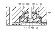
- 下部電極、誘電体、及び上部電極からなるキャパシタを有する半導体装置において、
前記上部電極の上面のみに接しスパッタ法により成膜された柱状構造をなす第1のAl2O3膜と、
前記上部電極の側面に接し前記第1のAl2O3膜の上側にスパッタ法により成膜された柱状構造をなす第2のAl2O3膜と、
前記第2のAl2O3膜の上側にCVD法により成膜された第3のAl2O3膜と、
前記キャパシタの上方における前記第1のAl 2 O 3 膜と前記第2のAl 2 O 3 膜の間に設けられた第1の膜と、
を備えたことを特徴とする半導体装置。 - 前記CVD法はALD法であることを特徴とする請求項1に記載の半導体装置。
- 前記第2のAl2O3膜は前記誘電体に接することを特徴とする請求項1または2に記載の半導体装置。
- 前記第2のAl 2 O 3 膜と前記第3のAl 2 O 3 膜との間に第2の膜を備え、前記キャパシタの側面において前記第2のAl2O3膜の側面部が前記第3のAl2O3膜に接していることを特徴とする請求項1乃至3のいずれかに記載の半導体装置。
- 下部電極、誘電体、及び上部電極からなるキャパシタを有する半導体装置の製造方法において、
前記上部電極の上面のみに接する第1のAl2O3膜をスパッタ法により成膜し、
前記キャパシタの上方における前記第1のAl 2 O 3 膜の上側に第1の膜を成膜し、
前記第1の膜の上側に前記上部電極の側面に接する第2のAl2O3膜をスパッタ法により成膜し、
前記第2のAl2O3膜の上側に第3のAl2O3膜をCVD法により成膜することを特徴とする半導体装置の製造方法。 - 前記CVD法はALD法であることを特徴とする請求項5に記載の半導体装置の製造方法。
- 前記第2のAl2O3膜は前記誘電体に接することを特徴とする請求項5または6に記載の半導体装置の製造方法。
- 前記第2のAl 2 O 3 膜と前記第3のAl 2 O 3 膜との間に第2の膜をさらに成膜し、前記キャパシタの側面において前記第2のAl2O3膜の側面部が前記第3のAl2O3膜に接していることを特徴とする請求項5乃至7のいずれかに記載の半導体装置の製造方法。
Priority Applications (2)
| Application Number | Priority Date | Filing Date | Title |
|---|---|---|---|
| JP2004143428A JP4105656B2 (ja) | 2004-05-13 | 2004-05-13 | 半導体装置及びその製造方法 |
| US10/856,868 US20050255663A1 (en) | 2004-05-13 | 2004-06-01 | Semiconductor device and method of manufacturing the same |
Applications Claiming Priority (1)
| Application Number | Priority Date | Filing Date | Title |
|---|---|---|---|
| JP2004143428A JP4105656B2 (ja) | 2004-05-13 | 2004-05-13 | 半導体装置及びその製造方法 |
Publications (2)
| Publication Number | Publication Date |
|---|---|
| JP2005327847A JP2005327847A (ja) | 2005-11-24 |
| JP4105656B2 true JP4105656B2 (ja) | 2008-06-25 |
Family
ID=35309956
Family Applications (1)
| Application Number | Title | Priority Date | Filing Date |
|---|---|---|---|
| JP2004143428A Expired - Fee Related JP4105656B2 (ja) | 2004-05-13 | 2004-05-13 | 半導体装置及びその製造方法 |
Country Status (2)
| Country | Link |
|---|---|
| US (1) | US20050255663A1 (ja) |
| JP (1) | JP4105656B2 (ja) |
Families Citing this family (11)
| Publication number | Priority date | Publication date | Assignee | Title |
|---|---|---|---|---|
| JP4284228B2 (ja) * | 2004-04-19 | 2009-06-24 | 株式会社東芝 | 半導体装置の製造方法 |
| JP2006005234A (ja) * | 2004-06-18 | 2006-01-05 | Seiko Epson Corp | 半導体装置の製造方法及び半導体装置 |
| CN100431155C (zh) * | 2004-06-28 | 2008-11-05 | 富士通株式会社 | 半导体器件及其制造方法 |
| JP4497312B2 (ja) * | 2004-10-19 | 2010-07-07 | セイコーエプソン株式会社 | 強誘電体メモリの製造方法 |
| JP4953580B2 (ja) * | 2005-03-03 | 2012-06-13 | 富士通セミコンダクター株式会社 | 半導体装置の製造方法 |
| JP2006310637A (ja) * | 2005-04-28 | 2006-11-09 | Toshiba Corp | 半導体装置 |
| KR101287201B1 (ko) * | 2005-12-30 | 2013-07-16 | 엘지디스플레이 주식회사 | 전기변색소자 및 이의 제조방법 |
| DE102010024079B4 (de) | 2010-06-17 | 2025-08-28 | OSRAM Opto Semiconductors Gesellschaft mit beschränkter Haftung | Verfahren zur Herstellung eines optoelektronischen Halbleiterchips und optoelektronischer Halbleiterchip |
| JP5672832B2 (ja) * | 2010-08-06 | 2015-02-18 | 富士通セミコンダクター株式会社 | 半導体装置とその製造方法 |
| JP2016012609A (ja) * | 2014-06-27 | 2016-01-21 | 東京エレクトロン株式会社 | エッチング方法 |
| US12453105B2 (en) * | 2021-08-26 | 2025-10-21 | Taiwan Semiconductor Manufacturing Company Limited | Memory chiplet having multiple arrays of memory devices and methods of forming the same |
Family Cites Families (17)
| Publication number | Priority date | Publication date | Assignee | Title |
|---|---|---|---|---|
| US6509601B1 (en) * | 1998-07-31 | 2003-01-21 | Samsung Electronics Co., Ltd. | Semiconductor memory device having capacitor protection layer and method for manufacturing the same |
| US6611014B1 (en) * | 1999-05-14 | 2003-08-26 | Kabushiki Kaisha Toshiba | Semiconductor device having ferroelectric capacitor and hydrogen barrier film and manufacturing method thereof |
| KR100323874B1 (ko) * | 1999-12-22 | 2002-02-16 | 박종섭 | 반도체 소자의 알루미늄 산화막 형성 방법 |
| US6534809B2 (en) * | 1999-12-22 | 2003-03-18 | Agilent Technologies, Inc. | Hardmask designs for dry etching FeRAM capacitor stacks |
| US6730951B2 (en) * | 2001-06-25 | 2004-05-04 | Matsushita Electric Industrial Co., Ltd. | Capacitor, semiconductor memory device, and method for manufacturing the same |
| KR100423906B1 (ko) * | 2001-08-08 | 2004-03-22 | 삼성전자주식회사 | 강유전성 메모리 장치 및 그 제조방법 |
| US20030143853A1 (en) * | 2002-01-31 | 2003-07-31 | Celii Francis G. | FeRAM capacitor stack etch |
| JP2004071932A (ja) * | 2002-08-08 | 2004-03-04 | Toshiba Corp | 半導体装置 |
| US6621683B1 (en) * | 2002-09-19 | 2003-09-16 | Infineon Technologies Aktiengesellschaft | Memory cells with improved reliability |
| US7091102B2 (en) * | 2002-12-20 | 2006-08-15 | Samsung Electronics Co., Ltd. | Methods of forming integrated circuit devices having a capacitor with a hydrogen barrier spacer on a sidewall thereof and integrated circuit devices formed thereby |
| KR100532427B1 (ko) * | 2003-03-27 | 2005-11-30 | 삼성전자주식회사 | 강유전체 메모리 소자의 제조 방법 |
| US20040206993A1 (en) * | 2003-04-17 | 2004-10-21 | Infineon Technologies Ag | Process for fabrication of ferroelectric devices with reduced hydrogen ion damage |
| US6839220B1 (en) * | 2003-07-18 | 2005-01-04 | Infineon Technologies Ag | Multi-layer barrier allowing recovery anneal for ferroelectric capacitors |
| US7101785B2 (en) * | 2003-07-22 | 2006-09-05 | Infineon Technologies Ag | Formation of a contact in a device, and the device including the contact |
| US7001781B2 (en) * | 2003-09-26 | 2006-02-21 | Infineon Technologies Ag | Method for producing a ferroelectric capacitor that includes etching with hardmasks |
| US7001821B2 (en) * | 2003-11-10 | 2006-02-21 | Texas Instruments Incorporated | Method of forming and using a hardmask for forming ferroelectric capacitors in a semiconductor device |
| JP4522088B2 (ja) * | 2003-12-22 | 2010-08-11 | 富士通セミコンダクター株式会社 | 半導体装置の製造方法 |
-
2004
- 2004-05-13 JP JP2004143428A patent/JP4105656B2/ja not_active Expired - Fee Related
- 2004-06-01 US US10/856,868 patent/US20050255663A1/en not_active Abandoned
Also Published As
| Publication number | Publication date |
|---|---|
| JP2005327847A (ja) | 2005-11-24 |
| US20050255663A1 (en) | 2005-11-17 |
Similar Documents
| Publication | Publication Date | Title |
|---|---|---|
| US8236643B2 (en) | Method of manufacturing semiconductor device including ferroelectric capacitor | |
| JP5251864B2 (ja) | 半導体装置及びその製造方法 | |
| JP2008198813A (ja) | 半導体装置及びその製造方法 | |
| JP4884104B2 (ja) | キャパシタを含む半導体装置及びその製造方法 | |
| US20060183250A1 (en) | Methods of fabricating ferroelectric capacitors utilizing a partial chemical mechanical polishing process | |
| JP2005327847A (ja) | 半導体装置及びその製造方法 | |
| KR101262432B1 (ko) | 반도체 장치의 제조 방법 | |
| US7573120B2 (en) | Semiconductor device and method of manufacturing the same | |
| WO2006134664A1 (ja) | 半導体装置及びその製造方法 | |
| US20040130026A1 (en) | Semiconductor device and method of manufacturing the same | |
| US20020151162A1 (en) | Method of producing a capacitor electrode with a barrier structure | |
| JP4284228B2 (ja) | 半導体装置の製造方法 | |
| JP5487140B2 (ja) | 半導体装置の製造方法 | |
| JP2010003741A (ja) | 半導体装置及び半導体装置の製造方法 | |
| JP4845624B2 (ja) | 半導体装置とその製造方法 | |
| JP4220459B2 (ja) | 半導体装置 | |
| KR100403957B1 (ko) | 강유전체 메모리 소자의 제조 방법 | |
| JP4095582B2 (ja) | 半導体装置及びその製造方法 | |
| JP2009105223A (ja) | 半導体装置及びその製造方法 | |
| JP2009105388A (ja) | 半導体装置及びその製造方法 | |
| JP2006269800A (ja) | 半導体装置 | |
| JP5326256B2 (ja) | 半導体装置の製造方法 | |
| JP5007723B2 (ja) | キャパシタを含む半導体装置及びその製造方法 | |
| JP2007266023A (ja) | 半導体装置、及び半導体装置の製造方法 | |
| JP2006134961A (ja) | 半導体装置 |
Legal Events
| Date | Code | Title | Description |
|---|---|---|---|
| A977 | Report on retrieval |
Free format text: JAPANESE INTERMEDIATE CODE: A971007 Effective date: 20060804 |
|
| A131 | Notification of reasons for refusal |
Free format text: JAPANESE INTERMEDIATE CODE: A131 Effective date: 20060808 |
|
| A521 | Request for written amendment filed |
Free format text: JAPANESE INTERMEDIATE CODE: A523 Effective date: 20061108 |
|
| A131 | Notification of reasons for refusal |
Free format text: JAPANESE INTERMEDIATE CODE: A131 Effective date: 20071211 |
|
| A521 | Request for written amendment filed |
Free format text: JAPANESE INTERMEDIATE CODE: A523 Effective date: 20080228 |
|
| TRDD | Decision of grant or rejection written | ||
| A01 | Written decision to grant a patent or to grant a registration (utility model) |
Free format text: JAPANESE INTERMEDIATE CODE: A01 Effective date: 20080325 |
|
| A61 | First payment of annual fees (during grant procedure) |
Free format text: JAPANESE INTERMEDIATE CODE: A61 Effective date: 20080327 |
|
| R150 | Certificate of patent or registration of utility model |
Free format text: JAPANESE INTERMEDIATE CODE: R150 |
|
| FPAY | Renewal fee payment (event date is renewal date of database) |
Free format text: PAYMENT UNTIL: 20110404 Year of fee payment: 3 |
|
| LAPS | Cancellation because of no payment of annual fees |