JP4133580B2 - Processing method of piezoelectric material - Google Patents
Processing method of piezoelectric material Download PDFInfo
- Publication number
- JP4133580B2 JP4133580B2 JP2003142894A JP2003142894A JP4133580B2 JP 4133580 B2 JP4133580 B2 JP 4133580B2 JP 2003142894 A JP2003142894 A JP 2003142894A JP 2003142894 A JP2003142894 A JP 2003142894A JP 4133580 B2 JP4133580 B2 JP 4133580B2
- Authority
- JP
- Japan
- Prior art keywords
- mask
- piezoelectric material
- substrate
- processed
- thickness distribution
- Prior art date
- Legal status (The legal status is an assumption and is not a legal conclusion. Google has not performed a legal analysis and makes no representation as to the accuracy of the status listed.)
- Expired - Fee Related
Links
Images
Classifications
-
- C—CHEMISTRY; METALLURGY
- C04—CEMENTS; CONCRETE; ARTIFICIAL STONE; CERAMICS; REFRACTORIES
- C04B—LIME, MAGNESIA; SLAG; CEMENTS; COMPOSITIONS THEREOF, e.g. MORTARS, CONCRETE OR LIKE BUILDING MATERIALS; ARTIFICIAL STONE; CERAMICS; REFRACTORIES; TREATMENT OF NATURAL STONE
- C04B41/00—After-treatment of mortars, concrete, artificial stone or ceramics; Treatment of natural stone
- C04B41/80—After-treatment of mortars, concrete, artificial stone or ceramics; Treatment of natural stone of only ceramics
- C04B41/91—After-treatment of mortars, concrete, artificial stone or ceramics; Treatment of natural stone of only ceramics involving the removal of part of the materials of the treated articles, e.g. etching
-
- H—ELECTRICITY
- H10—SEMICONDUCTOR DEVICES; ELECTRIC SOLID-STATE DEVICES NOT OTHERWISE PROVIDED FOR
- H10N—ELECTRIC SOLID-STATE DEVICES NOT OTHERWISE PROVIDED FOR
- H10N30/00—Piezoelectric or electrostrictive devices
- H10N30/01—Manufacture or treatment
- H10N30/08—Shaping or machining of piezoelectric or electrostrictive bodies
- H10N30/082—Shaping or machining of piezoelectric or electrostrictive bodies by etching, e.g. lithography
-
- H—ELECTRICITY
- H10—SEMICONDUCTOR DEVICES; ELECTRIC SOLID-STATE DEVICES NOT OTHERWISE PROVIDED FOR
- H10P—GENERIC PROCESSES OR APPARATUS FOR THE MANUFACTURE OR TREATMENT OF DEVICES COVERED BY CLASS H10
- H10P50/00—Etching of wafers, substrates or parts of devices
- H10P50/20—Dry etching; Plasma etching; Reactive-ion etching
- H10P50/24—Dry etching; Plasma etching; Reactive-ion etching of semiconductor materials
- H10P50/242—Dry etching; Plasma etching; Reactive-ion etching of semiconductor materials of Group IV materials
-
- H—ELECTRICITY
- H03—ELECTRONIC CIRCUITRY
- H03H—IMPEDANCE NETWORKS, e.g. RESONANT CIRCUITS; RESONATORS
- H03H3/00—Apparatus or processes specially adapted for the manufacture of impedance networks, resonating circuits, resonators
- H03H3/007—Apparatus or processes specially adapted for the manufacture of impedance networks, resonating circuits, resonators for the manufacture of electromechanical resonators or networks
- H03H3/02—Apparatus or processes specially adapted for the manufacture of impedance networks, resonating circuits, resonators for the manufacture of electromechanical resonators or networks for the manufacture of piezoelectric or electrostrictive resonators or networks
Landscapes
- Engineering & Computer Science (AREA)
- Manufacturing & Machinery (AREA)
- Chemical & Material Sciences (AREA)
- Ceramic Engineering (AREA)
- Materials Engineering (AREA)
- Structural Engineering (AREA)
- Organic Chemistry (AREA)
- Drying Of Semiconductors (AREA)
- Piezo-Electric Or Mechanical Vibrators, Or Delay Or Filter Circuits (AREA)
- Micromachines (AREA)
- Compositions Of Oxide Ceramics (AREA)
Description
【技術分野】
【0001】
本発明は、水晶,PZT(チタン酸ジルコン酸鉛),LiNbO3等の圧電材料を任意形状に加工し、超音波振動の制御,振動特性の改善を可能にした加工方法に関する。
【背景技術】
【0002】
圧電素子は基準周波数の発振源,電子電気機器用クロック等、広範な分野で使用されており、情報処理・伝達能力を高性能化するための薄型化や高品質化のためのレンズ形状への加工法に関する研究・開発が進められている。
電極直径が数mm以上の大型振動子では、湿式エッチング後で整形した凸部の端面を機械研磨等で曲面に加工する方法が採用されている。電極直径1mm以下の小型振動子では、凹面加工により支持損失を低減した高品質の振動子を製作している。凹面加工の一形態として、最終目標に近いプロフィールに成形した後でドライエッチングする方法も紹介されている(特許文献1)。
【特許文献1】
特開2002−368572号公報
【0003】
機械研磨では、定盤に取り付けた研磨布で圧電材料の表面を研磨しているが、圧電材料の結晶にダメージを与えやすい。また、研磨台に配置した小さな振動子全てを目標形状に仕上げることは不可能であり、形状の自由度も低い。凹面加工では、薄層化による高周波化,支持損失の低減による高いQ値を得やすいが、三次元形状への加工が困難なため振動子中央部に大きな質量を分布させ難い。その結果、質量負荷に対して振動が不安定になりやすい。
【発明の開示】
【発明が解決しようとする課題】
【0004】
本発明は、このような問題を解消すべく案出されたものであり、目標形状に対応する膜厚分布をもつマスクを圧電材料(被加工材)の表面に設けた後でドライエッチングすることにより、大面積への対応,超小型化,集積化,加工自由度の全てに優れ、高精度で三次元形状に加工された圧電材料を得ることをを目的とする。
【課題を解決するための手段】
【0005】
本発明に従った加工方法では、圧電材料に比較して加工速度が異なるマスク材料から成膜されたマスクを圧電材料の被加工面に設ける。パターニングされたマスク材料の加熱溶融等により、マスクに所定の膜厚分布を付与する。マスクの形成に先立って、加工速度比を増幅させる薄膜を圧電材料/マスクの界面に介在させても良い。
マスクが設けられた圧電材料をドライエッチングすると、マスクの膜厚分布に倣った形状に圧電材料が加工される。ドライエッチングの初期に選択反応性の低いガス組成を使用してマスク,圧電材料の表面層をエッチング除去した後、圧電材料に対する選択反応性の高いガス組成に切り替えると、マスクの膜厚分布が増幅された三次元形状に圧電材料が加工される。
すなわち、本発明によれば、圧電材料基板の表面にマスク材料の膜を形成した後、前記マスク材料の膜をパターニングした後、加熱溶融によりリフローさせることにより、前記マスク材料の膜にコンベックス形状に対応する膜厚分布を持たせ、この膜厚分布を持つマスク材料の膜および前記圧電材料基板をドライエッチングして、前記圧電材料基板の表面を、前記マスク材料の膜の膜厚分布を反映したコンベックス形状に加工することを特徴とする圧電材料基板の加工方法が提供される。
【発明の効果】
【0006】
ドライエッチングされた圧電材料は、マスクの膜厚分布を反映した三次元形状に加工される。圧電材料との関係でマスク材料を選択して圧電材料,マスクの加工速度比を調節し、或いは反応性の低いガス組成から圧電材料に対する選択反応性の高いガス組成に切り替えながらドライエッチングするとき、マスクの膜厚分布を増幅させた三次元形状にも加工できる。大面積の圧電材料であっても、複雑で任意の形状への加工が容易である。しかも、ドライエッチングによる加工であるため、結晶欠陥の原因となる歪みの導入や異物の混入がなく、面内方向の質量分布がニーズに応じて制御された高品質の圧電素子が得られる。
【0007】
振動エネルギーが質量に依存する特性を示す圧電素子では、予めニーズに対応した面内質量分布を適正化して電極を配置するとき、電気エネルギーから機械振動エネルギーへの効率的な変換が促進される。そのため、大きな負荷がかかる吸着物の測定,外界への振動の伝播等の目的に対応した優れた振動子を実現する上で、質量分布を三次元的に整形する加工技術が重要である。
【0008】
機械加工,レーザ加工によるとき加工自由度は高くなるが、大半の圧電材料は脆性材料であり、加工時の熱で結晶構造が変化する虞もある。そのため、高品位振動子の作製に適した加工法が要求される。この点、加工時に機械的,熱的な応力の導入がないドライエッチングによるとき、結晶構造に悪影響を与えることなく圧電材料を目標とする三次元形状に高精度加工できる。ドライエッチング法は、他の方法に比較して、小型化,大量一括生産にも適している。
【発明を実施するための最良の形態】
【0009】
コンベックス型水晶振動子マイクロバランスの加工を例にとって本発明を具体的に説明する。
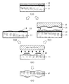
先ず、被加工基板11(圧電材料基板)に加工速度比増幅膜12を介しマスク13を形成する(図1A)。増幅膜12は、被加工基板11と加工速度が異なる無機質金属,セラミック等から成膜され、ドライエッチングによる被加工基板11,マスク13の加工速度比を調整するために必要に応じて設けられる。
【0010】
フォトレジストから成膜されるマスク13では、たとえば圧電材料基板11にフォトレジストを塗布した後、周縁部に照射される光量が中央部より少なくなる条件下でレジスト膜を露光し、現像することにより、厚膜の中央部から周縁部に向けて薄くなる膜厚分布をもつマスク14に整形できる。圧電材料(被加工基板11)に比較してフォトレジスト製マスク14のエッチング速度は一般的に低いので、通常条件下のドライエッチングで形成される凹凸が浅くなる。
【0011】
より立体的な形状の転写が要求される場合、錫,低融点ガラス,フリット等、低融点の無機質金属やセラミックスをリフローすることにより、被加工基板11に比較して加工速度が低いマスク14を形成する(図1B)。マスク14は、フォトレジスト製マスク13の上に積層しても良い。
【0012】
別な基板に予め形成した精密型15をマスク13に圧着し、膜厚分布が制御されたマスク14に整形する方法も採用できる(図1C)。精密型15を使用する場合、マスク13に対向する精密型15の作用面に剥離紙16を敷き、整形されたマスク14から精密型15の分離を容易にすることが好ましい。
リフロー,精密型15の圧着何れによる場合でも、厚い中央部から周縁部に向けて徐々に薄くなる膜厚分布をもつマスク14に整形される。
【0013】
膜厚分布が制御されたマスク14を設けた被加工基板11をドライエッチングすると、マスク14の膜厚分布が反映された形状(図1D)に被加工基板11の表面層が加工され、目標形状(図1E)をもつ圧電素子素材17が得られる。
被加工基板11に転写される三次元形状の凹凸は、被加工基板11とマスク14の加工速度比調節によっても制御される。たとえば、ドライエッチングでは、被加工基板11を選択的に加工又は脆弱化するラジカル等の供給源としてPFC(パーフルオロカーボン),SF6,塩素,ヨウ素系のガス(以下、選択反応性ガスという)と選択性のない物理的エッチング作用を呈するAr,Kr,Xe等のガス(以下、非選択性ガスという)が使用されるが、選択反応性ガスと非選択性ガスの比率を変えることにより加工速度比を制御できる。或いは、プラズマ発生の投入パワーによっても加工速度比が制御される。
【0014】
たとえば、整形されたフォトレジスト製マスク14をドライエッチングする途中で、非選択性ガスの多いガス組成から選択反応性ガスの多いガス組成に切り替える。非選択性ガスの比率が高いドライエッチングでは、マスク14の膜厚分布が被加工基板11に転写される。選択反応性ガスの比率が高いドライエッチングでは、被加工基板11が優先的にエッチングされる。その結果、マスク14の膜厚分布が増幅された三次元形状に被加工基板11を加工できる。
【実施例1】
【0015】
PZTを圧電材料基板11に使用し、ポジ型レジストをスピンコート法で塗布し、膜厚7μmのレジスト膜を形成した。濃淡のあるグレーティングマスクでフォトレジストを露光することにより膜厚分布が制御されたマスク14に整形した。整形されたマスク14は、断面が周期的なノコギリ歯形状になった膜厚分布をもっていた。
次いで、反応性ドライエッチングによりマスク14の膜厚分布を被加工基板11に転写した。SF6をエッチングガスに用いて10Pa以下の減圧雰囲気でドライエッチングしたところ、フォトレジスト,PZTの加工速度比は0.2程度であり、PZTの加工速度は0.1〜0.2μm/分であった。その結果、1μm程度の周期的なパターンをPZTに転写できた。
ドライエッチングされたPZTに電極をパターニングし、電圧を印加すると、基板上の微小物体を一定方向に運動させることができた。
【実施例2】
【0016】
圧電材料基板11に水晶を使用し、ポジ型レジストをスピンコート法で塗布し、膜厚4μmのレジスト膜を形成した。レジスト膜をパターニングしてコンベックス形状に整形した後、熱処理を施した。熱処理では、加熱温度を徐々に上げることによりレンズ形状にレジストをリフローさせることにより、膜厚分布が制御されたマスク14とした。
【0017】
次いで、反応性ドライエッチングによりマスク14の膜厚分布を被加工基板11に転写した。SF6,Xeの混合ガスをエッチングガスに用いて10Pa以下の減圧雰囲気でドライエッチングしたところ、フォトレジスト,水晶の加工速度比は0.3程度であり、水晶の加工速度は0.4〜0.6μm/分であった。その結果、マスク14のレンズ形状を倣った三次元形状に水晶を加工できた。
マスク14のレンズ高さを1.6μm程度にすると、振動特性が大幅に向上した圧電素子が得られ、未加工時に比較してQ値が2倍以上も高くなった。作製された圧電素子では、副振動も一桁近く低減されていた。
【実施例3】
【0018】
圧電材料基板11に水晶を使用し、ポジ型レジストをスピンコート法で塗布し、膜厚4μmのレジスト膜を形成した。レジスト膜をパターニングしてコンベックス形状に整形した後、熱処理を施した。熱処理では、加熱温度を徐々に上げることによりレンズ形状にレジストをリフローさせることにより、膜厚分布が制御されたマスク14とした。
【0019】
次いで、10Pa以下の減圧雰囲気で反応性ドライエッチングすることによりマスク14の膜厚分布を被加工基板11に転写した。エッチングガスには、SF6,Xeの混合ガスを用いた。エッチング初期に混合ガスの組成比をSF6:Xe=9:1として3分間エッチングすることにより、マスク14のコンベックスと水晶板との境界に高さ1μmの斜面を形成した。その後、ガス流量制御装置で数秒以内に組成比を1:1に変更したところ、加工速度比が0.4→0.2,水晶の加工速度が0.4μm/分→0.2μm/分以下と大幅に低下した。加工速度比,加工速度の低下に伴い、マスク14/水晶板の境界が緩やかな勾配をもつ斜面に整形された。
作製された圧電素子は、中央部に付与された曲面分布のため、共振周波数の鈍化が抑制された素子として使用できた。
【産業上の利用可能性】
【0020】
膜厚分布が制御されたマスク14を設けた圧電材料基板11をドライエッチングしているため、従来の湿式エッチング−機械研磨に比較して目標三次元形状に高精度で加工でき、中央部に大きな質量を分布させることも容易である。このように加工された圧電材料から作成される圧電素子は、質量負荷に対する振動が安定しているので、極微量のバイオ,化学物質を検出する分子認識センサ等を始めとして広範な分野で使用される。
【図面の簡単な説明】
【図1】 圧電材料を三次元加工する工程のフロー図
【符号の説明】
11:被加工基板(圧電材料) 12:加工速度比増幅膜 13:マスク
14:整形されたマスク 15:精密型 16:剥離紙 17:圧電素子素材(加工後)【Technical field】
[0001]
The present invention relates to a processing method in which a piezoelectric material such as quartz, PZT (lead zirconate titanate), LiNbO 3 or the like is processed into an arbitrary shape to enable control of ultrasonic vibration and improvement of vibration characteristics.
[Background]
[0002]
Piezoelectric elements are used in a wide range of fields such as oscillation sources for reference frequencies, clocks for electronic and electrical equipment, and so on to reduce the thickness and quality of lenses for higher information processing and transmission capabilities. Research and development on processing methods are underway.
For large vibrators having an electrode diameter of several millimeters or more, a method is employed in which the end face of the convex portion shaped after wet etching is processed into a curved surface by mechanical polishing or the like. For small vibrators with an electrode diameter of 1 mm or less, high-quality vibrators with reduced support loss are manufactured by concave processing. As one form of concave processing, a method of dry etching after forming a profile close to the final target has also been introduced (Patent Document 1).
[Patent Document 1]
Japanese Patent Laid-Open No. 2002-368572
In mechanical polishing, the surface of the piezoelectric material is polished with a polishing cloth attached to a surface plate, but the crystals of the piezoelectric material are easily damaged. Further, it is impossible to finish all the small vibrators arranged on the polishing table into a target shape, and the degree of freedom in shape is low. In the concave surface processing, it is easy to obtain a high Q value by increasing the frequency by reducing the thickness and reducing the support loss. As a result, vibration tends to become unstable with respect to the mass load.
DISCLOSURE OF THE INVENTION
[Problems to be solved by the invention]
[0004]
The present invention has been devised to solve such a problem, and a dry etching is performed after a mask having a film thickness distribution corresponding to a target shape is provided on the surface of a piezoelectric material (workpiece). Therefore, an object of the present invention is to obtain a piezoelectric material which is excellent in all areas, ultra-miniaturization, integration, and machining freedom, and is processed into a three-dimensional shape with high accuracy.
[Means for Solving the Problems]
[0005]
In the processing method according to the present invention, a mask formed from a mask material having a processing speed different from that of the piezoelectric material is provided on the processing surface of the piezoelectric material. By heating it dissolved Toruto the patterned mask material, to impart a predetermined film thickness distribution in the mask. Prior to formation of the mask, a thin film for amplifying the processing speed ratio may be interposed at the piezoelectric material / mask interface.
When the piezoelectric material provided with the mask is dry-etched, the piezoelectric material is processed into a shape that follows the film thickness distribution of the mask. When the mask and piezoelectric material surface layer is etched away using a gas composition with low selective reactivity at the beginning of dry etching, and then switched to a gas composition with high selective reactivity to the piezoelectric material, the mask thickness distribution is amplified. The piezoelectric material is processed into the three-dimensional shape.
That is, according to the present invention, after forming a film of a mask material on the surface of the piezoelectric material substrate, after patterning the film before Symbol mask material, by reflow by heat melting, convex shape in the membrane of the mask material The mask material film having the film thickness distribution and the piezoelectric material substrate are dry-etched to reflect the film thickness distribution of the mask material film on the surface of the piezoelectric material substrate. There is provided a method for processing a piezoelectric material substrate, characterized by processing into a convex shape.
【The invention's effect】
[0006]
The dry-etched piezoelectric material is processed into a three-dimensional shape that reflects the film thickness distribution of the mask. When performing dry etching while selecting the mask material in relation to the piezoelectric material and adjusting the processing speed ratio of the piezoelectric material and mask, or switching from a gas composition with low reactivity to a gas composition with high selectivity to the piezoelectric material, It can also be processed into a three-dimensional shape with an amplified mask thickness distribution. Even a piezoelectric material having a large area is complicated and can be easily processed into an arbitrary shape. In addition, since the processing is performed by dry etching, a high-quality piezoelectric element in which the mass distribution in the in-plane direction is controlled according to needs without the introduction of strain and the introduction of foreign matters that cause crystal defects can be obtained.
[0007]
In a piezoelectric element exhibiting a characteristic in which vibration energy depends on mass, efficient conversion from electrical energy to mechanical vibration energy is promoted when an in-plane mass distribution corresponding to needs is optimized and electrodes are arranged. Therefore, in order to realize an excellent vibrator corresponding to the purpose such as measurement of an adsorbate subject to a large load and propagation of vibration to the outside world, a processing technique for shaping the mass distribution three-dimensionally is important.
[0008]
When machining and laser processing are performed, the degree of freedom of processing is high, but most piezoelectric materials are brittle materials, and the crystal structure may change due to heat during processing. Therefore, a processing method suitable for manufacturing a high-quality vibrator is required. In this regard, when dry etching that does not introduce mechanical or thermal stress during processing is performed, the piezoelectric material can be processed with high precision into a target three-dimensional shape without adversely affecting the crystal structure. The dry etching method is suitable for downsizing and mass production as compared with other methods.
BEST MODE FOR CARRYING OUT THE INVENTION
[0009]
The present invention will be described in detail by taking an example of processing a convex-type crystal resonator microbalance.
First, a
[0010]
In the
[0011]
When more three-dimensional shape transfer is required, a
[0012]
It is also possible to employ a method in which a
In either case of reflow or pressure bonding of the
[0013]
When the processed
The three-dimensional unevenness transferred to the
[0014]
For example, during dry etching of the shaped
[Example 1]
[0015]
PZT was used for the
Next, the film thickness distribution of the
When the electrodes were patterned on the dry-etched PZT and a voltage was applied, a minute object on the substrate could be moved in a certain direction.
[Example 2]
[0016]
Quartz was used for the
[0017]
Next, the film thickness distribution of the
When the lens height of the
[Example 3]
[0018]
Quartz was used for the
[0019]
Next, the film thickness distribution of the
The produced piezoelectric element was able to be used as an element in which the resonance frequency was suppressed from slowing due to the curved surface distribution given to the central part.
[Industrial applicability]
[0020]
Since the
[Brief description of the drawings]
1] Flow diagram of the process of three-dimensional processing of piezoelectric material [Explanation of symbols]
11: Substrate to be processed (piezoelectric material) 12: Processing speed ratio amplification film 13: Mask 14: Shaped mask 15: Precision mold 16: Release paper 17: Piezoelectric element material (after processing)
Claims (1)
Priority Applications (6)
| Application Number | Priority Date | Filing Date | Title |
|---|---|---|---|
| JP2003142894A JP4133580B2 (en) | 2003-05-21 | 2003-05-21 | Processing method of piezoelectric material |
| US10/556,930 US20070000864A1 (en) | 2003-05-21 | 2004-05-20 | Piezoelectric material working method |
| CNA2004800135361A CN1791565A (en) | 2003-05-21 | 2004-05-20 | Processing methods of piezoelectric materials |
| EP04745353A EP1632466A4 (en) | 2003-05-21 | 2004-05-20 | PROCESS FOR MACHINING A PIEZOELECTRIC MATERIAL |
| KR20057021399A KR100847321B1 (en) | 2003-05-21 | 2004-05-20 | Piezoelectric material working method |
| PCT/JP2004/007220 WO2004103932A1 (en) | 2003-05-21 | 2004-05-20 | Piezoelectric material working method |
Applications Claiming Priority (1)
| Application Number | Priority Date | Filing Date | Title |
|---|---|---|---|
| JP2003142894A JP4133580B2 (en) | 2003-05-21 | 2003-05-21 | Processing method of piezoelectric material |
Publications (2)
| Publication Number | Publication Date |
|---|---|
| JP2004349365A JP2004349365A (en) | 2004-12-09 |
| JP4133580B2 true JP4133580B2 (en) | 2008-08-13 |
Family
ID=33475102
Family Applications (1)
| Application Number | Title | Priority Date | Filing Date |
|---|---|---|---|
| JP2003142894A Expired - Fee Related JP4133580B2 (en) | 2003-05-21 | 2003-05-21 | Processing method of piezoelectric material |
Country Status (6)
| Country | Link |
|---|---|
| US (1) | US20070000864A1 (en) |
| EP (1) | EP1632466A4 (en) |
| JP (1) | JP4133580B2 (en) |
| KR (1) | KR100847321B1 (en) |
| CN (1) | CN1791565A (en) |
| WO (1) | WO2004103932A1 (en) |
Cited By (1)
| Publication number | Priority date | Publication date | Assignee | Title |
|---|---|---|---|---|
| JPH0585571U (en) * | 1992-04-23 | 1993-11-19 | リョービ株式会社 | Nose part of impact tool |
Families Citing this family (12)
| Publication number | Priority date | Publication date | Assignee | Title |
|---|---|---|---|---|
| JP4012156B2 (en) | 2004-02-02 | 2007-11-21 | 独立行政法人科学技術振興機構 | Method for manufacturing piezoelectric element |
| US7955516B2 (en) | 2006-11-02 | 2011-06-07 | Applied Materials, Inc. | Etching of nano-imprint templates using an etch reactor |
| JP2008270416A (en) * | 2007-04-18 | 2008-11-06 | Sanken Electric Co Ltd | Method for forming a rough surface on an object |
| CN103026520B (en) * | 2010-07-26 | 2015-06-17 | 富士胶片株式会社 | Device having a curved piezoelectric membrane |
| WO2012112540A2 (en) | 2011-02-15 | 2012-08-23 | Fujifilm Dimatix, Inc. | Piezoelectric transducers using micro-dome arrays |
| FR2988911A1 (en) * | 2012-04-02 | 2013-10-04 | St Microelectronics Crolles 2 | CURVED PLATE AND METHOD OF MANUFACTURE |
| FR2988912A1 (en) | 2012-04-02 | 2013-10-04 | St Microelectronics Crolles 2 | ENERGY RECOVERY DEVICE |
| KR20150013508A (en) * | 2012-04-26 | 2015-02-05 | 도레이 카부시키가이샤 | Method for manufacturing crystal substrate having uneven structure |
| JP7029640B2 (en) * | 2018-07-03 | 2022-03-04 | パナソニックIpマネジメント株式会社 | Method of processing plate materials and method of manufacturing element chips |
| JP7146499B2 (en) * | 2018-07-17 | 2022-10-04 | 東京計器株式会社 | Method for manufacturing three-dimensional structural member, method for manufacturing acceleration pickup member, acceleration pickup member, and acceleration sensor |
| JP7456264B2 (en) * | 2020-04-24 | 2024-03-27 | セイコーエプソン株式会社 | Vibration element manufacturing method, vibration element and vibrator |
| CN111875378A (en) * | 2020-07-14 | 2020-11-03 | 中国船舶重工集团公司第七一五研究所 | PZT-based high Curie temperature piezoelectric ceramic and preparation method thereof |
Family Cites Families (13)
| Publication number | Priority date | Publication date | Assignee | Title |
|---|---|---|---|---|
| JP2795126B2 (en) * | 1993-04-16 | 1998-09-10 | 株式会社デンソー | Curved surface processing method and device |
| US6562523B1 (en) * | 1996-10-31 | 2003-05-13 | Canyon Materials, Inc. | Direct write all-glass photomask blanks |
| US5920786A (en) * | 1998-04-15 | 1999-07-06 | Advanced Micro Devices | Method for fabricating shallow isolation trenches using angular photoresist profiles to create sloped isolation trench walls |
| JP3731348B2 (en) * | 1998-06-09 | 2006-01-05 | 松下電器産業株式会社 | Piezoelectric vibrator |
| JP2000232095A (en) * | 1999-02-12 | 2000-08-22 | Nippon Telegr & Teleph Corp <Ntt> | Method for forming fine pattern on semiconductor surface |
| JP2001111129A (en) * | 1999-10-09 | 2001-04-20 | Yoshiaki Nagaura | Piezoelectric element and working method therefor |
| US6420202B1 (en) * | 2000-05-16 | 2002-07-16 | Agere Systems Guardian Corp. | Method for shaping thin film resonators to shape acoustic modes therein |
| JP2002368572A (en) * | 2001-06-05 | 2002-12-20 | Yoshiaki Nagaura | Piezoelectric element or electronic material, acoustic-electric converter, and method of manufacturing the same |
| JP2002048907A (en) * | 2000-08-01 | 2002-02-15 | Canon Inc | Manufacturing method of diffractive optical element |
| JP2002090980A (en) * | 2000-09-20 | 2002-03-27 | Ricoh Opt Ind Co Ltd | Distributed density mask and method for producing the same |
| JP2003060481A (en) * | 2001-08-16 | 2003-02-28 | Citizen Watch Co Ltd | Piezoelectric oscillation element and manufacturing method therefor, and piezoelectric device |
| JP4968999B2 (en) * | 2001-09-17 | 2012-07-04 | リコー光学株式会社 | Manufacturing method of three-dimensional structure |
| US6849558B2 (en) * | 2002-05-22 | 2005-02-01 | The Board Of Trustees Of The Leland Stanford Junior University | Replication and transfer of microstructures and nanostructures |
-
2003
- 2003-05-21 JP JP2003142894A patent/JP4133580B2/en not_active Expired - Fee Related
-
2004
- 2004-05-20 KR KR20057021399A patent/KR100847321B1/en not_active Expired - Fee Related
- 2004-05-20 WO PCT/JP2004/007220 patent/WO2004103932A1/en not_active Ceased
- 2004-05-20 CN CNA2004800135361A patent/CN1791565A/en active Pending
- 2004-05-20 US US10/556,930 patent/US20070000864A1/en not_active Abandoned
- 2004-05-20 EP EP04745353A patent/EP1632466A4/en not_active Withdrawn
Cited By (1)
| Publication number | Priority date | Publication date | Assignee | Title |
|---|---|---|---|---|
| JPH0585571U (en) * | 1992-04-23 | 1993-11-19 | リョービ株式会社 | Nose part of impact tool |
Also Published As
| Publication number | Publication date |
|---|---|
| WO2004103932A1 (en) | 2004-12-02 |
| EP1632466A4 (en) | 2009-06-17 |
| EP1632466A1 (en) | 2006-03-08 |
| CN1791565A (en) | 2006-06-21 |
| JP2004349365A (en) | 2004-12-09 |
| US20070000864A1 (en) | 2007-01-04 |
| KR100847321B1 (en) | 2008-07-21 |
| KR20060028386A (en) | 2006-03-29 |
Similar Documents
| Publication | Publication Date | Title |
|---|---|---|
| JP4133580B2 (en) | Processing method of piezoelectric material | |
| KR102388994B1 (en) | Combined laser treatment of a solid body to be split | |
| CN116160121B (en) | A method for fabricating quartz vibrating beams based on frequency-doubled Bessel laser selective etching. | |
| TW520341B (en) | A method for manufacturing a chamber of the thin film bulk acoustic wave resonator (FBAR) | |
| JP4334864B2 (en) | Thin plate crystal wafer and method for manufacturing crystal resonator | |
| JP5182379B2 (en) | Manufacturing method of composite substrate | |
| JPH0963912A (en) | Manufacture of joined substrate | |
| JP2010183138A (en) | Method of manufacturing tuning fork crystal oscillator | |
| JP2008205888A (en) | Method for manufacturing piezoelectric vibrating piece and piezoelectric vibrating element | |
| JP2001274128A (en) | Polishing method of thin plate and method of manufacturing piezoelectric vibrating reed | |
| CN202931261U (en) | Composite substrate for elastic wave apparatus | |
| JP2005217370A (en) | Method for manufacturing piezoelectric element | |
| JPH11163654A (en) | Method of manufacturing reinforced piezoelectric substrate | |
| JP2000003845A (en) | Method of manufacturing mask for X-ray exposure | |
| JPH0680429A (en) | Glass optical element molder | |
| JP2008022378A (en) | Quartz vibrating piece and manufacturing method thereof | |
| JP4031171B2 (en) | Through hole formation method | |
| JPH0738363A (en) | Processing method of electronic parts | |
| CN108292699A (en) | Method for manufacturing mixed structure | |
| CN121573675B (en) | Method and device for efficiently stripping diamond by ultra-surface micro lens array | |
| CN119584840B (en) | A processing method for quartz devices and quartz devices. | |
| JP2020057851A (en) | Composite substrate for surface acoustic wave device and method of manufacturing the same | |
| JP2004032572A (en) | Manufacturing method of piezoelectric vibrator | |
| JP2011140117A (en) | Thin film actuator and inkjet head | |
| JP2010183137A (en) | Crystal vibration piece and method of manufacturing the same, vibrator, oscillator, and electronic equipment |
Legal Events
| Date | Code | Title | Description |
|---|---|---|---|
| A131 | Notification of reasons for refusal |
Free format text: JAPANESE INTERMEDIATE CODE: A131 Effective date: 20070206 |
|
| A521 | Request for written amendment filed |
Free format text: JAPANESE INTERMEDIATE CODE: A523 Effective date: 20070330 |
|
| RD03 | Notification of appointment of power of attorney |
Free format text: JAPANESE INTERMEDIATE CODE: A7423 Effective date: 20070330 |
|
| A02 | Decision of refusal |
Free format text: JAPANESE INTERMEDIATE CODE: A02 Effective date: 20070904 |
|
| A521 | Request for written amendment filed |
Free format text: JAPANESE INTERMEDIATE CODE: A523 Effective date: 20071026 |
|
| A911 | Transfer to examiner for re-examination before appeal (zenchi) |
Free format text: JAPANESE INTERMEDIATE CODE: A911 Effective date: 20071122 |
|
| A131 | Notification of reasons for refusal |
Free format text: JAPANESE INTERMEDIATE CODE: A131 Effective date: 20080219 |
|
| A521 | Request for written amendment filed |
Free format text: JAPANESE INTERMEDIATE CODE: A523 Effective date: 20080305 |
|
| TRDD | Decision of grant or rejection written | ||
| A01 | Written decision to grant a patent or to grant a registration (utility model) |
Free format text: JAPANESE INTERMEDIATE CODE: A01 Effective date: 20080507 |
|
| A01 | Written decision to grant a patent or to grant a registration (utility model) |
Free format text: JAPANESE INTERMEDIATE CODE: A01 |
|
| A61 | First payment of annual fees (during grant procedure) |
Free format text: JAPANESE INTERMEDIATE CODE: A61 Effective date: 20080602 |
|
| FPAY | Renewal fee payment (event date is renewal date of database) |
Free format text: PAYMENT UNTIL: 20110606 Year of fee payment: 3 |
|
| R150 | Certificate of patent or registration of utility model |
Free format text: JAPANESE INTERMEDIATE CODE: R150 |
|
| FPAY | Renewal fee payment (event date is renewal date of database) |
Free format text: PAYMENT UNTIL: 20120606 Year of fee payment: 4 |
|
| FPAY | Renewal fee payment (event date is renewal date of database) |
Free format text: PAYMENT UNTIL: 20130606 Year of fee payment: 5 |
|
| LAPS | Cancellation because of no payment of annual fees |