JP4137065B2 - 半導体装置、デバイス形成基板、配線接続試験方法、および半導体装置の製造方法 - Google Patents
半導体装置、デバイス形成基板、配線接続試験方法、および半導体装置の製造方法 Download PDFInfo
- Publication number
- JP4137065B2 JP4137065B2 JP2005033549A JP2005033549A JP4137065B2 JP 4137065 B2 JP4137065 B2 JP 4137065B2 JP 2005033549 A JP2005033549 A JP 2005033549A JP 2005033549 A JP2005033549 A JP 2005033549A JP 4137065 B2 JP4137065 B2 JP 4137065B2
- Authority
- JP
- Japan
- Prior art keywords
- wiring
- pattern
- substrate
- connection test
- semiconductor device
- Prior art date
- Legal status (The legal status is an assumption and is not a legal conclusion. Google has not performed a legal analysis and makes no representation as to the accuracy of the status listed.)
- Expired - Fee Related
Links
Images


Classifications
-
- H—ELECTRICITY
- H10—SEMICONDUCTOR DEVICES; ELECTRIC SOLID-STATE DEVICES NOT OTHERWISE PROVIDED FOR
- H10P—GENERIC PROCESSES OR APPARATUS FOR THE MANUFACTURE OR TREATMENT OF DEVICES COVERED BY CLASS H10
- H10P74/00—Testing or measuring during manufacture or treatment of wafers, substrates or devices
- H10P74/27—Structural arrangements therefor
- H10P74/277—Circuits for electrically characterising or monitoring manufacturing processes, e.g. circuits in tested chips or circuits in testing wafers
Landscapes
- Testing Or Measuring Of Semiconductors Or The Like (AREA)
- Internal Circuitry In Semiconductor Integrated Circuit Devices (AREA)
- Semiconductor Integrated Circuits (AREA)
- Analysing Materials By The Use Of Radiation (AREA)
- Testing Of Short-Circuits, Discontinuities, Leakage, Or Incorrect Line Connections (AREA)
- Tests Of Electronic Circuits (AREA)
Description
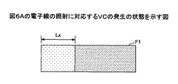
前記基板上に形成された絶縁層と、前記絶縁層に、互いに平行になるように形成された、前記電子線照射領域を有する複数の第1のパターン配線と、前記第1のパターン配線の間に形成され、前記第1のパターン配線よりも短い複数の第2のパターン配線と、前記第2のパターン配線の下層に形成された、前記第2のパターン配線に接続される第3のパターン配線と、前記第3のパターン配線の上層に形成された、当該第3のパターン配線と接続され、前記電子線照射領域を有する第4のパターン配線と、を有し、前記第1のパターン配線に電子線を放射して二次電子の放出を調べる第1の工程と、前記第4のパターン配線に電子線を放射して二次電子の放出を調べる第2の工程と、を有することを特徴とする配線接続試験方法により、解決する。
前記基板上に形成された半導体デバイスと、
前記基板上に形成された、電子線が照射されることで配線接続の試験を行う、電子線照射領域を含む配線接続試験構造と、を有する半導体装置であって、
前記配線接続試験構造は、
前記基板上に形成された絶縁層と、
前記絶縁層に、互いに平行になるように形成された、前記電子線照射領域を有する複数の第1のパターン配線と、
前記第1のパターン配線の間に形成された第2のパターン配線と、
前記第2のパターン配線の下層に形成された、前記第2のパターン配線に接続される第3のパターン配線と、
前記第3のパターン配線の上層に形成された、当該第3のパターン配線と接続され、前記電子線照射領域を有する第4のパターン配線と、を有することを特徴とする半導体装置。
前記基板上に形成された半導体デバイスと、
前記基板上に形成された、電子線が照射されることで配線接続の試験を行う、電子線照射領域を含む配線接続試験構造と、を有するデバイス形成基板であって、
前記配線接続試験構造は、
前記基板上に形成された絶縁層と、
前記絶縁層に、互いに平行になるように形成された、前記電子線照射領域を有する複数の第1のパターン配線と、
前記第1のパターン配線の間に形成された第2のパターン配線と、
前記第2のパターン配線の下層に形成された、前記第2のパターン配線に接続される第3のパターン配線と、
前記第3のパターン配線の上層に形成された、当該第3のパターン配線と接続され、前記電子線照射領域を有する第4のパターン配線と、を有することを特徴とするデバイス形成基板。
前記配線接続試験構造は、
前記基板上に形成された絶縁層と、
前記絶縁層に、互いに平行になるように形成された、前記電子線照射領域を有する複数の第1のパターン配線と、
前記第1のパターン配線の間に形成された第2のパターン配線と、
前記第2のパターン配線の下層に形成された、前記第2のパターン配線に接続される第3のパターン配線と、
前記第3のパターン配線の上層に形成された、当該第3のパターン配線と接続され、前記電子線照射領域を有する第4のパターン配線と、を有し、
前記第1のパターン配線に電子線を放射して二次電子の放出を調べる第1の工程と、
前記第4のパターン配線に電子線を放射して二次電子の放出を調べる第2の工程と、を有することを特徴とする配線接続試験方法。
前記基板上に半導体デバイスを形成する工程と、
前記基板上に前記配線接続試験構造を形成する工程と、
前記配線接続試験方法により、配線接続試験を実施する工程と、
前記配線接続試験の結果に対応して、前記半導体デバイスを形成する工程を制御するフィードバック工程と、を有することを特徴とする半導体装置の製造方法。
100A 半導体装置
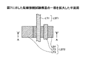
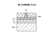
2,3,11,12,L1,L2,L3,L0,LT1,LT2,LT3,LB1,lt,lb,lt1,lt2,lt3,lb1,107,109 配線パターン
bp1,bp2,bp3,108 ビアプラグ
D1,D2,d1,d2,d3 絶縁層
ST1,ST2,LST1,LST2 配線構造
Sub,Sub1,Sub2 基板
105 素子分離絶縁膜
104a ソース領域
105b ドレイン領域
101 ゲート絶縁膜
102 ゲート電極
106 コンタクトプラグ
Claims (9)
- 基板と、
前記基板上に形成された半導体デバイスと、
前記基板上に形成された、電子線が照射されることで配線接続の試験を行う、電子線照射領域を含む配線接続試験構造と、を有する半導体装置であって、
前記配線接続試験構造は、
前記基板上に形成された絶縁層と、
前記絶縁層に、互いに平行になるように形成された、前記電子線照射領域を有する複数の第1のパターン配線と、
前記第1のパターン配線の間に形成され、前記第1のパターン配線よりも短い複数の第2のパターン配線と、
前記第2のパターン配線の下層に形成された、前記第2のパターン配線に接続される第3のパターン配線と、
前記第3のパターン配線の上層に形成された、当該第3のパターン配線と接続され、前記電子線照射領域を有する第4のパターン配線と、を有することを特徴とする半導体装置。 - 前記第3のパターン配線は、前記第1のパターン配線と直交する方向に形成されることを特徴とする請求項1記載の半導体装置。
- 前記複数の第2のパターン配線に対応して、それぞれ、複数の前記第3のパターン配線、および複数の前記第4のパターン配線がそれぞれ形成されていることを特徴とする請求項1または2記載の半導体装置。
- 前記第3のパターン配線には、複数の前記第2のパターン配線が接続されることを特徴とする請求項1乃至3のうち、いずれか1項記載の半導体装置。
- 前記第1のパターン配線と、互いに接続される前記第2のパターン配線と前記第3のパターン配線が、それぞれ前記基板に容量結合していることを特徴とする請求項1乃至4のうち、いずれか1項記載の半導体装置。
- 前記絶縁層は、多孔質材料よりなることを特徴とする請求項1乃至5のうち、いずれか1項記載の半導体装置。
- 基板と、
前記基板上に形成された半導体デバイスと、
前記基板上に形成された、電子線が照射されることで配線接続の試験を行う、電子線照射領域を含む配線接続試験構造と、を有するデバイス形成基板であって、
前記配線接続試験構造は、
前記基板上に形成された絶縁層と、
前記絶縁層に、互いに平行になるように形成された、前記電子線照射領域を有する複数の第1のパターン配線と、
前記第1のパターン配線の間に形成され、前記第1のパターン配線よりも短い複数の第2のパターン配線と、
前記第2のパターン配線の下層に形成された、前記第2のパターン配線に接続される第3のパターン配線と、
前記第3のパターン配線の上層に形成された、当該第3のパターン配線と接続され、前記電子線照射領域を有する第4のパターン配線と、を有することを特徴とするデバイス形成基板。 - 基板上に形成された、電子線照射領域を含む配線接続試験構造を用いた配線接続試験方法であって、
前記配線接続試験構造は、
前記基板上に形成された絶縁層と、
前記絶縁層に、互いに平行になるように形成された、前記電子線照射領域を有する複数の第1のパターン配線と、
前記第1のパターン配線の間に形成され、前記第1のパターン配線よりも短い複数の第2のパターン配線と、
前記第2のパターン配線の下層に形成された、前記第2のパターン配線に接続される第3のパターン配線と、
前記第3のパターン配線の上層に形成された、当該第3のパターン配線と接続され、前記電子線照射領域を有する第4のパターン配線と、を有し、
前記第1のパターン配線に電子線を放射して二次電子の放出を調べる第1の工程と、
前記第4のパターン配線に電子線を放射して二次電子の放出を調べる第2の工程と、を有することを特徴とする配線接続試験方法。 - 請求項8記載の配線接続試験方法を用いた半導体装置の製造方法であって、
前記基板上に半導体デバイスを形成する工程と、
前記基板上に前記配線接続試験構造を形成する工程と、
前記配線接続試験方法により、配線接続試験を実施する工程と、
前記配線接続試験の結果に対応して、前記半導体デバイスを形成する工程を制御するフィードバック工程と、を有することを特徴とする半導体装置の製造方法。
Priority Applications (4)
| Application Number | Priority Date | Filing Date | Title |
|---|---|---|---|
| JP2005033549A JP4137065B2 (ja) | 2005-02-09 | 2005-02-09 | 半導体装置、デバイス形成基板、配線接続試験方法、および半導体装置の製造方法 |
| TW094113240A TWI280388B (en) | 2005-02-09 | 2005-04-26 | Semiconductor device, device forming substrate, wiring connection testing method, and manufacturing method of the semiconductor device |
| US11/115,411 US7592623B2 (en) | 2005-02-09 | 2005-04-27 | Semiconductor device including wiring connection testing structure |
| CNB2005100727977A CN100465649C (zh) | 2005-02-09 | 2005-05-20 | 半导体器件及制造方法、器件形成基片和布线连接测试法 |
Applications Claiming Priority (1)
| Application Number | Priority Date | Filing Date | Title |
|---|---|---|---|
| JP2005033549A JP4137065B2 (ja) | 2005-02-09 | 2005-02-09 | 半導体装置、デバイス形成基板、配線接続試験方法、および半導体装置の製造方法 |
Publications (2)
| Publication Number | Publication Date |
|---|---|
| JP2006222233A JP2006222233A (ja) | 2006-08-24 |
| JP4137065B2 true JP4137065B2 (ja) | 2008-08-20 |
Family
ID=36779069
Family Applications (1)
| Application Number | Title | Priority Date | Filing Date |
|---|---|---|---|
| JP2005033549A Expired - Fee Related JP4137065B2 (ja) | 2005-02-09 | 2005-02-09 | 半導体装置、デバイス形成基板、配線接続試験方法、および半導体装置の製造方法 |
Country Status (4)
| Country | Link |
|---|---|
| US (1) | US7592623B2 (ja) |
| JP (1) | JP4137065B2 (ja) |
| CN (1) | CN100465649C (ja) |
| TW (1) | TWI280388B (ja) |
Families Citing this family (5)
| Publication number | Priority date | Publication date | Assignee | Title |
|---|---|---|---|---|
| US20070197020A1 (en) * | 2006-02-17 | 2007-08-23 | Texas Instruments Inc. | Inline method to detect and evaluate early failure rates of interconnects |
| JP5887760B2 (ja) * | 2011-08-24 | 2016-03-16 | 富士通株式会社 | 半導体装置の検査方法及び半導体装置の製造方法 |
| US9121884B2 (en) * | 2013-06-07 | 2015-09-01 | Infineon Technologies Ag | Capacitive test method, apparatus and system for semiconductor packages |
| JP6421463B2 (ja) * | 2014-06-02 | 2018-11-14 | 日本電産リード株式会社 | 基板検査装置、及び基板検査方法 |
| US11721576B2 (en) * | 2021-01-22 | 2023-08-08 | Taiwan Semiconductor Manufacturing Company Ltd. | Semiconductor devices and methods of manufacturing thereof |
Family Cites Families (13)
| Publication number | Priority date | Publication date | Assignee | Title |
|---|---|---|---|---|
| EP0622981B1 (en) * | 1993-04-27 | 1997-07-09 | Hitachi Chemical Co., Ltd. | Wiring board for electrical tests and method of manufacturing the same |
| JP2956830B2 (ja) * | 1996-11-21 | 1999-10-04 | 日本電気株式会社 | 半導体装置の製造方法 |
| US6307162B1 (en) * | 1996-12-09 | 2001-10-23 | International Business Machines Corporation | Integrated circuit wiring |
| JPH11242974A (ja) * | 1998-02-25 | 1999-09-07 | Sony Corp | 半導体装置用測定ソケット |
| US6636064B1 (en) * | 1999-12-14 | 2003-10-21 | Kla-Tencor | Dual probe test structures for semiconductor integrated circuits |
| WO2001063660A1 (en) * | 2000-02-25 | 2001-08-30 | Hitachi, Ltd. | Apparatus for detecting defect in device and method of detecting defect |
| WO2001080304A2 (en) | 2000-04-18 | 2001-10-25 | Kla-Tencor Corporation | Improved test structures and methods for inspecting and utilizing the same |
| JP2001305194A (ja) | 2000-04-27 | 2001-10-31 | Nec Corp | 半導体装置およびそのショート欠陥箇所の検出方法 |
| JP2003100097A (ja) * | 2001-09-25 | 2003-04-04 | Mitsubishi Electric Corp | 半導体記憶装置及びそのテスト方法 |
| US6771077B2 (en) * | 2002-04-19 | 2004-08-03 | Hitachi, Ltd. | Method of testing electronic devices indicating short-circuit |
| JP3776068B2 (ja) | 2002-09-02 | 2006-05-17 | 松下電器産業株式会社 | 半導体装置及びその検査方法 |
| JP3984521B2 (ja) * | 2002-09-20 | 2007-10-03 | 松下電器産業株式会社 | 透過型電子顕微鏡による観察方法 |
| US6822472B1 (en) * | 2003-06-27 | 2004-11-23 | International Business Machines Corporation | Detection of hard mask remaining on a surface of an insulating layer |
-
2005
- 2005-02-09 JP JP2005033549A patent/JP4137065B2/ja not_active Expired - Fee Related
- 2005-04-26 TW TW094113240A patent/TWI280388B/zh not_active IP Right Cessation
- 2005-04-27 US US11/115,411 patent/US7592623B2/en not_active Expired - Fee Related
- 2005-05-20 CN CNB2005100727977A patent/CN100465649C/zh not_active Expired - Fee Related
Also Published As
| Publication number | Publication date |
|---|---|
| CN1818669A (zh) | 2006-08-16 |
| TW200628816A (en) | 2006-08-16 |
| CN100465649C (zh) | 2009-03-04 |
| US20060175607A1 (en) | 2006-08-10 |
| JP2006222233A (ja) | 2006-08-24 |
| US7592623B2 (en) | 2009-09-22 |
| TWI280388B (en) | 2007-05-01 |
Similar Documents
| Publication | Publication Date | Title |
|---|---|---|
| TWI526697B (zh) | 用於檢測由自對準雙圖案製程製造的字元線陣列中缺陷的結構與方法 | |
| KR101333760B1 (ko) | 반도체 웨이퍼의 전자빔 검사용 반도체 집적 테스트 구조 | |
| US6855568B2 (en) | Apparatus and methods for monitoring self-aligned contact arrays using voltage contrast inspection | |
| TWI433160B (zh) | 積體電路製程中判定缺陷的結構與方法 | |
| TWI754151B (zh) | 晶圓級測試方法及其測試結構 | |
| CN112289795B (zh) | 三维存储器的漏电分析方法及三维存储器 | |
| US6204075B1 (en) | Method of detecting defects in a wiring process | |
| US9251581B1 (en) | Methods for promoting semiconductor manufacturing yield and classifying defects during fabricating a semiconductor device, and computer readable mediums encoded with a computer program implementing the same | |
| JP4137065B2 (ja) | 半導体装置、デバイス形成基板、配線接続試験方法、および半導体装置の製造方法 | |
| US20090212794A1 (en) | Test key for semiconductor structure | |
| CN102420015B (zh) | 用于一记忆体阵列中制造缺陷的检测的方法及测试装置 | |
| JP2001305194A (ja) | 半導体装置およびそのショート欠陥箇所の検出方法 | |
| US6858450B1 (en) | Method of alternating grounded/floating poly lines to monitor shorts | |
| US6545491B2 (en) | Apparatus for detecting defects in semiconductor devices and methods of using the same | |
| US9779910B1 (en) | Utilization of voltage contrast during sample preparation for transmission electron microscopy | |
| CN111668191B (zh) | 半导体结构及其制造方法与检测短路方法 | |
| JP2007019342A (ja) | 半導体装置のパイピング不良検出用teg並びにそのパイピング不良検出方法およびそのボイド形成状態判定方法 | |
| CN110879344A (zh) | 共享接触孔及其刻蚀缺陷检测方法 | |
| JP2008020251A (ja) | 欠陥検査方法、欠陥検査装置、及びパターン抽出方法 | |
| KR102670531B1 (ko) | 반도체 웨이퍼 검사 방법 및 시스템, 및 이를 이용한 반도체 소자의 제조 방법 | |
| US20160266191A1 (en) | Inspection apparatus and inspection method | |
| US6774648B1 (en) | Apparatus and methods for optically detecting defects in voltage contrast test structures | |
| JP2008311439A (ja) | 半導体装置およびその導体配線の接続検査方法 | |
| JP2007299904A (ja) | 半導体装置及びその検査方法 | |
| JP2007299904A5 (ja) |
Legal Events
| Date | Code | Title | Description |
|---|---|---|---|
| A977 | Report on retrieval |
Free format text: JAPANESE INTERMEDIATE CODE: A971007 Effective date: 20080121 |
|
| A131 | Notification of reasons for refusal |
Free format text: JAPANESE INTERMEDIATE CODE: A131 Effective date: 20080205 |
|
| A521 | Request for written amendment filed |
Free format text: JAPANESE INTERMEDIATE CODE: A523 Effective date: 20080404 |
|
| TRDD | Decision of grant or rejection written | ||
| A01 | Written decision to grant a patent or to grant a registration (utility model) |
Free format text: JAPANESE INTERMEDIATE CODE: A01 Effective date: 20080513 |
|
| A01 | Written decision to grant a patent or to grant a registration (utility model) |
Free format text: JAPANESE INTERMEDIATE CODE: A01 |
|
| A61 | First payment of annual fees (during grant procedure) |
Free format text: JAPANESE INTERMEDIATE CODE: A61 Effective date: 20080603 |
|
| R150 | Certificate of patent or registration of utility model |
Free format text: JAPANESE INTERMEDIATE CODE: R150 |
|
| FPAY | Renewal fee payment (event date is renewal date of database) |
Free format text: PAYMENT UNTIL: 20110613 Year of fee payment: 3 |
|
| FPAY | Renewal fee payment (event date is renewal date of database) |
Free format text: PAYMENT UNTIL: 20110613 Year of fee payment: 3 |
|
| S111 | Request for change of ownership or part of ownership |
Free format text: JAPANESE INTERMEDIATE CODE: R313111 |
|
| FPAY | Renewal fee payment (event date is renewal date of database) |
Free format text: PAYMENT UNTIL: 20110613 Year of fee payment: 3 |
|
| R350 | Written notification of registration of transfer |
Free format text: JAPANESE INTERMEDIATE CODE: R350 |
|
| FPAY | Renewal fee payment (event date is renewal date of database) |
Free format text: PAYMENT UNTIL: 20110613 Year of fee payment: 3 |
|
| S531 | Written request for registration of change of domicile |
Free format text: JAPANESE INTERMEDIATE CODE: R313531 |
|
| S533 | Written request for registration of change of name |
Free format text: JAPANESE INTERMEDIATE CODE: R313533 |
|
| FPAY | Renewal fee payment (event date is renewal date of database) |
Free format text: PAYMENT UNTIL: 20110613 Year of fee payment: 3 |
|
| R350 | Written notification of registration of transfer |
Free format text: JAPANESE INTERMEDIATE CODE: R350 |
|
| FPAY | Renewal fee payment (event date is renewal date of database) |
Free format text: PAYMENT UNTIL: 20110613 Year of fee payment: 3 |
|
| FPAY | Renewal fee payment (event date is renewal date of database) |
Free format text: PAYMENT UNTIL: 20120613 Year of fee payment: 4 |
|
| FPAY | Renewal fee payment (event date is renewal date of database) |
Free format text: PAYMENT UNTIL: 20120613 Year of fee payment: 4 |
|
| FPAY | Renewal fee payment (event date is renewal date of database) |
Free format text: PAYMENT UNTIL: 20130613 Year of fee payment: 5 |
|
| FPAY | Renewal fee payment (event date is renewal date of database) |
Free format text: PAYMENT UNTIL: 20140613 Year of fee payment: 6 |
|
| LAPS | Cancellation because of no payment of annual fees |