JP4148657B2 - Liquid crystal display - Google Patents
Liquid crystal display Download PDFInfo
- Publication number
- JP4148657B2 JP4148657B2 JP2001106283A JP2001106283A JP4148657B2 JP 4148657 B2 JP4148657 B2 JP 4148657B2 JP 2001106283 A JP2001106283 A JP 2001106283A JP 2001106283 A JP2001106283 A JP 2001106283A JP 4148657 B2 JP4148657 B2 JP 4148657B2
- Authority
- JP
- Japan
- Prior art keywords
- liquid crystal
- display device
- retardation
- crystal display
- alignment
- Prior art date
- Legal status (The legal status is an assumption and is not a legal conclusion. Google has not performed a legal analysis and makes no representation as to the accuracy of the status listed.)
- Expired - Fee Related
Links
Images






















Classifications
-
- G—PHYSICS
- G02—OPTICS
- G02F—OPTICAL DEVICES OR ARRANGEMENTS FOR THE CONTROL OF LIGHT BY MODIFICATION OF THE OPTICAL PROPERTIES OF THE MEDIA OF THE ELEMENTS INVOLVED THEREIN; NON-LINEAR OPTICS; FREQUENCY-CHANGING OF LIGHT; OPTICAL LOGIC ELEMENTS; OPTICAL ANALOGUE/DIGITAL CONVERTERS
- G02F1/00—Devices or arrangements for the control of the intensity, colour, phase, polarisation or direction of light arriving from an independent light source, e.g. switching, gating or modulating; Non-linear optics
- G02F1/01—Devices or arrangements for the control of the intensity, colour, phase, polarisation or direction of light arriving from an independent light source, e.g. switching, gating or modulating; Non-linear optics for the control of the intensity, phase, polarisation or colour
- G02F1/13—Devices or arrangements for the control of the intensity, colour, phase, polarisation or direction of light arriving from an independent light source, e.g. switching, gating or modulating; Non-linear optics for the control of the intensity, phase, polarisation or colour based on liquid crystals, e.g. single liquid crystal display cells
- G02F1/133—Constructional arrangements; Operation of liquid crystal cells; Circuit arrangements
- G02F1/1333—Constructional arrangements; Manufacturing methods
- G02F1/1335—Structural association of cells with optical devices, e.g. polarisers or reflectors
- G02F1/13363—Birefringent elements, e.g. for optical compensation
-
- G—PHYSICS
- G02—OPTICS
- G02F—OPTICAL DEVICES OR ARRANGEMENTS FOR THE CONTROL OF LIGHT BY MODIFICATION OF THE OPTICAL PROPERTIES OF THE MEDIA OF THE ELEMENTS INVOLVED THEREIN; NON-LINEAR OPTICS; FREQUENCY-CHANGING OF LIGHT; OPTICAL LOGIC ELEMENTS; OPTICAL ANALOGUE/DIGITAL CONVERTERS
- G02F1/00—Devices or arrangements for the control of the intensity, colour, phase, polarisation or direction of light arriving from an independent light source, e.g. switching, gating or modulating; Non-linear optics
- G02F1/01—Devices or arrangements for the control of the intensity, colour, phase, polarisation or direction of light arriving from an independent light source, e.g. switching, gating or modulating; Non-linear optics for the control of the intensity, phase, polarisation or colour
- G02F1/13—Devices or arrangements for the control of the intensity, colour, phase, polarisation or direction of light arriving from an independent light source, e.g. switching, gating or modulating; Non-linear optics for the control of the intensity, phase, polarisation or colour based on liquid crystals, e.g. single liquid crystal display cells
- G02F1/133—Constructional arrangements; Operation of liquid crystal cells; Circuit arrangements
- G02F1/1333—Constructional arrangements; Manufacturing methods
- G02F1/1335—Structural association of cells with optical devices, e.g. polarisers or reflectors
-
- G—PHYSICS
- G02—OPTICS
- G02F—OPTICAL DEVICES OR ARRANGEMENTS FOR THE CONTROL OF LIGHT BY MODIFICATION OF THE OPTICAL PROPERTIES OF THE MEDIA OF THE ELEMENTS INVOLVED THEREIN; NON-LINEAR OPTICS; FREQUENCY-CHANGING OF LIGHT; OPTICAL LOGIC ELEMENTS; OPTICAL ANALOGUE/DIGITAL CONVERTERS
- G02F1/00—Devices or arrangements for the control of the intensity, colour, phase, polarisation or direction of light arriving from an independent light source, e.g. switching, gating or modulating; Non-linear optics
- G02F1/01—Devices or arrangements for the control of the intensity, colour, phase, polarisation or direction of light arriving from an independent light source, e.g. switching, gating or modulating; Non-linear optics for the control of the intensity, phase, polarisation or colour
- G02F1/13—Devices or arrangements for the control of the intensity, colour, phase, polarisation or direction of light arriving from an independent light source, e.g. switching, gating or modulating; Non-linear optics for the control of the intensity, phase, polarisation or colour based on liquid crystals, e.g. single liquid crystal display cells
- G02F1/133—Constructional arrangements; Operation of liquid crystal cells; Circuit arrangements
- G02F1/1333—Constructional arrangements; Manufacturing methods
- G02F1/1335—Structural association of cells with optical devices, e.g. polarisers or reflectors
- G02F1/13363—Birefringent elements, e.g. for optical compensation
- G02F1/133634—Birefringent elements, e.g. for optical compensation the refractive index Nz perpendicular to the element surface being different from in-plane refractive indices Nx and Ny, e.g. biaxial or with normal optical axis
-
- G—PHYSICS
- G02—OPTICS
- G02F—OPTICAL DEVICES OR ARRANGEMENTS FOR THE CONTROL OF LIGHT BY MODIFICATION OF THE OPTICAL PROPERTIES OF THE MEDIA OF THE ELEMENTS INVOLVED THEREIN; NON-LINEAR OPTICS; FREQUENCY-CHANGING OF LIGHT; OPTICAL LOGIC ELEMENTS; OPTICAL ANALOGUE/DIGITAL CONVERTERS
- G02F1/00—Devices or arrangements for the control of the intensity, colour, phase, polarisation or direction of light arriving from an independent light source, e.g. switching, gating or modulating; Non-linear optics
- G02F1/01—Devices or arrangements for the control of the intensity, colour, phase, polarisation or direction of light arriving from an independent light source, e.g. switching, gating or modulating; Non-linear optics for the control of the intensity, phase, polarisation or colour
- G02F1/13—Devices or arrangements for the control of the intensity, colour, phase, polarisation or direction of light arriving from an independent light source, e.g. switching, gating or modulating; Non-linear optics for the control of the intensity, phase, polarisation or colour based on liquid crystals, e.g. single liquid crystal display cells
- G02F1/133—Constructional arrangements; Operation of liquid crystal cells; Circuit arrangements
- G02F1/1333—Constructional arrangements; Manufacturing methods
- G02F1/1335—Structural association of cells with optical devices, e.g. polarisers or reflectors
- G02F1/13363—Birefringent elements, e.g. for optical compensation
- G02F1/133638—Waveplates, i.e. plates with a retardation value of lambda/n
-
- G—PHYSICS
- G02—OPTICS
- G02F—OPTICAL DEVICES OR ARRANGEMENTS FOR THE CONTROL OF LIGHT BY MODIFICATION OF THE OPTICAL PROPERTIES OF THE MEDIA OF THE ELEMENTS INVOLVED THEREIN; NON-LINEAR OPTICS; FREQUENCY-CHANGING OF LIGHT; OPTICAL LOGIC ELEMENTS; OPTICAL ANALOGUE/DIGITAL CONVERTERS
- G02F1/00—Devices or arrangements for the control of the intensity, colour, phase, polarisation or direction of light arriving from an independent light source, e.g. switching, gating or modulating; Non-linear optics
- G02F1/01—Devices or arrangements for the control of the intensity, colour, phase, polarisation or direction of light arriving from an independent light source, e.g. switching, gating or modulating; Non-linear optics for the control of the intensity, phase, polarisation or colour
- G02F1/13—Devices or arrangements for the control of the intensity, colour, phase, polarisation or direction of light arriving from an independent light source, e.g. switching, gating or modulating; Non-linear optics for the control of the intensity, phase, polarisation or colour based on liquid crystals, e.g. single liquid crystal display cells
- G02F1/137—Devices or arrangements for the control of the intensity, colour, phase, polarisation or direction of light arriving from an independent light source, e.g. switching, gating or modulating; Non-linear optics for the control of the intensity, phase, polarisation or colour based on liquid crystals, e.g. single liquid crystal display cells characterised by the electro-optical or magneto-optical effect, e.g. field-induced phase transition, orientation effect, guest-host interaction or dynamic scattering
- G02F1/139—Devices or arrangements for the control of the intensity, colour, phase, polarisation or direction of light arriving from an independent light source, e.g. switching, gating or modulating; Non-linear optics for the control of the intensity, phase, polarisation or colour based on liquid crystals, e.g. single liquid crystal display cells characterised by the electro-optical or magneto-optical effect, e.g. field-induced phase transition, orientation effect, guest-host interaction or dynamic scattering based on orientation effects in which the liquid crystal remains transparent
- G02F1/1393—Devices or arrangements for the control of the intensity, colour, phase, polarisation or direction of light arriving from an independent light source, e.g. switching, gating or modulating; Non-linear optics for the control of the intensity, phase, polarisation or colour based on liquid crystals, e.g. single liquid crystal display cells characterised by the electro-optical or magneto-optical effect, e.g. field-induced phase transition, orientation effect, guest-host interaction or dynamic scattering based on orientation effects in which the liquid crystal remains transparent the birefringence of the liquid crystal being electrically controlled, e.g. ECB-, DAP-, HAN-, PI-LC cells
-
- G—PHYSICS
- G02—OPTICS
- G02F—OPTICAL DEVICES OR ARRANGEMENTS FOR THE CONTROL OF LIGHT BY MODIFICATION OF THE OPTICAL PROPERTIES OF THE MEDIA OF THE ELEMENTS INVOLVED THEREIN; NON-LINEAR OPTICS; FREQUENCY-CHANGING OF LIGHT; OPTICAL LOGIC ELEMENTS; OPTICAL ANALOGUE/DIGITAL CONVERTERS
- G02F2202/00—Materials and properties
- G02F2202/40—Materials having a particular birefringence, retardation
-
- G—PHYSICS
- G02—OPTICS
- G02F—OPTICAL DEVICES OR ARRANGEMENTS FOR THE CONTROL OF LIGHT BY MODIFICATION OF THE OPTICAL PROPERTIES OF THE MEDIA OF THE ELEMENTS INVOLVED THEREIN; NON-LINEAR OPTICS; FREQUENCY-CHANGING OF LIGHT; OPTICAL LOGIC ELEMENTS; OPTICAL ANALOGUE/DIGITAL CONVERTERS
- G02F2413/00—Indexing scheme related to G02F1/13363, i.e. to birefringent elements, e.g. for optical compensation, characterised by the number, position, orientation or value of the compensation plates
- G02F2413/04—Number of plates greater than or equal to 4
-
- G—PHYSICS
- G02—OPTICS
- G02F—OPTICAL DEVICES OR ARRANGEMENTS FOR THE CONTROL OF LIGHT BY MODIFICATION OF THE OPTICAL PROPERTIES OF THE MEDIA OF THE ELEMENTS INVOLVED THEREIN; NON-LINEAR OPTICS; FREQUENCY-CHANGING OF LIGHT; OPTICAL LOGIC ELEMENTS; OPTICAL ANALOGUE/DIGITAL CONVERTERS
- G02F2413/00—Indexing scheme related to G02F1/13363, i.e. to birefringent elements, e.g. for optical compensation, characterised by the number, position, orientation or value of the compensation plates
- G02F2413/08—Indexing scheme related to G02F1/13363, i.e. to birefringent elements, e.g. for optical compensation, characterised by the number, position, orientation or value of the compensation plates with a particular optical axis orientation
Landscapes
- Physics & Mathematics (AREA)
- Nonlinear Science (AREA)
- Mathematical Physics (AREA)
- Chemical & Material Sciences (AREA)
- Crystallography & Structural Chemistry (AREA)
- General Physics & Mathematics (AREA)
- Optics & Photonics (AREA)
- Liquid Crystal (AREA)
- Polarising Elements (AREA)
Abstract
Description
【0001】
【発明の属する技術分野】
本発明は改善された視角特性を有する液晶表示装置に関する。
【0002】
【従来の技術】
液晶表示装置では、画面を斜め方向から見る場合の表示のコントラストは画面を正面方向から見る場合の表示のコントラストとは異なることが知られており(視角特性)、改善された視角特性を有する液晶表示装置が求められている。
特開平1−270024号公報及び特開平2000−29010号公報は、垂直配向型液晶セルと、液晶セルの両側に配置された第1及び第2の偏光板と、液晶セルと第1の偏光板との間に配置された第1のλ/4板及び液晶セルと第2の偏光板との間に配置された第2の第1のλ/4板とを備えた液晶表示装置を開示している。偏光板及びλ/4板を設けることによって、画面を斜め方向から見る場合の視角特性を改善することができる。
【0003】
しかし、偏光板及びλ/4板を設けた液晶表示装置では、視角特性は改善されるけれども、コントラストのよい表示を見ることができる視角範囲は比較的に狭いという問題があった。
さらに、液晶表示装置の視角特性を改善する技術として、配向分割がある。配向分割は、1画素を液晶分子の配向状態の異なる複数の領域に分割し、画面を斜め方向から見たときでも画面を正面から見たときと同様にコントラストの高い表示を見ることができるようにしたものである。特に、本願の出願人は、液晶層を挟持する基板の電極上で線状に延びる構造物又はスリットを設けた、垂直配向型の液晶表示装置を提案している。
【0004】
この液晶表示装置では、多くの液晶分子は電圧不印加時に基板面に対してほぼ垂直に配向しているが、構造物又はスリットの近傍の液晶分子は構造物又はスリットの壁面に対して垂直に配向する傾向があり、基板面に対してはプレチルトする。そこで電圧印加時には、構造物又はスリットの近傍の液晶分子はプレチルトに従って所定の方向に傾き、多くの液晶分子は構造物又はスリットの近傍の液晶分子に従って傾くようになる。
【0005】
構造物又はスリットの一方側に位置する液晶分子の配向方向は構造物又はスリットの他方側に位置する液晶分子の配向方向とは逆になり、構造物又はスリットの両側に2つの配向状態の異なった領域が形成される。従って、この液晶表示装置では、ラビングを行わなくても、ラビングによってプレチルトを設けたのと同様の配向分割を実現することができる。配向分割により、広い視角範囲でコントラストの高い優れた視角特性を得ることができる。配向分割した液晶表示装置は例えば特開平11−352489号公報に開示されている。
【0006】
また、特許第2945143号はポリマー分散型液晶パネルをクロスニコルの偏光板でサンドイッチした構成の液晶表示装置を開示している。特開平2000−347174号公報はネットワーク状のポリマー分散型液晶表示装置を開示している。
【0007】
【発明が解決しようとする課題】
このような配向分割した液晶表示装置では、電圧印加時の1画素内の多くの液晶分子の配向状態は概ね所定の構造物又はスリットに従って制御されるが、1画素内の一部の液晶分子の配向状態は所定の構造物又はスリットでは制御できないことがある。例えば、画素の周辺部にあるバスラインの近傍の液晶分子は、バスラインの壁面に対して垂直に配向する傾向があり、その液晶分子の配向状態は所定の構造物又はスリットに従って制御される液晶分子の配向状態とは異なって、輝度の低下の原因となることがある。また、所定の構造物又はスリット上の液晶分子はその所定の構造物又はスリットと平行に配向する。偏光板は、偏光軸が電圧印加時の液晶分子のダイレクタに対して45°をなすように配置されるが、一部の液晶分子は偏光軸と平行になり、輝度の低下の原因となる。
【0008】
本発明の目的は広い視角の範囲にわたって良好な表示を見ることができ且つ輝度の高い液晶表示装置を提供することである。
【0009】
【課題を解決するための手段】
本発明の第1の局面による液晶表示装置は、電極を有する一対の基板と、該一対の基板に挟持された液晶層とからなる液晶セルと、液晶セルの両側に配置された第1及び第2の偏光板と、液晶セルと第1の偏光板との間に配置された第1の位相差板及び液晶セルと第2の偏光板との間に配置された第2の位相差板とを備え、該第1及び第2の位相差板の各々は、基板面と平行な面内に光軸を有しかつ位相差がほぼλ/4であり、該第1の位相差板の光軸は該第2の位相差板の光軸と直交しており、該第1及び第2の偏光板の偏光軸は該第1及び第2の位相差板の光軸に対して45°で配置され、液晶セルは電圧印加時に液晶分子の配向状態が極角変化及び方位角変化を伴って変化するように構成されていることを特徴とするものである。
【0010】
この構成によれば、広い視角の範囲にわたって良好な表示を見ることができ且つ輝度の高い液晶表示装置を得ることができる。
また、液晶分子が基板面に対して水平または傾斜配置している時に、液晶分子の配向状態に方位角分布がある構成とすれば、透過率が改善される。
本発明の第2の局面による液晶表示装置は、電極を有する一対の基板と、該一対の基板に挟持された液晶層とからなる液晶セルと、液晶セルの両側に配置された第1及び第2の偏光板と、液晶セルと第1の偏光板との間に配置された第1の位相差板及び液晶セルと第2の偏光板との間に配置された第2の位相差板とを備え、該第1及び第2の位相差板の各々は、基板面と平行な面内に光軸を有しかつ位相差がほぼλ/4であり、該第1の位相差板の光軸は該第2の位相差板の光軸と直交しており、該第1及び第2の偏光板の偏光軸は該第1及び第2の位相差板の光軸に対して45°で配置され、液晶セルの液晶は垂直配向型液晶であり、該液晶セルは少なくとも一方の基板の電極に設けられた構造物又はスリットを含み、該構造物又はスリットの一方側に位置する液晶分子の配向状態が該構造物又はスリットの他方側に位置する液晶分子の配向状態とは異なっており、該一対の基板の少なくとも一方は導電性の線状の構造物を有することを特徴とするものである。
【0011】
この構成によれば、広い視角の範囲にわたって良好な表示を見ることができ且つ輝度の高い液晶表示装置を得ることができる。
本発明の第3の局面による液晶表示装置は、電極を有する一対の基板と、該一対の基板に挟持された液晶層とからなる液晶セルと、液晶セルの両側に配置された第1及び第2の偏光板と、液晶セルと第1の偏光板との間に配置された第1の位相差板及び液晶セルと第2の偏光板との間に配置された第2の位相差板とを備え、該第1及び第2の位相差板の各々は、基板面と平行な面内に光軸を有しかつ位相差がほぼλ/4であり、該第1の位相差板の光軸は該第2の位相差板の光軸と直交しており、該第1及び第2の偏光板の偏光軸は該第1及び第2の位相差板の光軸に対して45°で配置され、液晶セルの液晶は垂直配向型液晶であり、該液晶セルは少なくとも一方の基板の電極に設けられた構造物又はスリットを含み、該構造物又はスリットの一方側に位置する液晶分子の配向状態が該構造物又はスリットの他方側に位置する液晶分子の配向状態とは異なっており、位相差板の面内の位相差が120nm以上で160nm以下であることを特徴とするものである。
【0012】
この構成によれば、広い視角の範囲にわたって良好な表示を見ることができ且つ輝度の高い液晶表示装置を得ることができる。
本発明の第4の局面による液晶表示装置は、電極を有する一対の基板と、該一対の基板に挟持された液晶層とからなる液晶セルと、光を特定方向に散乱させるフィルムとを備え、液晶セルの液晶は垂直配向型液晶であり、該液晶セルは少なくとも一方の基板の電極に設けられた構造物又はスリットを含み、該構造物又はスリットの一方側に位置する液晶分子の配向状態が該構造物又はスリットの他方側に位置する液晶分子の配向状態とは異なっていることを特徴とするものである。
【0013】
この構成によれば、広い視角の範囲にわたって良好な表示を見ることができ且つ輝度の高い液晶表示装置を得ることができる。
本発明の第5の局面による液晶表示装置は、電極を有する一対の基板と、該一対の基板に挟持された液晶層とからなる液晶セルと、液晶セルの両側に配置された第1及び第2の偏光板と、液晶セルと第1の偏光板との間に配置された第1の位相差板及び液晶セルと第2の偏光板との間に配置された第2の位相差板とを備え、該第1及び第2の位相差板の各々は、基板面と平行な面内に光軸を有しかつ位相差がほぼλ/4であり、該第1の位相差板の光軸は該第2の位相差板の光軸と直交しており、該第1及び第2の偏光板の偏光軸は該第1及び第2の位相差板の光軸に対して45°で配置され、液晶セルの液晶層は液晶と該液晶と共存する樹脂とを含むことを特徴とするものである。
【0014】
この構成によれば、広い視角の範囲にわたって良好な表示を見ることができ且つ輝度の高い液晶表示装置を得ることができる。
本発明の第6の局面による液晶表示装置は、電極を有する一対の基板と、該一対の基板に挟持された液晶層とからなる液晶セルと、液晶セルの両側に配置された第1及び第2の偏光板と、液晶セルと第1の偏光板との間に配置された第1の位相差板及び液晶セルと第2の偏光板との間に配置された第2の位相差板とを備え、該第1及び第2の位相差板の各々は、基板面と平行な面内に光軸を有しかつ位相差がほぼλ/4であり、該第1の位相差板の光軸は該第2の位相差板の光軸と直交しており、該第1及び第2の偏光板の偏光軸は該第1及び第2の位相差板の光軸に対して45°で配置され、液晶セルの液晶は垂直配向型液晶であり、液晶セルの液晶層にポリマーネットワークが形成され、液晶分子のプレチルト及び電圧印加時の液晶分子の傾斜方向がポリマーネットワークにより規定されていることを特徴とするものである。
【0015】
この構成によれば、広い視角の範囲にわたって良好な表示を見ることができ且つ輝度の高い液晶表示装置を得ることができる。
【0016】
【発明の実施の形態】
以下本発明の実施例について図面を参照して説明する。
図1は本発明の第1実施例の液晶表示装置を示す図である。液晶表示装置10は液晶セル12を含む。液晶セル12は、電極を有する一対の基板14,16と、一対の基板に挟持された液晶層18とからなる。さらに、液晶表示装置10は、液晶セル12の両側に配置された第1及び第2の偏光板20,22と、液晶セル12と第1の偏光板20との間に配置された第1の位相差板24及び液晶セル12と第2の偏光板22との間に配置された第2の位相差板26とを備える。
【0017】
第1及び第2の位相差板24,26の各々は、基板面と平行な面内に光軸24A,26Aを有しかつ位相差がほぼλ/4である。第1の位相差板24の光軸24Aは第2の位相差板26の光軸26Aと直交している。第1及び第2の偏光板20,22の偏光軸20A,22Aは第1及び第2の位相差板24,26の光軸24A,26Aに対して45°で配置される。
【0018】
液晶セル12の液晶18は垂直配向型液晶であり、液晶セル12は、電圧印加時に液晶分子の配向状態が極角変化及び方位角変化を伴って変化するように構成されている。
図2は図1の液晶セル12を示す略断面図、図3は図2の液晶セル12の線状構造物及び液晶分子を示す略平面図である。第1の基板14は電極28及び電極28上に誘電体によって形成された線状構造物(リブ)30を有する。第2の基板16は電極32及び電極32上に誘電体によって形成された線状構造物(リブ)34を有する。さらに、第1の基板14及び第2の基板16は垂直配向膜(図示せず)を有し、液晶18は負の誘電率異方性をもつ。第1の基板14の電極28及び第2の基板16の電極34の一方は共通電極であり、他方はTFTとともに形成された画素電極である。さらに、共通電極をもつ基板はカラーフィルタを有する。
【0019】
第1の基板14の電極28は2つだけ示されているが、互いに平行に所望の数だけ設けられることができる。第2の基板16の電極34は1つだけ示されているが、互いに平行に所望の数だけ設けられることができる。図3に示されるように、電極28と電極34とは平面図で見たときに互いに平行になるように互いに交互に設けられる。
【0020】
垂直配向型の液晶表示装置では、一般に、電圧不印加時に液晶分子は基板面に対してほぼ垂直に配向し、電圧印加時に液晶分子は基板面に対して傾く。構造物30,34があると、多くの液晶分子は電圧不印加時に基板面に対してほぼ垂直に配向しているが、構造物30,34の近傍の液晶分子18X,18Yは構造物30,34の壁面に対して垂直に配向する傾向があり、基板面に対してはプレチルトする。そこで電圧印加時には、構造物30,34の近傍の液晶分子18X,18Yはプレチルトに従って所定の方向に傾き、多くの液晶分子はこれらの液晶分子18X,18Yに従って傾くようになる。
【0021】
構造物34の一方側に位置する液晶分子18Xの配向方向は構造物34の他方側に位置する液晶分子18Yの配向方向とは逆になり、構造物34の両側に2つの配向状態の異なった領域が形成される。このことは構造物30についても同様である。従って、この液晶表示装置10では、ラビングを行わなくても、ラビングによってプレチルトを設けたのと同様の配向分割を実現することができる。配向分割により、広い視角範囲でコントラストの高い優れた視角特性を得ることができる。
【0022】
つまり、一般的な液晶表示装置では、傾いた液晶分子の長軸方向から画面を見ると、表示が白っぽく見え、傾いた液晶分子の長軸方向に対して軸方向から画面を見ると、表示が黒っぽく見える。配向分割では、1画素内に一方の側に傾いた液晶分子18Xと、他方の側に傾いた液晶分子18Yとがあるので、白っぽく見える表示と黒っぽく見える表示とが平均化され、画面をあらゆる斜め方向から見たときでも画面を正面から見たときと同様にコントラストの高い表示を見ることができるようになる。このようにして、配向分割した垂直配向型の液晶表示装置では、優れた視角特性を実現することができる。
【0023】
図4は図3のA部分を示す詳細図である。このような配向分割した液晶表示装置では、電圧印加時の1画素内の多くの液晶分子の配向状態は概ね所定の構造物30,34に従って制御される。つまり、電圧印加時には、液晶分子の配向状態は、基板面に対してほぼ垂直な配向状態から基板面に対して傾斜した配向状態へ、極角変化を伴って、変化する。
【0024】
しかし、電圧印加時の1画素内の一部の液晶分子の配向状態は所定の構造物30,34だけでは制御できないことがある。例えば、上記したように、構造物30,34に対して一方の側に傾いた液晶分子18Xと、構造物30,34に対して他方の側に傾いた液晶分子18Yとは、互いに連続しなければならないので、これらの液晶分子18X,18Yの中間にあり且つ構造物30,34上に位置する液晶分子18P,18Qは構造物30,34に対して平行に配向するようになる。さらに、これらの液晶分子18P,18Qに隣接する液晶分子18R,18Sは、構造物30,34と例えば45°で配向するようになる。
【0025】
偏光板20,22は、偏光軸20A,22Aが電圧印加時の液晶分子のダイレクタに対して45°をなすように配置される。図4に示す液晶分子18X,18Y,18P,18Qのダイレクタは偏光軸20A,22Aに対して45°をなす。ところが、液晶分子18R,18Sのダイレクタは偏光軸20A,22Aに対して平行になり、白表示すべきであるにもかかわらず黒表示となってしまい、36で示すように黒い線ができる。すなわち輝度が低下するという問題がある。
【0026】
さらに、構造物30,34上の液晶分子18R,18Sの傾く方向は制御できないので、電圧印加直後には構造物30,34上の一部の液晶分子18Rと他の一部の液晶分子18Sとは互いに逆向きになっている。電圧印加後に時間が経過すると、互いに逆向きになっている液晶分子18Rと液晶分子18Sは例えば図4の紙面の平面内で回転し(方位角変化を伴って配向状態が変化し)、構造物30,34上のほとんどの液晶分子18R,18Sは同じ向きになり、安定する。液晶分子18R,18Sの配向状態が安定した時点で応答性を決めている。従って、これらの液晶分子18R,18Sの方位角変化を伴う配向状態の変化は、液晶表示装置の応答状態に異常をもたらす原因となっている。
【0027】
以上を構造物30,34をもつ液晶表示装置について説明したが、構造物30,34の代わりに後で説明するスリットをもつ液晶表示装置についても同様である。また、構造物30,34上の液晶分子18R,18Sの配向ばかりでなく、画素エッジ近傍の液晶分子の配向状態も、構造物30,34の両側の液晶分子18X,18Yの配向状態とは異なるようになり、輝度の低下の原因となる場合がある。
【0028】
本願の発明者は、このような配向分割した液晶表示装置の輝度の低下及び応答性の低下は、図1に示したように、第1の位相差板(λ/4)24及び第2の位相差板(λ/4)26とを備えることによって解消されることを見いだした。
図15は位相差板(λ/4)24の作用を説明する図である。図15(A)において、第1及び第2の偏光板20,22の偏光軸20A,22Aは互いに直交し、第1及び第2の位相差板24,26の光軸(遅相軸)24A,26Aは互いに直交する。第1及び第2の偏光板20,22の偏光軸20A,22Aと第1及び第2の位相差板24,26の光軸(遅相軸)24A,26Aとは互いに45°の角度で配置される。図15(A)において、第1の位相差板24の光軸24A,26Aはy軸を通るものとし、第2の位相差板26の光軸26Aはx軸を通るものとする。液晶層18は全体的にダイレクタ18Dを有するものとし、第1及び第2の偏光板20,22の偏光軸20A,22Aは液晶層18のダイレクタ18Dに対して45°で配置される。
【0029】
図15(B)は、第1の偏光板20、第1の位相差板24、液晶層18、第2の位相差板26、及び第2の偏光板22を通る光の状態を示す図である。第1の偏光板20に入射した照明光は直線偏光になり、第1の位相差板24に入射した直線偏光は左回り円偏光になり、液晶層18に入射した円偏光は右回り円偏光になり、第2の位相差板26に入射した円偏光は直線偏光になり、第2の偏光板22に入射した直線偏光は第2の偏光板22を透過する。ここで、液晶層18のリターデーションがλ/2である場合を示した。
【0030】
図16は、液晶層18のリターデーションがλ/2である場合において、(A)は液晶層18のダイレクタ18D1がy軸と平行な場合、(B)は液晶層18のダイレクタ18D2がx軸と平行な場合、(C)は液晶層18のダイレクタ18D3がx軸に対して45°の場合をそれぞれ示す。図16から分かるように、液晶層18のダイレクタ18Dの方向にかかわらず、液晶層18を透過する光は全て同じ円偏光になる。従って、最終的に第2の偏光板22を透過する光の透過率は液晶層18のダイレクタ18Dの方向に依存しない。
【0031】
図17は、液晶層18のリターデーションがλ/4である例を示す。(A)は液晶層18のダイレクタ18D1がy軸と平行な場合、(B)は液晶層18のダイレクタ18D2がx軸と平行な場合、(C)は液晶層18のダイレクタ18D3がx軸に対して45°の場合をそれぞれ示す。(A)において、液晶層18のリターデーションがλ/4であり、液晶層18のダイレクタ18D1がy軸と平行な場合には、第1の位相差板24を透過した円偏光は、液晶層18を透過して直線偏光になる。この直線偏光は第2の位相差板26を透過するときに円偏光になり、円偏光のy軸方向の成分(L22)が第2の偏光板22を透過する。
【0032】
(B)において、液晶層18のリターデーションがλ/4であり、液晶層18のダイレクタ18D2がx軸と平行な場合には、第1の位相差板24を透過した円偏光は、液晶層18を透過して直線偏光になる。この直線偏光は第2の位相差板26を透過するときに円偏光になり、円偏光のy軸方向の成分(L22)が第2の偏光板22を透過する。
【0033】
(C)において、液晶層18のリターデーションがλ/4であり、液晶層18のダイレクタ18D3がx軸に対して45°の場合には、第1の位相差板24を透過した円偏光は、液晶層18を透過して直線偏光になる。この直線偏光は第2の位相差板26を透過するときに直線偏光になり、直線偏光のy軸方向の成分(L22)が第2の偏光板22を透過する。
【0034】
このように、第2の位相差板26を透過する偏光の偏光方向は異なるが、最終的に第2の偏光板22を透過する光の透過率は液晶層18のダイレクタ18Dの方向に依存しない。
液晶層18のリターデーションがλ/2又はλ/4とは異なる場合、液晶層18に入射した円偏光は液晶層18を透過して楕円偏光になる。この場合にも、第2の位相差板26及び第2の偏光板22を透過する光の透過率は液晶層18のダイレクタ18Dの方向に依存しない。
【0035】
従って、図4を参照して説明したように、液晶セル12がダイレクタの異なる液晶分子18X,18Y,18P,18Q,18R,18Sを含む微小な部分を有する場合でも、円偏光はダイレクタの変化に影響されることなくほぼ同じように液晶層18及び第2の偏光板22を透過し、輝度の低下を防止することができる。
【0036】
また、透過率が液晶分子のダイレクタに依存しないということは、応答性の面でも有利である。すなわち、電圧印加後に時間が経過すると、互いに逆向きになっている液晶分子18Rと液晶分子18Sは例えば図4の紙面の平面内で回転し(方位角変化を伴って配向状態が変化し)、構造物30,34上のほとんどの液晶分子18R,18Sは同じ向きになり、安定する。従来は、液晶分子18R,18Sの配向状態が安定した時点で応答性を求めている。しかし、本発明によれば、構造物30,34上の液晶分子18R,18Sが互いに逆向きに傾斜した時点ですでに第2の偏光板22を透過する偏光の強度は一定になっており、これらの液晶分子18R,18Sの方位角変化を伴う配向状態の変化を待つ必要がない。従って、液晶表示装置の応答時間を速くすることができる。
【0037】
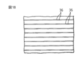
図18は従来の配向分割をした液晶表示装置の画面の一例を示す図である。図18では、図4を参照して説明した黒い線36が現れる。黒い線36は輝度の低下の原因となる。
図19は配向分割をし且つ第1及び第2の位相差板24,26を設けた液晶表示装置の画面の一例を示す図である。図18では、図4を参照して説明した黒い線36が現れる。図19においては、図18の黒い線36が解消されている。
【0038】
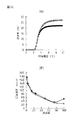
図20(A)は従来及び本発明の配向分割をした液晶表示装置の印加電圧と透過率との関係を示す図である。黒い点をプロットした曲線は従来の液晶表示装置に関し、白い点をプロットした曲線は本発明の液晶表示装置に関する。配向分割はともに線状構造物30とスリット38との組み合わせからなる(図5及び図6)ものであった。電圧が5.4Vのときには、透過率は1.19倍になった。図20(B)は応答性が改善されることを示している。
【0039】
図5から図14は図2から図4の配向分割をした液晶セルの変形例を示す図である。図5から図14に示した液晶セルは、図1の液晶セル12として採用可能であり、図15から図20を参照して説明した作用を含むものである。
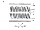
図5及び図6においては、第1の基板14は電極28及び電極28上に誘電体によって形成された線状構造物(リブ)30を有する。第2の基板16は電極32及び電極32に形成されたスリット38を有する。スリット38は、図2及び図3の線状構造物34と同様に延びるスリットベース部38aと、スリットベース部38aの延びる方向とは直交方向に延びる微細スリット部38bとを有する。スリットベース部38aは図3の線状構造物34と同様の作用をもつが、微細スリット部38bが表示ドメインを形成する部分にあることにより、電界歪みの影響が、特に表示ドメインを構成する液晶分子に高速に伝わるので、中間調の応答の性能を改善することができる。特に、微細スリット部38bの形状が、図6に示す三角形の集合のように基板面に平行方向性をもつ場合、応答速度の改善効果が高い。
【0040】
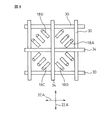
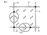
図7から図9においては、第1の基板14は電極28及び電極28上に誘電体によって形成された線状構造物(リブ)30を有し、第2の基板16は電極32及び電極32に形成された線状構造物(リブ)34を有する。この例では、第1の基板14の線状構造物30は格子状に配置され、第2の基板16の線状構造物34は第1の基板14の線状構造物30とはずらされて格子状に配置されている。このようにして、線状構造物30,34のクロス部分において液晶分子18A,18B,18C,18Dを含む4つの液晶配向領域が形成される。この場合、4つの液晶配向領域において液晶分子18A,18B,18C,18Dの配向方向が異なるので、配向分割の効果はさらに高くなる。ただし、第1及び第2の偏光板20,22の偏光軸20A,22Aは線状構造物30,34と平行に配置されるが、線状構造物30,34上には線状構造物30,34と平行に延び、且つ互いに逆方向に向いた液晶分子18P,18Qが存在する。液晶分子18P,18Qは、黒い線36の原因となり、且つ応答性を遅くする原因になるが、第1及び第2の位相差板24,26を設けることにより、上記したのと同様に輝度及び応答性を改善することができる。
【0041】
図10及び図11においては、第1の基板14は電極28を有し、線状構造物又はスリットはない。第2の基板16は電極32及び電極32に形成された魚の骨状のパターンのスリット38を有する。スリット38はスリットベース部38aと微細スリット部38bとからなる。液晶分子18A,18Bは互いに異なる方向に配向する。液晶分子18Rはスリットベース部38a上に位置する。
【0042】
図12から図14においては、第1の基板14は電極28を有し、線状構造物又はスリットはない。第2の基板16は電極32及び電極32に形成された魚の骨状のパターンのスリット38を有する。スリット38はスリットベース部38aと微細スリット部38bとからなる。微細スリット部38bは先端が細くなっている。液晶分子18A,18Bは互いに異なる方向に配向する。液晶分子18Rはスリットベース部38a上に位置する。
【0043】
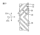
図21は配向分割した液晶セルの他の例を示す図である。液晶セル12は第1の基板14と第2の基板16との間に液晶層18を挟持してなり、第1及び第2の位相差板(24,26並びに第1及び第2の偏光板20,22が液晶セル12の両側に配置される(図1参照)。第1の基板14はカラーフィルタ基板であり、第2の基板16はTFT基板である。液晶セル12は15インチXGAの液晶パネルを構成し、画素ピッチは297μmである。
【0044】
1画素電極19(電極32)に対して、第1の基板14の線状構造物30は屈曲して形成され、第2の基板16のスリット38も屈曲して形成されている。この場合には、4つの分割された配向分割が実現される。線状構造物30はアクリル系感光性材料(例えばJSR製、PC−335)で作られ、線状構造物30の幅は10μm、高さは1.2μmである。スリット38の幅は10μmである。スリット38は画素電極19に形成されており、画素電極19を通って電流が流れるように、スリット38は断続的に形成されている。
【0045】
線状構造物30とスリット38との間の距離は25μmである。液晶セル12の厚さは4.64μmである。第1及び第2の位相差板(λ/4板)24,26はPC(ポリカーボネイト、例えば日東電工製のNRF−RF01A)を使用した。位相差は140nmである。ただし、その他の材料からなる位相差板(例えばアートンフィルム)を使用することもできる。また、第1及び第2の偏光板20,22は日東電工製のG1220DUを使用した。
【0046】
偏光板20,22を十字配置(図21の紙面において偏光軸20A,22Aが垂直及び水平に配置、この例では偏光軸20A,22Aが主たる液晶ダイレクタに対して45°になる)した場合には、白透過率が6.43パーセントであった。同様の構成において、偏光板20,22を45°の配置(例えば図21において偏光軸20A,22Aが垂直及び水平に対して45°に配置)した場合には、白透過率が6.58パーセントであった。なお、偏光板20,22の配置は十字配置及び45°の配置に限定されるものではなく、任意に設定することができる。一方、位相差板24,26のない従来の液晶表示装置では、十字配置の場合に白透過率が5.05パーセントであった。
【0047】
実施例においては線状構造物30とスリット38との間の間隙距離は25μmであるが、この間隙距離は変えることができる。第1及び第2の位相差板(λ/4板)24,26のない従来の配向分割した液晶表示装置では、この間隙距離が狭くなると、応答速度が上がるが、透過率が低下し、この間隙距離が広くなると、透過率が上がるが、応答速度が低下するという問題があった。これらはいずれも液晶分子の配向方位または配向方位の変化による透過率の低下又は変化に起因するものである。本発明においては、透過率が液晶分子の配向方位に依存しないため、間隙距離の変化に対する透過率の低下や応答速度の低下の影響は従来よりも小さい。そのため、動画対応用の液晶表示装置又は高輝度対応用の液晶表示装置などの用途に応じて、従来では適用できなかった狭い間隙又は広い間隙の液晶パネルを使用することができるようになる。
【0048】
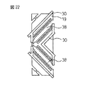
図22は配向分割した液晶セルの他の例を示す図である。1画素電極19に対して、第1の基板14の線状構造物30は屈曲して形成され、第2の基板16のスリット38も屈曲して形成されている。スリット38は図6に示したものと同様である。この場合には、4つに分割された配向分割が実現される。線状構造物30及びスリット38の幅は10μmである。微細スリット部のピッチは6μm、長さは15μmである。
【0049】
液晶セル12の厚さは4.26μmである点を除くと、液晶セル12は図21とほぼ同じ条件で製造される。偏光板20,22を十字配置した場合には、白透過率が5.74パーセントであった。同様の構成において、偏光板20,22を45°配置した場合には、白透過率が5.88パーセントであった。一方、位相差板24,26のない従来の液晶表示装置では、偏光板20,22を十字配置した場合に白透過率が4.47パーセントであった。この例では、セル厚が図21の例よりも薄いため、液晶層18のリターデーションが小さくなり、透過率の絶対値は若干低いが、位相差板を設けたことによる透過率の改善効果は図21の例と同様に高い。
【0050】
図23は配向分割した液晶セルの他の例を示す図である。第1の基板14は線状構造物30を有し、第2の基板16のスリット38を有する。線状構造物30及びスリット38は図7から図9に示す液晶セル12の線状構造物30,34と同様に格子状に配置される。線状構造物30の幅は8μm、高さは0.75μmである。スリット38の幅は8μmである。セル厚は4.02μmである。偏光板20,22を十字配置した場合には、白透過率が5.86パーセントであった。偏光板20,22を45°で配置した場合には、白透過率が5.78パーセントであった。一方、位相差板24,26のない従来の液晶表示装置では、十字配置した場合に白透過率が4.48パーセントであった。
【0051】
図24は配向分割した液晶セルの他の例を示す図である。この例は図11に示された魚の骨状のパターンのスリット38に類似した2つの魚の骨状のパターンのスリット38A,38Bを含む。セル厚は3.86μmである。その他の条件は図21の例と同様である。偏光板20,22を十字配置した場合には、白透過率が6.26パーセントであった。同様の構成において、偏光板20,22を45°で配置した場合には、白透過率が6.06パーセントであった。一方、位相差板24,26のない従来の液晶表示装置では、十字配置した場合に白透過率が5.12パーセントであった。
【0052】
図25は図24の構造の配向分割で到達透過率と立ち上がり時間との関係を示す図である。黒三角をプロットした曲線は図24の構造の配向分割で位相差板のないものを示し、白三角をプロットした曲線は図24の構造の配向分割で位相差板のあるものを示す。従来、この方式では中間調を含めた全階調での応答が数100msあり、液晶モニターなどの液晶応用装置には適していなかった。本発明を適用することによって、黒から白への応答が20ms、黒から中間調(25%)であっても90msの応答速度が実現され、液晶モニターなどの液晶応用装置に適用することができるようになった。
【0053】
図26から図28はセル厚と透過率との関係を示す図である。図26は平行な線構造物の配向分割(例えば図21)についてセル厚と透過率との関係を示す図である。図27は格子状の配向分割(例えば図23)についてセル厚と透過率との関係を示す図である。図28は魚骨状の配向分割(例えば図24)についてセル厚と透過率との関係を示す図である。
【0054】
これらの図において、四角をプロットした曲線は位相差板(λ/4)がなく、偏光板が十字配置の場合を示し、三角をプロットした曲線は位相差板(λ/4)があり、偏光板が十字配置の場合を示し、黒丸プロットした曲線は位相差板(λ/4)があり、偏光板が45度で配置の場合を示す、
図26では、四角をプロットした曲線でセル厚4.2μmの場合は透過率が4.4%である。これは出願人が使用している液晶表示装置と同等である。三角をプロットした曲線及び黒丸をプロットした曲線でセル厚4.2μmの場合は透過率が5.8%である。さらに、図27では、黒丸をプロットした曲線でセル厚4.2μmの場合は透過率が6.2%である。図28では、黒丸をプロットした曲線でセル厚4.2μmの場合は透過率が6.9%である。このような、本発明によれば、透過率を向上させることができる。
【0055】
図29は配向分割した液晶セルの他の例を示す断面図、図30は図29の液晶セルを示す平面図である。液晶セル12は、電極を有する一対の基板14,16と、一対の基板に挟持された液晶層18とからなる。この液晶セル12は図1に示したように第1及び第2の偏光板20,22と、第1及び第2の位相差板24,26とともに使用される。この例では、液晶層18は垂直配向型の液晶からなるものではなく、水平配向型の液晶からなるものでもよい。ただし、液晶層18は、電圧印加時に液晶分子18Hの配向状態が極角変化及び方位角変化を伴って変化するように構成されている。基板14,16は配向制御のための線状構造物(リブ)30,34並びにスリット38を備えている必要はない。
【0056】
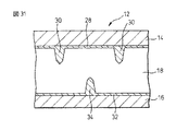
図31は本発明の第2実施例の液晶表示装置の導電性の線状構造物を有する液晶セルを示す図である。液晶表示装置10は、第1の基板14と第2の基板16との間に液晶層18を挟持してなる液晶セル12と、第1及び第2の偏光板20,22と、第1及び第2の位相差板24,26とからなる(図1参照)。
第1の基板14は線状構造物30を有し、第2の基板16は線状構造物34を有する。線状構造物30,34はこれまで説明したように互いに平行に交互に配置される(例えば図3参照)。線状構造物30,34は格子状に、あるいは魚骨状に配置されることもできる。
【0057】
線状構造物30,34は導電性の構造物であり、図31においては、線状構造物30は第1の基板14の電極28と同じ金属材料で形成され、線状構造物34は第2の基板16の電極32と同じ金属材料で形成される。例えば、電極28,32を形成する前に、基板上に予め線状の突起を形成しておき、その上にITOで電極28,32を形成する。あるいは、電極28,32の上に導電性の樹脂(カーボンなどの導電性粒子が混合されている樹脂)で線状構造物30,34を形成する。線状構造物30,34の高さは0.1μm〜セル厚の半分程度にする。一例においては、線状構造物30,34の高さは1.5μmである。電極28,32及び線状構造物30,34の上には垂直配向膜が塗布される。
【0058】
これまで説明した例では、線状構造物30,34は誘電体で作られている。線状構造物30,34が誘電体で作られていると、電極28,32間に印加される電圧の一部が誘電体で吸収され、その分だけ液晶に印加される電圧が低下する。そのため、電圧印加時の液晶分子の傾斜が不十分になり、透過率が低下する。この例においては、線状構造物30,34は導電性であるので、電極28,32間に印加される電圧の一部が吸収されることがなく、液晶に印加される電圧が低下することがなく、電圧印加時の液晶分子の傾斜が十分になり、透過率が低下することがない。
【0059】
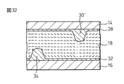
図32は図31の液晶セルを使用した場合の液晶の配向状態を示す図である。電圧を印加したときに、液晶分子が十分に傾斜しているのが分かる。
図33は導電性の線状構造物を有する液晶セルの他の例を示す図である。第1の基板14は線状構造物30及びスリット38を有し、第2の基板16は線状構造物又はスリットを有しない。ただし、第1の基板14は線状構造物30を有し、第2の基板16はスリット38を有する構成とすることもできる。
【0060】
図34は図33の液晶セルを使用した場合の液晶の配向状態を示す図である。電圧を印加したときに、スリット38の近傍においては、液晶分子が十分に傾斜しないが、線状構造物30の近傍の液晶分子は十分に傾斜しているのが分かる。図33の構成でも、良好な配向分割を達成することができ、且つ透過率を向上させることができる。
【0061】
図35は導電性の線状構造物を有する液晶セルの他の例を示す図である。第1の基板14は線状構造物30M及び線状構造物30Dを有し、第2の基板16は線状構造物又はスリットを有しない。線状構造物30Mは導電性であり、線状構造物30Dは誘電体である。線状構造物30Mが広い間隔で配置される場合に、線状構造物30Dは線状構造物30Mの間に配置される。
【0062】
図36は図35の液晶セルを使用した場合の液晶の配向状態を示す図である。電圧を印加したときに、線状構造物30Dの近傍においては、液晶分子が十分に傾斜しないが、線状構造物30Mの近傍の液晶分子は十分に傾斜しているのが分かる。図35の構成でも、良好な配向分割を達成することができ、且つ透過率を向上させることができる。
【0063】
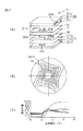
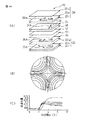
図37は本発明の第3実施例の液晶表示装置を示す図である。図37(A)は液晶表示装置の構成を示し、図37(B)は斜め方向から画面を見たときの表示のコントラストを示し、図37(C)は印加電圧と透過光量との関係を示す図である。図37(A)に示すように、液晶表示装置10は、液晶セル12と、第1及び第2の偏光板20,22と、第1及び第2の位相差板24,26とからなる。
【0064】
第1及び第2の位相差板24,26の各々は、基板面と平行な面内に光軸24A,26Aを有しかつ位相差がほぼλ/4である。第1の位相差板24の光軸24Aは第2の位相差板26の光軸26Aと直交している。第1及び第2の偏光板20,22の偏光軸20A,22Aは第1及び第2の位相差板24,26の光軸24A,26Aに対して45°で配置される。第1及び第2の位相差板24,26は面内の位相差が120nm以上、160nm以下である。好ましくは、第1及び第2の位相差板24,26は面内の位相差が130nm以上、145nm以下である。
【0065】
第1の偏光板20は偏光層(例えばPVA+ヨウ素)20pと、偏光層20pの両側を覆う保護層(例えばTAC、トリアセチルセルロース)20q,20rとからなる。同様に、第2の偏光板22は偏光層(例えばPVA+ヨウ素)22pと、偏光層22pの両側を覆う保護層(例えばTAC、トリアセチルセルロース)22q,22rとからなる。
【0066】
液晶セル12は図1に示したように第1の基板14と第2の基板16との間に液晶層18を挟持してなる。液晶層18は垂直配向型の液晶からなる。そして、液晶セルは少なくとも一方の基板の電極に設けられた構造物又はスリットを含み、この構造物又はスリットの一方側に位置する液晶分子の配向状態が該構造物又はスリットの他方側に位置する液晶分子の配向状態とは異なっている。構造物又はスリット及びスリットについてはすでに説明したあらゆるものを使用することができる。
【0067】
図38は図37で使用した配向分割の例を示し、配向分割は、第1の基板14の電極の上に設けられた屈曲した線状構造物30と、第1の基板14の電極の上に設けられた屈曲した線状スリット38とからなる。このような配向分割では、矢印18C,18D,18E,18Fで示されるように、液晶分子は4つの方向に配向する。すなわち、4分割の配向分割が達成される。図38においては、ゲートバスライン40、データバスライン42、TFT44、及び補助容量電極46が示されている。偏光板20,22は十字配置で配置されている。
【0068】
図37(A)及び図38に示される構成の場合に、コントラストは図37(B)に示されるようになり、このときには、コントラストが最も保たれる方位は上下左右から反時計回りに約30°回転した。その視角特性としては、コントラスト10以上の範囲として傾き角40°以上となった。
図39は図37の液晶表示装置の変形例を示す図である。図39の液晶表示装置10は図37の液晶表示装置とほぼ同様の構成を示すが、負の位相差を有する補償フィルム(例えばTACフィルム)48が第1の位相差板(λ/4)24と液晶セル12との間に積層され、負の位相差を有する補償フィルム(例えばTACフィルム)50が第2の位相差板(λ/4)と液晶セル12との間に積層されている。補償フィルム48,50が積層されることにより、液晶層18のもつ正の位相差が補償され、コントラスト5以上の範囲が広がっている(図39(B))。コントラストが10以上となる視角範囲を広げることができ、傾き角50°の程度までコントラストが10以上であった。ただし、図39(C)のT−V特性においては、電圧を高くすると、輝度が下がる傾向が強まっており、その結果階調反転が生じやすくなっている。
【0069】
図40は負の位相差を有する補償フィルム48,50の設置位置を液晶セル12の近傍ではなくて、液晶セル12から遠い側に設置した場合を示す。補償フィルム48,50を追加したにもかかわらず、その視角特性の改善度合は図39に比べると劣っていた。このことから、負の位相差をもつ補償フィルム48,50を液晶セル12に近傍して設定することが好ましいことが分かった。
【0070】
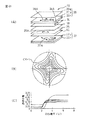
図41は図37の液晶表示装置の変形例を示す。偏光板20,22の設定角度を図37から変えた。偏光板20,22を45°,135°方位に設定し、λ/4板24,26を十字に配置した。この時の等コントラスト曲線を見ると、図37の実施例と比較してコントラスト5以上となる範囲が広がっていることが分かる(図41(B))。また、T−V特性を見ると、高電圧側での輝度の低下が少なく、階調特性に優れていることが分かる(図41(C))。
【0071】
図42は図37の液晶表示装置の変形例を示す。液晶セル12とλ/4板24,26との間に負の補償フィルム48,50としてTACフィルムを積層した。これにより、コントラストの得られる視角範囲を広げることが出来た。(図41(B)、図42(B)のデータを比較参照)。但し、T−V特性を見ると、高電圧側での輝度の低下が見られ、階調反転は生じやすくなっている。
【0072】
図43は図37の液晶表示装置の変形例を示す。偏光板20,22の角度を最適化して、コントラストが最大となる視角方位を上下左右方向とした。ここで、位相差板(λ/4)24,26は完全な一軸フィルムを想定して計算した。入射側の偏光板22の吸収軸22Aの方向を145度方位とし、クロスニコル配置とした。偏光板22と近接する位相差板26の遅相軸26Aの方向を10度方位、即ち入射側の偏光板22の吸収軸22Aと相対的に45度の角度に設定した。対となる位相差板24の遅相軸24Aは100度方位、即ち、一対の位相差板24,26の遅相軸24A,26Aが直交するように設定した。補償フィルム48,50はない。
【0073】
図44は図43の液晶表示装置の変形例を示す。図43に示した偏光板20,22と位相差板24,26との設定角度差は固定しておき、液晶セル12と位相差板24,26との間に負の補償層48,50としてTACフィルムを積層した。これにより、視角範囲を図43に比較して広げることが出来た。
以上の説明では4分割配向についての実施例を説明した。以下、2分割配向に適用した場合について説明する。2分割の配向としては、上下2分割であって、液晶分子は電圧の印加とともに画素の上半分は下方位、下半分は上方位に傾く。
【0074】
図45は図37の液晶表示装置の変形例を示す。偏光板20,22を十字に設定し、位相差板24,26を45,135度方位に設定した。
図46は図45の液晶表示装置の変形例を示す。図37は4分割配向であるのに対して、図46は2分割配向であり、偏光板やフィルムの配置は図37と同じである。液晶セル12と位相差板24,26との間に負の補償層48,50としてTACフィルムを積層した。
【0075】
図47は図37の液晶表示装置の変形例を示す。偏光板20,22及び位相差板24,26の設置角度を変えて、視角特性を上下対称、左右対称にした。入射側の偏光板22の吸収軸22Aを120度方位、近接する位相差板26の遅相軸26Aを75度方位、対となる位相差板24の遅相軸24Aを−15度方位、出射側の偏光板20の吸収軸20Aを30度方位に設定した。
【0076】
図48は図47の液晶表示装置の変形例を示す。液晶セル12と位相差板24,26との間に負の補償層48,50としてTACフィルムを積層した。入射側の偏光板22の吸収軸22Aを155度方位、近接する位相差板26の遅相軸26Aの方位を20度、対となる位相差板24の遅相軸24Aを110度方位、出射側の偏光板20の吸収軸20Aを65度方位に設定した。これにより対称性は崩れたものの、広いコントラスト範囲を実現することが出来た。
【0077】
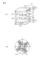
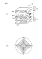
図49は図37の液晶表示装置の変形例を示す。液晶層18の位相差を完全に消し、偏光板20,22の視角範囲を最大にするとともに、位相差板24,26起因の光漏れを最低限に抑える構成を考案した。バックライト側の偏光板22から構成を述べる。偏光板22の吸収軸22Aの角度を135度方位に設定し、次にλ/4板26をその遅相軸26Aを0度方位として設定し、次に4分割配向の液晶セル12をその配向方向を45,135,225,315度方位に設定し、次に垂直配向している液晶層18の複屈折を完全に消すために屈折率の関係が座布団のようになっている光学層52を設定し(液晶層のΔndと同一のΔnd)、次にλ/4板24をその遅相軸24Aを90度方位にして設定し、次に遅相軸が基板に対して垂直な一軸光学層(図中ではラグビーボール型と表現している)54を設定し、次に一軸フィルムとして位相差が140nmのフィルム56をその遅相軸56Aを135度方位として設置し、偏光板20をその吸収軸20Aを45度方位にして設置した。この時、上下左右対称の特性となり、且つ、コントラスト10以上の範囲は斜め45度方位でも50度を実現することが出来た。ここで、座布団のようになっている光学層52の位相差は液晶層18の位相差と同一が望ましいが、望ましくは±10%以内の違いに設定されてなる時に特にコントラストの良好な範囲を広げることができた。
【0078】
図50は図49の液晶表示装置の変形例を示す。図49の実施例とは偏光板20,24の設置角度を変更している。バックライト側の偏光板22から構成を述べる。偏光板22の吸収軸22Aの角度を0度方位に設定し、次にλ/4板26をその遅相軸を45度方位として設定し、次に4分割配向の液晶セル12をその配向方向を45,135,225,315度方位に設定し、次に垂直配向して液晶層の複屈折を完全に消すために屈折率の関係が座布団のようになっている光学層52を設定し(液晶層のΔndと同一のΔnd)、次にλ/4板24をその遅相軸24Aを135度方位にして設定し、次に遅相軸が基板に対して垂直な一軸光学層(図中ではラグビーボール型と表現している)54を設定し、次に一軸フィルムとして位相差が140nmのフィルム56をその遅相軸56Aを0度方位として設定し、板20をその吸収軸20Aを90度方位にして設置した。この時、コントラストが最も保たれる方位は上下左右方向からずれて斜め45度方位などとなったが、コントラストが5となってしまう傾き角は最悪の場合でも75度と広い角度を実現することが出来た。
【0079】
図51は図37の液晶表示装置の変形例を示す。図49の実施例では配向は4分割されていたが、本実施例においては、2分割されている。基本的には図49の実施例に対して、配向方向が90度、270度の二方向の配向分割になっており、偏光板20,22、視角改善用フィルム52,54,56、λ/4板などの配置は図49の実施例と同一である。その視角特性を見ると、コントラスト比の視角特性について見れば、4分割された図49の実施例を上回る特性が得られている。一方、T−V特性を見ると、電圧の印加に伴うT−V特性のうねりは、図49に比べて大きいものとなっており、中間調を表示した時の視角特性は劣ることが分かる。しかしながら、2分割は4分割に比べて作りやすい構成も考えられる。
【0080】
図52は図37の液晶表示装置の変形例を示す。図50の実施例に対して、偏光板20,22、補償フィルム52,54,56等の設定角度を変えず、液晶セル12の配向方位を2分割とし、その方位としては、90度、270度方位に設定した。
図53は図37の液晶表示装置の変形例を示す。これまでの実施例においては、λ/4板24,26として、一軸延伸フィルム、特に、光学的に一軸のフィルムを用いている。これに対して、この実施例においては、λ/4板24,26として負の位相差(=(nx+ny)/2−nz)がゼロのフィルムを用いた。この時のコントラスト比の視角特性(図53(B))を見るとコントラスト10の線が全く見られず、全方位傾き角80度以内において、良好な視角特性の実現されていることが分かる。この負の位相差が0となるフィルムとしては、日東電工からNZフィルム、住友化学よりSZフィルムという名称にて市販されているものを用いることが出来た。ここで、この負の位相差(=(nx+ny)/2−nz)であるが、0±20nmに設定したときに特に広い視野角を実現することが出来た。また、更に、片側の偏光板の吸収軸とその遅相軸を直交させて位相差フィルム56を偏光板20に近接させて設定した。その位相差フィルム56の面内位相差の値としては、一対の偏光板の双方に近接して設ける場合には、25nm以上70nm以下、片側の偏光板にのみ近接して設ける場合には60nm以上160nm以下に設定した(例では140nm)。また、更に、基板に対して垂直な方向に正の光学的異方性を有するフィルム52を重ねた、その位置としては、λ/4板26と偏光板22との間に設定した。そして、その位相差の値としては、80nm以上、300nm以下とした。望ましくは90nm±10nmに設定した。このとき、図53(B)に示すような特に広い視野角を実現することが出来た。
【0081】
図54に4分割配向を実現するにあたっての配向規制方向と、その時に実現される液晶分子の配向方向との関係を示す。実線の矢印18I,18JはTFT基板側の液晶分子を倒させる方位を示しており、点線の矢印18K,18LはCF基板側の液晶分子を倒させる方位を示している。これらの配向規制手段によって、液晶分子を倒れさせる働きは太い矢印18C,18D,18E,18Fのようになる。このような配向規制方位によって、結果として得られる液晶の配向方位を太い矢印18Mで示す。ここで、特徴的なのは、太い矢印18C,18D,18E,18Fと、太い矢印18Mとの方向が一致しない点である。ここで、太い矢印18C,18D,18E,18Fで示される配向規制方位の丁度中間の領域においては、液晶分子の配向はその二等分される方位を向くこととなり、画素全体を見ると、丁度画素の中心に向かって全体的にチューリップの花弁のように倒れる(あるいは外に向かって咲く)ようになる。
【0082】
この時に、偏光板を十字に設定した時の正面での光透過量の分布を図55に示す。このように、画素の中央に十字に黒い領域が存在することなり、明るい表示が得られない。このような場合に対してλ/4板を液晶層の両側に設定した場合には、明るい表示が実現されることとなる。
図54に示される配向規制の方法としては、光配向、ラビングなどを用いた。以上説明したように、本発明を用いることにより、明るい表示を実現できるとともに、視野角の広い液晶ディスプレイを実現することが出来た。
【0083】
図56は本発明の第4実施例の液晶表示装置を示す図である。図57は図56の特定方向散乱フィルムの作用を説明する図である。図58は配向分割された液晶表示装置の液晶分子の配向及び透過率を示す図である。図56において、液晶表示装置10は、液晶セル12と、第1及び第2の偏光板20,22と、特定方向散乱フィルム60と、視角改善フィルム62とからなる。偏光板20,22は図39に示したように偏光層20p,22pと、保護層20q,20r,22q,22rとからなるものである。図56に示す保護層20rは偏光板20の一部を構成するものである。
【0084】
液晶セル12は図1に示したように第1の基板14と第2の基板16との間に液晶層18を挟持してなる。液晶層18は垂直配向型の液晶からなる。そして、液晶セル12は配向分割されている。すなわち、液晶セル12は、少なくとも一方の基板の電極に設けられた構造物又はスリットを含み、この構造物又はスリットの一方側に位置する液晶分子の配向状態が該構造物又はスリットの他方側に位置する液晶分子の配向状態とは異なっている。構造物又はスリット及びスリットについてはすでに説明したあらゆるものを使用することができる。
【0085】
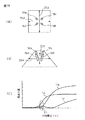
図58は4つの異なった配向状態の液晶分子18c,18d,18e,18f及び印加電圧と透過光量との関係を示す図である。図58(A)は例えば図58(C)の比較的に低い電圧V1を印加し且つ画面を法線方向から見た場合の液晶分子18c,18d,18e,18fの配向状態を示し、図58(B)は同じ電圧V1を印加し且つ画面を斜め方向から見た場合の液晶分子18c,18d,18e,18fの配向状態を示している。図58(C)において、曲線TAは図58(B)の液晶分子18cの配向についてのT−V曲線であり、曲線TFは図58(B)の液晶分子18fの配向についてのT−V曲線であり、曲線TNは図58(A)の全ての液晶分子の平均的な配向についてのT−V曲線である。図58(C)から分かるように、比較的に低い電圧V1を印加し且つ画面を斜め方向から見た場合には、画面を法線方向から見た場合と比べて輝度が高くなる。比較的に低い電圧V1を印加した場合には、階調的に比較的に暗い表示を実現しようとしているのであるが、それにもかかわらず、一部の視角において白っぽい表示となってしまう。この現象は視角改善フィルム62を含む場合に顕著になる場合がある。
【0086】
図56の液晶表示装置10は特定方向散乱フィルム60を備えることによってこのような問題点を解決するのに適したものである。特定方向散乱フィルム60は特定の方向の散乱性が大きく、その他の方向の散乱性は比較的に小さい性質をもつのである。特定方向散乱フィルム60は例えば住友化学製のニミスティー等を利用することができる。
【0087】
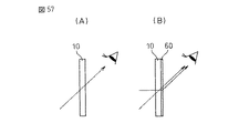
図57(A)は特定方向散乱フィルム60のない液晶表示装置10を斜め方向から見る場合を示し、図57(B)は特定方向散乱フィルム60のある液晶表示装置10を斜め方向から見る場合を示している。図57(A)においては、液晶セル12を斜めに透過した光が観視者の目に入り、観視者は上記したように白っぽい表示を見ることがある。図57(B)においては、特定方向散乱フィルム60はこの特定方向散乱フィルム60に法線方向に入射した光を斜め上方向に散乱させる性質を有し、液晶セル12を法線方向に透過した光及び液晶セル12を斜めに透過した光が観視者の目に入り、観視者は画面を法線方向から見るのに近い表示を見ることになる。液晶セル12を法線方向に透過した光及び液晶セル12を斜めに透過した光との間の視差を小さくするために、特定方向散乱フィルム60は光出射側の偏光板20に近く配置されるので好ましい。
【0088】
視角改善フィルム62は、例えば上記の実施例の位相差板(λ/4板)24,26であり、偏光板20,22と位相差板(λ/4板)24,26との組み合わせで円偏光を生成し、輝度の向上に寄与することは上記した通りである。なお、図56においては、視角改善フィルム62は一方の基板14側にのみ設けられているが、他方の基板16側にも設けられることができることは言うまでもない。さらに、視角改善フィルム62は、図39から図53に示したフィルム48,50,52,54,56とすることもできる。すなわち、視角改善フィルム62は、一軸延伸フィルム、二軸延伸フィルム、及び負の位相差を有するフィルム等で形成される。
【0089】
図59は図56の液晶表示装置の変形例を示す図である。図56においては、特定方向散乱フィルム60が光出射側の偏光板20に近く、視角改善フィルム62が基板14に近い配置となっていたのに対して、図59においては、特定方向散乱フィルム60が基板14に近く、視角改善フィルム62が光出射側の偏光板20に近い配置となっている。この例の作用は図59の例の作用と同様である。
【0090】
特定方向に光を散乱するフィルムの設置位置としては、液晶層に近接して視角改善フィルムを設置し、この視角改善フィルムと偏光層との間に光散乱フィルムを設置したときに特に良い視角特性が得られた。本来視角改善フィルムは液晶層に斜めに入射した光への液晶の光学的効果を消すためのものである。ところが、液晶層に近接して光散乱フィルムを設置してしまうと、液晶層に垂直に入射した光が散乱されて斜めに視角改善フィルムを通過することになる。この場合、液晶層に垂直に入射した光は何ら光学的作用を液晶層で受けていないにもかかわらず、視角改善フィルムは光学的効果を発揮する。すなわち、逆に光洩れを起こさせるように働いてしまう。
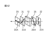
【0091】
図61は本発明の第5実施例の液晶表示装置を示す図である。図62は図61の液晶表示装置の偏光板の偏光軸及び位相差板の光学軸を説明する図である。液晶表示装置10は、液晶セル12と、第1及び第2の偏光板20,22と、第1及び第2の位相差板24,26とからなる。第1及び第2の位相差板24,26の各々は、基板面と平行な面内に光軸24A,26Aを有しかつ位相差がほぼλ/4である。第1の位相差板24の光軸24Aは第2の位相差板26の光軸26Aと直交している。第1及び第2の偏光板20,22の偏光軸20A,22Aは第1及び第2の位相差板24,26の光軸24A,26Aに対して45°で配置される。電極28と電極32との間に電圧を印加するようになっている。
【0092】
液晶セル12は第1の基板14と第2の基板16との間に挟持された液晶層18を有する。液晶層18は液晶ドロップレット70が樹脂72の中に分散している。液晶ドロップレット70と樹脂72とからなる液晶層18を有する液晶表示装置はポリマー分散型液晶表示装置と呼ばれる。ただし、本発明はポリマー分散型液晶表示装置に限定されるものではなく、液晶層18が液晶ドロップレット70が樹脂72の中に共存しているその他のタイプの液晶表示装置にも適用可能である。
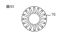
【0093】
図63は電圧不印加時の液晶ドロップレット70中の液晶分子の配向状態を示す図である。液晶分子はあらゆる配向方向に向いて配向している。この状態から電位を印加すると、液晶分子は液晶ドロップレット70中で基板面に対して垂直に配向するようになる。
図64は図63の液晶分子の電圧無印加時の配向状態のときの表示を示す図である。液晶分子は基板面に対してほぼランダムに配向しているので、偏光板20,22がクロスニコルで配置されていて、λ/4板が設置されている場合には、白表示を生成する。
【0094】
図65は偏光板20,22があり且つ位相差板24,26がない従来の液晶表示装置の表示を示す図である。図63に示されるように、液晶ドロップレット70a中で液晶分子はあらゆる配向方向に向いて配向しており、偏光板20,22の吸収軸20A,22Aは直交して配置されているので、液晶分子が吸収軸20A,22Aと同じ方向に配向しているところでは、表示は黒くなる。このことは、図4及び図9の黒い線36と同様である。
【0095】
本願の発明では、位相差板24,26を設けることにより、図65の黒い表示の部分を解消することができ、図64のように明るい表示を実現することができる。
ポリマー分散型液晶パネルを実現するために、フッ素樹脂と紫外線硬化型の樹脂とを混合し(混合比8:2程度)、極力液晶ドロップレット70の大きさを大きくとれるように工夫した。液晶は、正の誘電率異方性をもつもの、又は負の誘電率異方性をもつものを使用することができる。正の誘電率異方性をもつ液晶を用いた場合には、電圧不印加時に液晶分子は寝ていることが望まれるので、配向膜を塗布する必要はなく、洗浄した基板の間に液晶と樹脂との混合物を注入する。負の誘電率異方性をもつ液晶を用いた場合には、電圧印加時に液晶分子は寝るので、電圧不印加時に垂直に配向していることが必要である。このことから、基板上に垂直配向性を有するポリイミド膜を塗布する。
【0096】
液晶と樹脂との混合物を注入した後、紫外線を照射し、樹脂を硬化させた。この間に、液晶と樹脂とが分離し、液晶のドロップレット70が形成された。
図66は本発明の第6実施例の液晶表示装置を示す図である。図67は図66の液晶表示装置の偏光板の偏光軸及び位相差板の光学軸を説明する図である。液晶表示装置10は、液晶セル12と、第1及び第2の偏光板20,22と、第1及び第2の位相差板24,26とからなる。第1及び第2の位相差板24,26の各々は、基板面と平行な面内に光軸24A,26Aを有しかつ位相差がほぼλ/4である。第1の位相差板24の光軸24Aは第2の位相差板26の光軸26Aと直交している。第1及び第2の偏光板20,22の偏光軸20A,22Aは第1及び第2の位相差板24,26の光軸24A,26Aに対して45°で配置される。電極28と電極32との間に電圧を印加するようになっている。
【0097】
液晶セル12は第1の基板14と第2の基板16との間に挟持された液晶層18を有する。液晶層18は液晶74がポリマーネットワーク76の中に分散している。液晶74とポリマーネットワーク76とからなる液晶層18を有する液晶表示装置はポリマーネットワーク型液晶表示装置と呼ばれる。液晶は負の誘電率異方性を有する垂直配向型の液晶である。第1の基板14はカラーフィルタ基板であり、第2の基板16はTFT基板である。
【0098】
上記したように、垂直配向型の液晶を用い、線状構造物30,34や、スリット38を用いた配向分割では、電圧印加時に一部の液晶分子と偏光板の偏光軸とが一致すると、輝度が低下するという問題があり、位相差板(λ/4板)を設けることによって輝度を向上させることができる。しかし、より明るい画面が必要なノート型パソコン等の画面にこの技術を用いる場合、表示領域内に線状構造物30,34やスリット38があると、表示領域の開口率が減少し、十分な輝度を提供できない。そこで、バスラインや補助容量ライン上にのみ線状構造物30,34やスリット38を設けると、表示領域の開口率が増大し、十分な輝度を提供することができる。しかし、この場合には、線状構造物30,34同志の間隔又は線状構造物30とスリット38との間隔が広くなり過ぎ、液晶の傾斜の伝播に多大の時間がかかり、応答速度が低下する。この実施例の液晶表示装置はこの問題点を解決しようとするものである。
【0099】
ポリマーネットワーク76は液晶74の液晶分子のプレチルト及び電圧印加時の液晶分子の傾斜方向を規定するように形成されている(ポリマースタビライズと言う)。ポリマーネットワーク76は液晶性又は非液晶性モノマーが紫外線又は熱により重合してポリマー化したものであり、重合時に特定の方向性をもった構造として固化される。従って、ポリマーネットワーク76は液晶ドロップレット74の液晶分子をプレチルトを伴ってほぼ垂直方向に配向させ、そして、電圧を印加すると液晶分子はポリマーネットワーク76に規制された方向(プレチルトに従った方向)に応答性よく傾斜する。
【0100】
ポリマーネットワーク76を形成するモノマーは紫外線硬化型又は熱硬化型モノマーからなる。好ましくはポリマーネットワーク76を形成するモノマーは2官能アクリレート、又は2官能アクリレートと単官能アクリレートとの混合物である。好ましくは、ポリマーネットワーク76によって規制される液晶分子のプレチルト角は80°以上である。
【0101】
ポリマーネットワーク76の安定化処理は図68に示される方法により行われる。液晶性モノマーを一対の基板14,16の間に挿入してなる液晶セル12の電極28,32に電圧を印加しながら、液晶セル12に紫外線(UV)を照射し、液晶性モノマーを光重合させ、ポリマー化する。電圧を印加しながら重合させるので、通常の配向分割の液晶表示装置の使用状態と同様に、液晶分子は線状構造物30,34やスリット38に向かって配向する。
【0102】
安定化処理のための電圧印加を止めたときに、液晶分子は固化されたポリマーに規制されて所定の方向に配向した状態を維持し、こうして液晶はプレチルトする。このときに、線状構造物30,34やスリット38がなくても、バスラインや補助容量電極等の突起構造物が線状構造物30,34やスリット38と同等の作用をし、液晶はプレチルトする。このときの液晶分子の挙動には応答速度は問題ではなく、液晶分子は比較的に長い時間をかけてプレチルトすればよい。
【0103】
なお、ポリマーネットワーク76は固化した状態になると言っても、それは完全な固体とはなっていず、その後の液晶表示装置の使用において電圧を印加すると、液晶分子は基板面に対してプレチルトに従って傾斜する。このときにはすでに液晶分子は全体的にプレチルトしているので、応答速度は早い。
プレチルト角は、添加するモノマーの量及び光重合開始剤、UV照射量、及び印加電圧に依存する。垂直配向型液晶の特徴を維持するためには、プレチルト角は80°以上が望ましい。
【0104】
図69は液晶表示装置の使用時の階調と応答速度との関係を示す図である。曲線Xは本発明による応答速度を示し、曲線Yはポリマーネットワーク76を安定化処理しなかった場合の応答速度を示す。液晶性モノマーは1.8重量%のものであり、安定化のときの印加電圧は5.4ボルトであった。本発明によれば、液晶表示装置の表示の応答性がかなり向上することが分かる。
【0105】
図70は図66の液晶表示装置の配向分割のための構造を示す図である。カラーフィルタ基板14及びTFT基板16は電極28,32及び垂直配向膜29,33を有する。上記した実施例には配向膜は示されていないが、そのような実施例においても図70に示される垂直配向膜29,33と同様の配向膜が設けられる。さらに、図70においては、ゲートバスライン40及び補助容量電極46が示されている。
【0106】
図70(A)においては、線状構造物30,34及びスリット38は設けられていない。この場合には、上記安定化処理において、ゲートバスライン40及び補助容量電極46が突起状構造物として作用する。図70(B)においては、カラーフィルタ基板14にのみ線状構造物30が設けられている。線状構造物30は補助容量電極46に対応する位置に設けられており、表示領域の開口率に影響しない。
【0107】
図70(C)においては、カラーフィルタ基板14に線状構造物30が設けられ、TFT基板16に線状構造物34が設けられている。線状構造物30は補助容量電極46に対応する位置に設けられており、線状構造物34ゲートバスライン40に対応する位置に設けられており、表示領域の開口率に影響しない。
図70(D)においては、カラーフィルタ基板14に線状構造物30が設けられ、TFT基板16にスリット38が設けられている。線状構造物30及びスリット38は図70(C)の例よりも小さな間隔で設けられている。例えば、線状構造物30及びスリット38は図38に示すパターン又はその他のパターンで設けられることができる。
【0108】
【発明の効果】
以上説明したように、本発明によれば、広い視角の範囲にわたって良好な表示を見ることができ且つ輝度の高い液晶表示装置を得ることができる。
【図面の簡単な説明】
【図1】本発明の第1実施例の液晶表示装置を示す略図である。
【図2】図1の液晶セルを示す略断面図である。
【図3】図2の液晶セルの線状構造物及び液晶分子を示す略平面図である。
【図4】図3のA部分を示す詳細図である。
【図5】図2の液晶セルの変形例を示す略断面図である。
【図6】図5の液晶セルを示す略平面図である。
【図7】液晶セルの変形例を示す略断面図である。
【図8】図7の液晶セルを示す略平面図である。
【図9】図8の一部分を示す詳細図である。
【図10】液晶セルの変形例を示す略断面図である。
【図11】図9の液晶セルを示す略平面図である。
【図12】液晶セルの変形例を示す略断面図である。
【図13】図11の液晶セルを示す略平面図である。
【図14】図13のA部分を示す詳細図である。
【図15】位相差板(λ/4)の作用を説明する図であり、(A)は第1及び第2の偏光板の偏光軸、第1及び第2の位相差板の光軸、及び液晶層のダイレクタの関係を示し、(B)は第1の偏光板、第1の位相差板、液晶層、第2の位相差板、及び第2の偏光板を通る光の状態を示す図である。
【図16】液晶層のリターデーションがλ/2である場合の液晶層を通る偏光を示す図である。
【図17】液晶層のリターデーションがλ/4である場合の液晶層及び位相差板(λ/4)を通る偏光を示す図である。
【図18】従来の配向分割をした液晶表示装置の画面の一例を示す図である。
【図19】配向分割をし且つ第1及び第2の位相差板を設けた液晶表示装置の画面の一例を示す図である。
【図20】従来及び本発明の配向分割をした液晶表示装置の印加電圧と透過率との関係及び透過率と応答速度との関係を示す図である。
【図21】配向分割の他の例を示す図である。
【図22】配向分割の他の例を示す図である。
【図23】配向分割の他の例を示す図である。
【図24】配向分割の他の例を示す図である。
【図25】図24の構造の配向分割における到達透過率と立ち上がり時間との関係を示す図である。
【図26】平行な線状構造物の配向分割についてセル厚と透過率との関係を示す図である。
【図27】格子状の配向分割についてセル厚と透過率との関係を示す図である。
【図28】魚骨状の配向分割についてセル厚と透過率との関係を示す図である。
【図29】液晶セルの他の例を示す断面図である。
【図30】図29の液晶セルを示す平面図である。
【図31】本発明の第2実施例の液晶表示装置の導電性の線状構造物を有する液晶セルを示す断面図である。
【図32】図31の液晶セルを使用した場合の液晶の配向状態を示す図である。
【図33】導電性の線状構造物を有する液晶セルの他の例を示す断面図である。
【図34】図33の液晶セルを使用した場合の液晶の配向状態を示す図である。
【図35】導電性の線状構造物を有する液晶セルの他の例を示す断面図である。
【図36】 図35の液晶セルを使用した場合の液晶の配向状態を示す図である。
【図37】本発明の第3実施例の液晶表示装置を示す図である。
【図38】図37の配向分割の例を示す図である。
【図39】図37の液晶表示装置の変形例を示す図である。
【図40】図37の液晶表示装置の変形例を示す図である。
【図41】図37の液晶表示装置の変形例を示す図である。
【図42】図37の液晶表示装置の変形例を示す図である。
【図43】図37の液晶表示装置の変形例を示す図である。
【図44】図37の液晶表示装置の変形例を示す図である。
【図45】図37の液晶表示装置の変形例を示す図である。
【図46】図37の液晶表示装置の変形例を示す図である。
【図47】図37の液晶表示装置の変形例を示す図である。
【図48】図37の液晶表示装置の変形例を示す図である。
【図49】図37の液晶表示装置の変形例を示す図である。
【図50】図37の液晶表示装置の変形例を示す図である。
【図51】図37の液晶表示装置の変形例を示す図である。
【図52】図37の液晶表示装置の変形例を示す図である。
【図53】図37の液晶表示装置の変形例を示す図である。
【図54】図37の液晶表示装置の変形例を示す図である。
【図55】図54の液晶表示装置において偏光板を十字に設定したときの正面での光透過量の分布を示す図である。
【図56】本発明の第4実施例の液晶表示装置を示す図である。
【図57】図56の特定方向散乱フィルムの作用を説明する図である。
【図58】配向分割された液晶表示装置の液晶分子の配向及び透過率を示す図である。
【図59】図56の液晶表示装置の変形例を示す図である。
【図60】図56の液晶表示装置の変形例を示す図である。
【図61】本発明の第5実施例の液晶表示装置を示す図である。
【図62】図61の液晶表示装置の偏光板の偏光軸及び位相差板の光学軸を説明する図である。
【図63】図63の液晶ドロップレット中の液晶分子の配向状態を示す図である。
【図64】図63の液晶分子の配向状態のときの表示を示す図である。
【図65】従来の液晶表示装置の表示を示す図である。
【図66】本発明の第6実施例の液晶表示装置を示す図である。
【図67】図66の液晶表示装置の偏光板の偏光軸及び位相差板の光学軸を説明する図である。
【図68】図66の液晶セルの安定化処理を示す図である。
【図69】液晶表示装置の使用時の階調と応答速度との関係を示す図である。
【図70】図66の液晶表示装置の配向分割のための構造を示す図である。
【符号の説明】
10…液晶表示装置
12…液晶セル
14,16…基板
18…液晶層
20,22…偏光板
24,26…位相差板
30,34…線状構造物
38…スリット
48,50…補償フィルム
52,54,56…光学層
60…特定方向散乱フィルム
62…視角改善フィルム
70…液晶ドロップレット
72…樹脂
74…液晶
76…ポリマーネットワーク[0001]
BACKGROUND OF THE INVENTION
The present invention relates to a liquid crystal display device having improved viewing angle characteristics.
[0002]
[Prior art]
In a liquid crystal display device, it is known that the display contrast when viewing the screen from an oblique direction is different from the display contrast when viewing the screen from the front direction (viewing angle characteristics), and a liquid crystal having improved viewing angle characteristics. There is a need for a display device.
Japanese Patent Application Laid-Open Nos. 1-2270024 and 2000-29010 disclose a vertical alignment type liquid crystal cell, first and second polarizing plates disposed on both sides of the liquid crystal cell, a liquid crystal cell and a first polarizing plate. Disclosed is a liquid crystal display device including a first λ / 4 plate disposed between and a second first λ / 4 plate disposed between a liquid crystal cell and a second polarizing plate. ing. By providing the polarizing plate and the λ / 4 plate, it is possible to improve viewing angle characteristics when the screen is viewed from an oblique direction.
[0003]
However, a liquid crystal display device provided with a polarizing plate and a λ / 4 plate has a problem that the viewing angle range in which a display with good contrast can be seen is relatively narrow, although the viewing angle characteristics are improved.
Furthermore, there is alignment division as a technique for improving the viewing angle characteristics of a liquid crystal display device. In the alignment division, one pixel is divided into a plurality of regions having different alignment states of liquid crystal molecules so that a high-contrast display can be seen even when the screen is viewed from an oblique direction as when the screen is viewed from the front. It is a thing. In particular, the applicant of the present application has proposed a vertical alignment type liquid crystal display device provided with a structure or slit extending linearly on electrodes of a substrate sandwiching a liquid crystal layer.
[0004]
In this liquid crystal display device, many liquid crystal molecules are aligned substantially perpendicular to the substrate surface when no voltage is applied, but the liquid crystal molecules near the structure or slit are perpendicular to the wall surface of the structure or slit. There is a tendency to orient and pretilt the substrate surface. Therefore, when a voltage is applied, the liquid crystal molecules near the structure or the slit are tilted in a predetermined direction according to the pretilt, and many liquid crystal molecules are tilted according to the liquid crystal molecules near the structure or the slit.
[0005]
The alignment direction of the liquid crystal molecules located on one side of the structure or slit is opposite to the alignment direction of the liquid crystal molecules located on the other side of the structure or slit, and the two alignment states are different on both sides of the structure or slit. Areas are formed. Therefore, in this liquid crystal display device, it is possible to realize alignment division similar to that in which a pretilt is provided by rubbing without performing rubbing. By the orientation division, it is possible to obtain excellent viewing angle characteristics with high contrast in a wide viewing angle range. An alignment-divided liquid crystal display device is disclosed in, for example, Japanese Patent Application Laid-Open No. 11-352489.
[0006]
Japanese Patent No. 2945143 discloses a liquid crystal display device in which a polymer dispersion type liquid crystal panel is sandwiched between crossed Nicols polarizing plates. Japanese Patent Application Laid-Open No. 2000-347174 discloses a network-like polymer dispersion type liquid crystal display device.
[0007]
[Problems to be solved by the invention]
In such an alignment-divided liquid crystal display device, the alignment state of many liquid crystal molecules in one pixel at the time of voltage application is generally controlled according to a predetermined structure or slit, but some of the liquid crystal molecules in one pixel are controlled. The orientation state may not be controlled by a predetermined structure or slit. For example, liquid crystal molecules in the vicinity of a bus line in the periphery of a pixel tend to be aligned perpendicular to the wall surface of the bus line, and the alignment state of the liquid crystal molecules is controlled according to a predetermined structure or slit Unlike the molecular orientation, it may cause a decrease in luminance. Further, the liquid crystal molecules on the predetermined structure or slit are aligned in parallel with the predetermined structure or slit. The polarizing plate is arranged such that the polarization axis is 45 ° with respect to the director of the liquid crystal molecules when a voltage is applied, but some of the liquid crystal molecules are parallel to the polarization axis, causing a reduction in luminance.
[0008]
An object of the present invention is to provide a liquid crystal display device that can display a good display over a wide range of viewing angles and has high luminance.
[0009]
[Means for Solving the Problems]
A liquid crystal display device according to a first aspect of the present invention includes a liquid crystal cell comprising a pair of substrates having electrodes, a liquid crystal layer sandwiched between the pair of substrates, and first and first liquid crystals arranged on both sides of the liquid crystal cell. Two polarizing plates, a first retardation plate disposed between the liquid crystal cell and the first polarizing plate, and a second retardation plate disposed between the liquid crystal cell and the second polarizing plate, Each of the first and second retardation plates has an optical axis in a plane parallel to the substrate surface and has a retardation of approximately λ / 4, and the light of the first retardation plate The axis is orthogonal to the optical axis of the second retardation plate, and the polarization axes of the first and second polarizing plates are 45 ° with respect to the optical axes of the first and second retardation plates. The liquid crystal cell is characterized in that the orientation state of liquid crystal molecules changes with polar angle change and azimuth angle change when a voltage is applied.
[0010]
According to this configuration, it is possible to obtain a liquid crystal display device that can display a good display over a wide range of viewing angles and has high luminance.
In addition, when the liquid crystal molecules are arranged horizontally or inclined with respect to the substrate surface, the transmittance is improved if the orientation state of the liquid crystal molecules has an azimuth distribution.
A liquid crystal display device according to a second aspect of the present invention includes a liquid crystal cell comprising a pair of substrates having electrodes, a liquid crystal layer sandwiched between the pair of substrates, and first and first liquid crystals arranged on both sides of the liquid crystal cell. Two polarizing plates, a first retardation plate disposed between the liquid crystal cell and the first polarizing plate, and a second retardation plate disposed between the liquid crystal cell and the second polarizing plate, Each of the first and second retardation plates has an optical axis in a plane parallel to the substrate surface and has a retardation of approximately λ / 4, and the light of the first retardation plate The axis is orthogonal to the optical axis of the second retardation plate, and the polarization axes of the first and second polarizing plates are 45 ° with respect to the optical axes of the first and second retardation plates. And the liquid crystal of the liquid crystal cell is a vertical alignment type liquid crystal, and the liquid crystal cell includes a structure or a slit provided on an electrode of at least one substrate, the structure or the slit The alignment state of the liquid crystal molecules located on one side of the substrate is different from the alignment state of the liquid crystal molecules located on the other side of the structure or slit, and at least one of the pair of substrates is a conductive linear structure It is characterized by having.
[0011]
According to this configuration, it is possible to obtain a liquid crystal display device that can display a good display over a wide range of viewing angles and has high luminance.
According to a third aspect of the present invention, there is provided a liquid crystal display device comprising: a liquid crystal cell comprising a pair of substrates having electrodes; a liquid crystal layer sandwiched between the pair of substrates; and first and first liquid crystals disposed on both sides of the liquid crystal cell. Two polarizing plates, a first retardation plate disposed between the liquid crystal cell and the first polarizing plate, and a second retardation plate disposed between the liquid crystal cell and the second polarizing plate, Each of the first and second retardation plates has an optical axis in a plane parallel to the substrate surface and has a retardation of approximately λ / 4, and the light of the first retardation plate The axis is orthogonal to the optical axis of the second retardation plate, and the polarization axes of the first and second polarizing plates are 45 ° with respect to the optical axes of the first and second retardation plates. And the liquid crystal of the liquid crystal cell is a vertical alignment type liquid crystal, and the liquid crystal cell includes a structure or a slit provided on an electrode of at least one substrate, the structure or the slit The alignment state of the liquid crystal molecules located on one side of the liquid crystal is different from the alignment state of the liquid crystal molecules located on the other side of the structure or slit, and the in-plane retardation of the retardation plate is 120 nm or more and 160 nm or less. It is characterized by being.
[0012]
According to this configuration, it is possible to obtain a liquid crystal display device that can display a good display over a wide range of viewing angles and has high luminance.
A liquid crystal display device according to a fourth aspect of the present invention includes a liquid crystal cell including a pair of substrates having electrodes, a liquid crystal layer sandwiched between the pair of substrates, and a film that scatters light in a specific direction, The liquid crystal of the liquid crystal cell is a vertical alignment type liquid crystal, and the liquid crystal cell includes a structure or a slit provided on an electrode of at least one substrate, and an alignment state of liquid crystal molecules located on one side of the structure or the slit is It is different from the alignment state of the liquid crystal molecules located on the other side of the structure or the slit.
[0013]
According to this configuration, it is possible to obtain a liquid crystal display device that can display a good display over a wide range of viewing angles and has high luminance.
According to a fifth aspect of the present invention, there is provided a liquid crystal display device comprising: a liquid crystal cell comprising a pair of substrates having electrodes; a liquid crystal layer sandwiched between the pair of substrates; and first and first liquid crystals disposed on both sides of the liquid crystal cell. Two polarizing plates, a first retardation plate disposed between the liquid crystal cell and the first polarizing plate, and a second retardation plate disposed between the liquid crystal cell and the second polarizing plate, Each of the first and second retardation plates has an optical axis in a plane parallel to the substrate surface and has a retardation of approximately λ / 4, and the light of the first retardation plate The axis is orthogonal to the optical axis of the second retardation plate, and the polarization axes of the first and second polarizing plates are 45 ° with respect to the optical axes of the first and second retardation plates. And the liquid crystal layer of the liquid crystal cell includes liquid crystal and a resin coexisting with the liquid crystal.
[0014]
According to this configuration, it is possible to obtain a liquid crystal display device that can display a good display over a wide range of viewing angles and has high luminance.
A liquid crystal display device according to a sixth aspect of the present invention includes a liquid crystal cell including a pair of substrates having electrodes, a liquid crystal layer sandwiched between the pair of substrates, and first and first liquid crystals arranged on both sides of the liquid crystal cell. Two polarizing plates, a first retardation plate disposed between the liquid crystal cell and the first polarizing plate, and a second retardation plate disposed between the liquid crystal cell and the second polarizing plate, Each of the first and second retardation plates has an optical axis in a plane parallel to the substrate surface and has a retardation of approximately λ / 4, and the light of the first retardation plate The axis is orthogonal to the optical axis of the second retardation plate, and the polarization axes of the first and second polarizing plates are 45 ° with respect to the optical axes of the first and second retardation plates. The liquid crystal of the liquid crystal cell is a vertically aligned liquid crystal, a polymer network is formed in the liquid crystal layer of the liquid crystal cell, and the liquid crystal molecules are pre-tilted and the liquid crystal molecules are The inclination direction is defined by a polymer network.
[0015]
According to this configuration, it is possible to obtain a liquid crystal display device that can display a good display over a wide range of viewing angles and has high luminance.
[0016]
DETAILED DESCRIPTION OF THE INVENTION
Embodiments of the present invention will be described below with reference to the drawings.
FIG. 1 is a diagram showing a liquid crystal display device according to a first embodiment of the present invention. The liquid
[0017]
Each of the first and
[0018]
The
FIG. 2 is a schematic sectional view showing the
[0019]
Although only two
[0020]
In a vertical alignment type liquid crystal display device, generally, liquid crystal molecules are aligned substantially perpendicular to the substrate surface when no voltage is applied, and the liquid crystal molecules are inclined with respect to the substrate surface when a voltage is applied. With the
[0021]
The alignment direction of the
[0022]
In other words, in a general liquid crystal display device, when the screen is viewed from the major axis direction of tilted liquid crystal molecules, the display appears whitish, and when the screen is viewed from the axial direction with respect to the major axis direction of tilted liquid crystal molecules, the display is displayed. Looks dark. In the alignment division, the
[0023]
FIG. 4 is a detailed view showing part A of FIG. In such an alignment-divided liquid crystal display device, the alignment state of many liquid crystal molecules in one pixel when a voltage is applied is generally controlled according to
[0024]
However, the alignment state of some liquid crystal molecules in one pixel when a voltage is applied may not be controlled by the
[0025]
The
[0026]
Furthermore, since the tilt direction of the
[0027]
Although the liquid crystal display device having the
[0028]
The inventor of the present application, as shown in FIG. 1, reduces the luminance and the response of the alignment-divided liquid crystal display device as shown in FIG. 1 by the first retardation plate (λ / 4) 24 and the second retardation plate. It has been found that it is eliminated by providing the retardation plate (λ / 4) 26.
FIG. 15 is a view for explaining the operation of the phase difference plate (λ / 4) 24. In FIG. 15A, the polarization axes 20A and 22A of the first and second
[0029]
FIG. 15B is a diagram illustrating a state of light passing through the first
[0030]
16A shows a case where the retardation of the
[0031]
FIG. 17 shows an example in which the retardation of the
[0032]
In (B), when the retardation of the
[0033]
In (C), when the retardation of the
[0034]
As described above, the polarization direction of the polarized light transmitted through the
When the retardation of the
[0035]
Therefore, as described with reference to FIG. 4, even when the
[0036]
Further, the fact that the transmittance does not depend on the director of the liquid crystal molecules is advantageous also in terms of responsiveness. That is, when time elapses after the voltage is applied, the
[0037]
FIG. 18 is a diagram showing an example of a screen of a conventional liquid crystal display device with alignment division. In FIG. 18, the
FIG. 19 is a diagram showing an example of a screen of a liquid crystal display device that is divided in alignment and provided with the first and
[0038]
FIG. 20A is a diagram showing the relationship between the applied voltage and the transmissivity of the conventional and divided liquid crystal display devices of the present invention. A curve plotted with black dots relates to a conventional liquid crystal display device, and a curve plotted with white dots relates to the liquid crystal display device of the present invention. Both orientation divisions consisted of combinations of the
[0039]
FIG. 5 to FIG. 14 are diagrams showing modifications of the liquid crystal cell having the alignment division of FIG. 2 to FIG. The liquid crystal cell shown in FIGS. 5 to 14 can be employed as the
5 and 6, the
[0040]
7 to 9, the
[0041]
10 and 11, the
[0042]
In FIGS. 12-14, the
[0043]
FIG. 21 is a diagram showing another example of a liquid crystal cell obtained by alignment division. The
[0044]
The
[0045]
The distance between the
[0046]
When the
[0047]
In the embodiment, the gap distance between the
[0048]
FIG. 22 is a diagram showing another example of the alignment-divided liquid crystal cell. The
[0049]
Except for the point that the thickness of the
[0050]
FIG. 23 is a diagram showing another example of the alignment-divided liquid crystal cell. The
[0051]
FIG. 24 is a diagram showing another example of the alignment-divided liquid crystal cell. This example includes two fishbone pattern slits 38A, 38B similar to the fishbone pattern slit 38 shown in FIG. The cell thickness is 3.86 μm. Other conditions are the same as in the example of FIG. When the
[0052]
FIG. 25 is a diagram showing the relationship between the ultimate transmittance and the rise time in the orientation division of the structure of FIG. A curve in which black triangles are plotted shows a structure having no phase difference plate in the orientation division of the structure of FIG. 24, and a curve in which white triangles are plotted shows that in the structure division of FIG. 24 with a phase difference plate. Conventionally, this method has a response of several hundreds of milliseconds including halftones and is not suitable for liquid crystal application devices such as a liquid crystal monitor. By applying the present invention, the response speed from black to white is 20 ms, and even from black to halftone (25%), a response speed of 90 ms is realized, which can be applied to liquid crystal application devices such as liquid crystal monitors. It became so.
[0053]
26 to 28 are diagrams showing the relationship between the cell thickness and the transmittance. FIG. 26 is a diagram showing the relationship between the cell thickness and the transmittance for the orientation division (for example, FIG. 21) of parallel line structures. FIG. 27 is a diagram showing the relationship between cell thickness and transmittance for lattice-shaped alignment division (for example, FIG. 23). FIG. 28 is a diagram showing the relationship between cell thickness and transmittance for fish-bone-like orientation division (for example, FIG. 24).
[0054]
In these figures, the curve in which squares are plotted indicates that there is no retardation plate (λ / 4) and the polarizing plates are arranged in a cross configuration, and the curve in which triangles are plotted has a retardation plate (λ / 4). The case where the plate is arranged in a cross shape, and the curve plotted with a black circle is a phase difference plate (λ / 4), and the polarizing plate is arranged at 45 degrees,
In FIG. 26, the transmittance is 4.4% when the cell thickness is 4.2 μm in a curve in which squares are plotted. This is equivalent to the liquid crystal display device used by the applicant. The transmittance is 5.8% when the cell thickness is 4.2 μm in the curve plotted with triangles and the curve plotted with black circles. Further, in FIG. 27, the transmittance is 6.2% when the cell thickness is 4.2 μm in a curve in which black circles are plotted. In FIG. 28, the transmittance is 6.9% when the cell thickness is 4.2 μm in a curve in which black circles are plotted. According to the present invention, the transmittance can be improved.
[0055]
FIG. 29 is a sectional view showing another example of the alignment-divided liquid crystal cell, and FIG. 30 is a plan view showing the liquid crystal cell of FIG. The
[0056]
FIG. 31 is a view showing a liquid crystal cell having a conductive linear structure of the liquid crystal display device of the second embodiment of the present invention. The liquid
The
[0057]
The
[0058]
In the example described so far, the
[0059]
FIG. 32 is a diagram showing the alignment state of the liquid crystal when the liquid crystal cell of FIG. 31 is used. It can be seen that the liquid crystal molecules are sufficiently tilted when a voltage is applied.
FIG. 33 is a diagram showing another example of a liquid crystal cell having a conductive linear structure. The
[0060]
FIG. 34 is a diagram showing the alignment state of the liquid crystal when the liquid crystal cell of FIG. 33 is used. When a voltage is applied, the liquid crystal molecules are not sufficiently inclined in the vicinity of the
[0061]
FIG. 35 is a view showing another example of a liquid crystal cell having a conductive linear structure. The
[0062]
FIG. 36 is a diagram showing the alignment state of the liquid crystal when the liquid crystal cell of FIG. 35 is used. When a voltage is applied, the liquid crystal molecules are not sufficiently tilted in the vicinity of the linear structure 30D, but the liquid crystal molecules in the vicinity of the
[0063]
FIG. 37 is a diagram showing a liquid crystal display device according to a third embodiment of the present invention. FIG. 37A shows the structure of a liquid crystal display device, and FIG. Painting FIG. 37C shows the relationship between the applied voltage and the amount of transmitted light when the surface is viewed. As shown in FIG. 37A, the liquid
[0064]
Each of the first and
[0065]
The first
[0066]
The
[0067]
FIG. 38 shows an example of the alignment division used in FIG. 37. The alignment division is performed on the bent
[0068]
In the case of the configuration shown in FIGS. 37A and 38, the contrast is as shown in FIG. 37B. At this time, the direction in which the contrast is most maintained is about 30 from the top, bottom, left, and right counterclockwise. Rotated. As the viewing angle characteristics, the tilt angle is 40 ° or more in the range of the
FIG. 39 is a diagram showing a modification of the liquid crystal display device of FIG. The liquid
[0069]
FIG. 40 shows a case where the
[0070]
FIG. 41 shows a modification of the liquid crystal display device of FIG. The set angles of the
[0071]
42 is the same as FIG. 7 A modification of the liquid crystal display device will be described. A TAC film was laminated as a
[0072]
FIG. 43 shows a modification of the liquid crystal display device of FIG. The angle of the
[0073]
FIG. 44 shows a modification of the liquid crystal display device of FIG. Setting angle between the
In the above description, the embodiment about the quadrant alignment has been described. Hereinafter, a case where the present invention is applied to the bipartite alignment will be described. The two-divided alignment is divided into upper and lower parts, and the liquid crystal molecules are tilted in the upper direction in the upper half of the pixel and in the upper direction as the voltage is applied.
[0074]
FIG. 45 shows a modification of the liquid crystal display device of FIG. The
FIG. 46 shows a modification of the liquid crystal display device of FIG. FIG. 37 shows a four-part orientation, while FIG. 46 shows a two-part orientation, and the arrangement of polarizing plates and films is the same as FIG. A TAC film was laminated as a
[0075]
FIG. 47 shows a modification of the liquid crystal display device of FIG. The installation angle of the
[0076]
FIG. 48 shows a modification of the liquid crystal display device of FIG. A TAC film was laminated as a
[0077]
FIG. 49 shows a modification of the liquid crystal display device of FIG. A configuration has been devised in which the retardation of the
[0078]
FIG. 50 shows a modification of the liquid crystal display device of FIG. 49, the installation angle of the
[0079]
FIG. 51 shows a modification of the liquid crystal display device of FIG. In the embodiment of FIG. 49, the orientation is divided into four, but in this embodiment, it is divided into two. 49. Basically, the alignment direction is 90 degrees and 270 degrees, and the alignment direction is 90 degrees and 270 degrees. The
[0080]
FIG. 52 shows a modification of the liquid crystal display device of FIG. 50, without changing the set angles of the
FIG. 53 shows a modification of the liquid crystal display device of FIG. In the embodiments so far, uniaxially stretched films, in particular, optically uniaxial films are used as the λ / 4
[0081]
FIG. 54 shows the relationship between the alignment regulating direction for realizing the quadrant alignment and the alignment direction of the liquid crystal molecules realized at that time. Solid-
[0082]
At this time, the distribution of the light transmission amount in the front when the polarizing plate is set to a cross is shown in FIG. In this way, a black area in the cross exists in the center of the pixel, and a bright display cannot be obtained. In contrast to this case, when the λ / 4 plate is set on both sides of the liquid crystal layer, bright display is realized.
As the method for regulating the alignment shown in FIG. 54, photo-alignment, rubbing, or the like was used. As described above, by using the present invention, a bright display can be realized and a liquid crystal display with a wide viewing angle can be realized.
[0083]
FIG. 56 is a diagram showing a liquid crystal display device according to a fourth embodiment of the present invention. 57 is the same as FIG. 6 It is a figure explaining the effect | action of a specific direction scattering film. FIG. 58 is a diagram showing the alignment and transmittance of the liquid crystal molecules of the alignment-divided liquid crystal display device. In FIG. 56, the liquid
[0084]
The
[0085]
FIG. 58 is a diagram showing the relationship between the
[0086]
The liquid
[0087]
57A shows a case where the liquid
[0088]
The viewing
[0089]
FIG. 59 shows a modification of the liquid crystal display device of FIG. In FIG. 56, the specific
[0090]
As for the installation position of the film that scatters light in a specific direction, a viewing angle improvement film is installed close to the liquid crystal layer, and the viewing angle characteristics are particularly good when a light scattering film is installed between the viewing angle improvement film and the polarizing layer. was gotten. Originally, the viewing angle improving film is for eliminating the optical effect of the liquid crystal on the light incident obliquely on the liquid crystal layer. However, if the light scattering film is installed in the vicinity of the liquid crystal layer, the light incident perpendicularly to the liquid crystal layer is scattered and obliquely passes through the viewing angle improving film. In this case, although the light incident perpendicularly to the liquid crystal layer does not receive any optical action in the liquid crystal layer, the viewing angle improving film exhibits an optical effect. In other words, it works to cause light leakage.
[0091]
FIG. 61 is a diagram showing a liquid crystal display device according to a fifth embodiment of the present invention. 62 is a diagram for explaining the polarization axis of the polarizing plate and the optical axis of the retardation plate of the liquid crystal display device of FIG. The liquid
[0092]
The
[0093]
FIG. 63 is a diagram showing the alignment state of the liquid crystal molecules in the
FIG. 64 is a diagram showing a display when the liquid crystal molecules in FIG. 63 are aligned when no voltage is applied. Since the liquid crystal molecules are oriented almost randomly with respect to the substrate surface, when the
[0094]
FIG. 65 shows a display of a conventional liquid crystal display device having
[0095]
In the invention of the present application, by providing the
In order to realize a polymer-dispersed liquid crystal panel, a fluorine resin and an ultraviolet curable resin are mixed (mixing ratio of about 8: 2) so that the size of the
[0096]
After injecting a mixture of liquid crystal and resin, the resin was cured by irradiating with ultraviolet rays. During this time, the liquid crystal and the resin were separated, and a
FIG. 66 is a diagram showing a liquid crystal display device according to a sixth embodiment of the present invention. FIG. 67 is a diagram for explaining the polarization axis of the polarizing plate and the optical axis of the retardation plate of the liquid crystal display device of FIG. The liquid
[0097]
The
[0098]
As described above, in the alignment division using the linear
[0099]
The
[0100]
The monomer that forms the
[0101]
The stabilization process of the
[0102]
When the voltage application for the stabilization treatment is stopped, the liquid crystal molecules are regulated by the solidified polymer and maintained in a predetermined orientation, and thus the liquid crystal is pretilted. At this time, even if the
[0103]
Even if the
The pretilt angle depends on the amount of monomer to be added and the photopolymerization initiator, the UV irradiation amount, and the applied voltage. In order to maintain the characteristics of the vertically aligned liquid crystal, the pretilt angle is desirably 80 ° or more.
[0104]
FIG. 69 is a diagram showing the relationship between gradation and response speed when the liquid crystal display device is used. Curve X shows the response speed according to the present invention, and curve Y shows the response speed when the
[0105]
FIG. 70 is a diagram showing a structure for alignment division of the liquid crystal display device of FIG. The
[0106]
In FIG. 70 (A), the
[0107]
In FIG. 70C, the
In FIG. 70D, the
[0108]
【The invention's effect】
As described above, according to the present invention, it is possible to obtain a liquid crystal display device that can display good display over a wide range of viewing angles and has high luminance.
[Brief description of the drawings]
FIG. 1 is a schematic view showing a liquid crystal display device according to a first embodiment of the present invention.
FIG. 2 is a schematic cross-sectional view showing the liquid crystal cell of FIG.
3 is a schematic plan view showing a linear structure and liquid crystal molecules of the liquid crystal cell of FIG. 2;
4 is a detailed view showing a portion A in FIG. 3;
FIG. 5 is a schematic cross-sectional view showing a modification of the liquid crystal cell of FIG.
6 is a schematic plan view showing the liquid crystal cell of FIG. 5. FIG.
FIG. 7 is a schematic cross-sectional view showing a modified example of the liquid crystal cell.
8 is a schematic plan view showing the liquid crystal cell of FIG. 7. FIG.
FIG. 9 is a detailed view showing a part of FIG. 8;
FIG. 10 is a schematic cross-sectional view showing a modified example of the liquid crystal cell.
11 is a schematic plan view showing the liquid crystal cell of FIG. 9; FIG.
FIG. 12 is a schematic cross-sectional view showing a modified example of the liquid crystal cell.
13 is a schematic plan view showing the liquid crystal cell of FIG. 11. FIG.
14 is a detailed view showing a portion A in FIG. 13;
FIG. 15 is a diagram for explaining the operation of the retardation plate (λ / 4), in which (A) shows the polarization axes of the first and second polarizing plates, the optical axes of the first and second retardation plates, And (B) shows the state of light passing through the first polarizing plate, the first retardation plate, the liquid crystal layer, the second retardation plate, and the second polarizing plate. FIG.
FIG. 16 is a diagram illustrating polarized light passing through a liquid crystal layer when the retardation of the liquid crystal layer is λ / 2.
FIG. 17 is a diagram showing polarized light passing through a liquid crystal layer and a retardation plate (λ / 4) when the retardation of the liquid crystal layer is λ / 4.
FIG. 18 is a diagram illustrating an example of a screen of a conventional liquid crystal display device with alignment division.
FIG. 19 is a diagram illustrating an example of a screen of a liquid crystal display device in which orientation division is performed and first and second retardation plates are provided.
FIG. 20 is a diagram illustrating a relationship between applied voltage and transmittance and a relationship between transmittance and response speed of a conventional and division-divided liquid crystal display device according to the present invention.
FIG. 21 is a diagram showing another example of orientation division.
FIG. 22 is a diagram illustrating another example of orientation division.
FIG. 23 is a diagram showing another example of orientation division.
FIG. 24 is a diagram showing another example of orientation division.
FIG. 25 is a diagram showing the relationship between the ultimate transmittance and the rise time in the orientation division of the structure of FIG.
FIG. 26 is a diagram showing the relationship between cell thickness and transmittance for orientation division of parallel linear structures.
FIG. 27 is a diagram showing the relationship between cell thickness and transmittance for lattice-like orientation division.
FIG. 28 is a diagram showing a relationship between cell thickness and transmittance for fishbone-shaped orientation division.
FIG. 29 is a cross-sectional view showing another example of a liquid crystal cell.
30 is a plan view showing the liquid crystal cell of FIG. 29. FIG.
FIG. 31 is a cross-sectional view showing a liquid crystal cell having a conductive linear structure in a liquid crystal display device according to a second embodiment of the present invention.
32 is a diagram showing an alignment state of liquid crystal when the liquid crystal cell of FIG. 31 is used.
FIG. 33 is a cross-sectional view showing another example of a liquid crystal cell having a conductive linear structure.
34 is a diagram showing an alignment state of liquid crystal when the liquid crystal cell of FIG. 33 is used.
FIG. 35 is a cross-sectional view showing another example of a liquid crystal cell having a conductive linear structure.
FIG. 36 5 It is a figure which shows the orientation state of the liquid crystal at the time of using this liquid crystal cell.
FIG. 37 is a diagram showing a liquid crystal display device according to a third embodiment of the present invention.
38 is a diagram illustrating an example of alignment division in FIG. 37. FIG.
FIG. 39 is a diagram showing a modification of the liquid crystal display device of FIG.
40 is a diagram showing a modification of the liquid crystal display device of FIG. 37. FIG.
41 is a diagram showing a modification of the liquid crystal display device of FIG. 37. FIG.
FIG. 42 is a diagram showing a modification of the liquid crystal display device of FIG.
FIG. 43 is a diagram showing a modification of the liquid crystal display device of FIG.
44 is a diagram showing a modification of the liquid crystal display device of FIG. 37. FIG.
45 is a diagram showing a modification of the liquid crystal display device of FIG. 37. FIG.
FIG. 46 is a diagram showing a modification of the liquid crystal display device of FIG.
47 is a diagram showing a modification of the liquid crystal display device of FIG. 37. FIG.
48 is a diagram showing a modification of the liquid crystal display device of FIG. 37. FIG.
49 is a diagram showing a modification of the liquid crystal display device of FIG. 37. FIG.
FIG. 50 is a diagram showing a modification of the liquid crystal display device of FIG.
FIG. 51 is a diagram showing a modification of the liquid crystal display device of FIG.
FIG. 52 is a diagram showing a modification of the liquid crystal display device of FIG.
FIG. 53 is a diagram showing a modification of the liquid crystal display device of FIG.
FIG. 54 is a diagram showing a modification of the liquid crystal display device of FIG.
FIG. 55 is a diagram showing a light transmission amount distribution on the front surface when the polarizing plate is set to a cross in the liquid crystal display device of FIG. 54;
FIG. 56 is a diagram showing a liquid crystal display device according to a fourth embodiment of the present invention.
57 is a diagram for explaining the action of the specific direction scattering film of FIG. 56. FIG.
FIG. 58 is a diagram showing the alignment and transmittance of liquid crystal molecules of a liquid crystal display device that has been subjected to alignment division.
FIG. 59 is a diagram showing a modification of the liquid crystal display device of FIG.
FIG. 60 is a diagram showing a modification of the liquid crystal display device of FIG.
FIG. 61 is a diagram showing a liquid crystal display device according to a fifth embodiment of the present invention.
62 is a diagram for explaining a polarization axis of a polarizing plate and an optical axis of a retardation plate of the liquid crystal display device of FIG. 61. FIG.
63 is a diagram showing an alignment state of liquid crystal molecules in the liquid crystal droplet of FIG. 63. FIG.
64 is a diagram showing a display when the liquid crystal molecules in FIG. 63 are aligned.
FIG. 65 is a diagram showing a display of a conventional liquid crystal display device.
FIG. 66 is a diagram showing a liquid crystal display device according to a sixth embodiment of the present invention.
67 is a diagram for explaining the polarization axis of the polarizing plate and the optical axis of the retardation plate of the liquid crystal display device of FIG. 66;
FIG. 68 is a diagram showing a stabilization process for the liquid crystal cell of FIG. 66;
FIG. 69 is a diagram showing the relationship between gradation and response speed when using a liquid crystal display device.
FIG. 70 is a diagram showing a structure for alignment division of the liquid crystal display device of FIG. 66;
[Explanation of symbols]
10. Liquid crystal display device
12 ... Liquid crystal cell
14, 16 ... substrate
18 ... Liquid crystal layer
20, 22 ... Polarizing plate
24, 26 ... retardation plate
30, 34 ... linear structure
38 ... Slit
48, 50 ... Compensation film
52, 54, 56 ... optical layer
60. Specific direction scattering film
62 ... Viewing angle improvement film
70 ... Liquid crystal droplet
72 ... Resin
74 ... Liquid crystal
76 ... Polymer network
Claims (3)
前記液晶セルの両側に配置された第1及び第2の偏光板と、
前記液晶セルと前記第1の偏光板との間に配置された第1の位相差板と、
前記液晶セルと前記第2の偏光板との間に配置された第2の位相差板とを備え、
前記第1及び第2の位相差板の各々は、前記一対の基板の面と平行な面内に光軸を有し、かつ位相差がほぼλ/4であり、前記第1の位相差板の光軸は前記第2の位相差板の光軸と直交しており、
前記第1及び第2の偏光板の偏光軸は前記第1及び第2の位相差板の光軸に対して45°で配置され、
前記液晶セルは、前記一対の基板の少なくとも一方の基板の電極に設けられ、電圧印加時における液晶分子の配向方向を制御する構造物又はスリットを含み、
前記構造物又はスリットによって、電圧印加時に、前記構造物又はスリットの両側に液晶分子の配向方向が互いに異なる複数の液晶領域が形成され、
前記第1及び第2の偏光板の偏光軸と前記複数の液晶領域における液晶ダイレクタとの間の方位角が45°である液晶表示装置。 A liquid crystal cell comprising a pair of substrates having electrodes, and a vertical alignment type liquid crystal layer sandwiched between the pair of substrates;
First and second polarizing plates disposed on both sides of the liquid crystal cell;
A first retardation plate disposed between the liquid crystal cell and the first polarizing plate;
A second retardation plate disposed between the liquid crystal cell and the second polarizing plate;
Each of the first and second retardation plates has an optical axis in a plane parallel to the surfaces of the pair of substrates and has a retardation of approximately λ / 4, and the first retardation plate Is orthogonal to the optical axis of the second retardation plate,
The polarization axes of the first and second polarizing plates are arranged at 45 ° with respect to the optical axes of the first and second retardation plates,
The liquid crystal cell is provided on an electrode of at least one of the pair of substrates, and includes a structure or a slit for controlling the alignment direction of liquid crystal molecules when a voltage is applied,
A plurality of liquid crystal regions in which the alignment directions of liquid crystal molecules are different from each other are formed on both sides of the structure or slit by the structure or slit when a voltage is applied,
A liquid crystal display device , wherein an azimuth angle between a polarization axis of each of the first and second polarizing plates and a liquid crystal director in the plurality of liquid crystal regions is 45 ° .
Priority Applications (8)
| Application Number | Priority Date | Filing Date | Title |
|---|---|---|---|
| JP2001106283A JP4148657B2 (en) | 2001-04-04 | 2001-04-04 | Liquid crystal display |
| TW091102833A TWI296057B (en) | 2001-04-04 | 2002-02-19 | Liquid crystal display device with retardation plates |
| US10/079,008 US7151582B2 (en) | 2001-04-04 | 2002-02-19 | Liquid crystal display device with negative retardation of retardation plates being approximately zero. |
| TW095137702A TWI320127B (en) | 2001-04-04 | 2002-02-19 | Liquid crystal display device |
| KR1020020011830A KR100763500B1 (en) | 2001-04-04 | 2002-03-06 | Liquid crystal display device |
| CNB2004100973337A CN100376968C (en) | 2001-04-04 | 2002-03-13 | LCD display with retardation plate |
| CNB021073236A CN1213333C (en) | 2001-04-04 | 2002-03-13 | LCD display with retardation plate |
| US10/714,684 US7450205B2 (en) | 2001-04-04 | 2003-11-17 | Liquid crystal display device with retardation plates |
Applications Claiming Priority (1)
| Application Number | Priority Date | Filing Date | Title |
|---|---|---|---|
| JP2001106283A JP4148657B2 (en) | 2001-04-04 | 2001-04-04 | Liquid crystal display |
Related Child Applications (1)
| Application Number | Title | Priority Date | Filing Date |
|---|---|---|---|
| JP2006220409A Division JP2006313386A (en) | 2006-08-11 | 2006-08-11 | Liquid crystal display |
Publications (3)
| Publication Number | Publication Date |
|---|---|
| JP2002303869A JP2002303869A (en) | 2002-10-18 |
| JP2002303869A5 JP2002303869A5 (en) | 2005-07-28 |
| JP4148657B2 true JP4148657B2 (en) | 2008-09-10 |
Family
ID=18958818
Family Applications (1)
| Application Number | Title | Priority Date | Filing Date |
|---|---|---|---|
| JP2001106283A Expired - Fee Related JP4148657B2 (en) | 2001-04-04 | 2001-04-04 | Liquid crystal display |
Country Status (5)
| Country | Link |
|---|---|
| US (2) | US7151582B2 (en) |
| JP (1) | JP4148657B2 (en) |
| KR (1) | KR100763500B1 (en) |
| CN (2) | CN1213333C (en) |
| TW (2) | TWI320127B (en) |
Families Citing this family (74)
| Publication number | Priority date | Publication date | Assignee | Title |
|---|---|---|---|---|
| US6934066B2 (en) * | 2003-02-20 | 2005-08-23 | Lightmaster Systems, Inc. | Method and apparatus for use and construction of compensated higher order waveplates |
| US7289179B2 (en) * | 2002-11-08 | 2007-10-30 | Samsung Electronics Co., Ltd. | Liquid crystal display |
| GB0300664D0 (en) * | 2003-01-11 | 2003-02-12 | Rolls Royce Plc | Sensing film material |
| KR100462327B1 (en) * | 2003-01-28 | 2004-12-18 | 주식회사 엘지화학 | Vertically aligned liquid crystal display having a bi-axial retardation compensation film |
| KR100462326B1 (en) * | 2003-01-28 | 2004-12-18 | 주식회사 엘지화학 | Vertically aligned liquid crystal display having a negative compensation film |
| TWI304496B (en) * | 2003-03-20 | 2008-12-21 | Sharp Kk | Liquid crystal display apparatus and manufacturing method therefor |
| TWI299807B (en) * | 2003-08-14 | 2008-08-11 | Lg Chemical Ltd | Complex light-compensation c- plate and liquid crystal display using the same |
| TWI356212B (en) * | 2003-09-01 | 2012-01-11 | Fujifilm Corp | Optical compensation film, liquid crystal display |
| JP4378137B2 (en) * | 2003-09-04 | 2009-12-02 | キヤノン株式会社 | Reading circuit, solid-state imaging device, and camera system using the same |
| JP4382502B2 (en) * | 2004-01-05 | 2009-12-16 | Nec液晶テクノロジー株式会社 | Liquid crystal display |
| JP2006178389A (en) * | 2004-07-05 | 2006-07-06 | Nitto Denko Corp | Manufacturing method of elliptically polarizing plate and image display device using elliptically polarizing plate |
| US20060182401A1 (en) * | 2004-10-14 | 2006-08-17 | Optimer Photonics, Inc. | Liquid crystal materials and electrooptic devices with a liquid crystal-containing cladding |
| JP4604645B2 (en) * | 2004-10-22 | 2011-01-05 | セイコーエプソン株式会社 | Liquid crystal display device and electronic device |
| TWI284217B (en) * | 2004-10-26 | 2007-07-21 | Au Optronics Corp | A multi-domain vertical alignment liquid crystal display device |
| JP4662947B2 (en) * | 2004-11-05 | 2011-03-30 | シャープ株式会社 | Liquid crystal display device and electronic apparatus including the same |
| KR100682230B1 (en) * | 2004-11-12 | 2007-02-12 | 주식회사 엘지화학 | Vertically Aligned Liquid Crystal Display |
| JP4801363B2 (en) * | 2005-03-25 | 2011-10-26 | スタンレー電気株式会社 | Liquid crystal display element |
| JP4646030B2 (en) * | 2005-03-31 | 2011-03-09 | 株式会社 日立ディスプレイズ | Liquid crystal display device |
| US8266441B2 (en) * | 2005-04-22 | 2012-09-11 | Bank Of America Corporation | One-time password credit/debit card |
| TW200639474A (en) * | 2005-05-10 | 2006-11-16 | Univ Nat Chiao Tung | Optical system design |
| TWI321252B (en) | 2005-06-30 | 2010-03-01 | Chunghwa Picture Tubes Ltd | Liquid crystal display panel and pixel structure |
| KR101293564B1 (en) * | 2005-07-27 | 2013-08-06 | 삼성디스플레이 주식회사 | Liquid crystal display device |
| JP4600265B2 (en) * | 2005-12-12 | 2010-12-15 | ソニー株式会社 | Liquid crystal device and electronic device |
| JP4944443B2 (en) * | 2005-12-28 | 2012-05-30 | エルジー ディスプレイ カンパニー リミテッド | Liquid crystal display element capable of controlling viewing angle and viewing angle control method |
| WO2007097159A1 (en) * | 2006-02-20 | 2007-08-30 | Nitto Denko Corporation | Liquid crystal panel, liquid crystal display unit using it, and production method of liquid crystal panel |
| US20100225854A1 (en) * | 2006-02-20 | 2010-09-09 | Nitto Denko Corporation | Liquid crystal panel and liquid crystal display apparatus using the panel |
| JP4416753B2 (en) * | 2006-03-31 | 2010-02-17 | キヤノン株式会社 | Solid-state imaging device |
| JP4475665B2 (en) * | 2006-03-31 | 2010-06-09 | キヤノン株式会社 | Solid-state imaging device |
| TWI348064B (en) * | 2006-05-19 | 2011-09-01 | Au Optronics Corp | Pixel structure and liquid crystal display panel |
| TWI333110B (en) * | 2006-10-16 | 2010-11-11 | Au Optronics Corp | Multi-domain vertically alignment liquid crystal display panel |
| JP4978995B2 (en) * | 2006-11-08 | 2012-07-18 | 株式会社ジャパンディスプレイイースト | Liquid crystal display |
| US9251637B2 (en) | 2006-11-15 | 2016-02-02 | Bank Of America Corporation | Method and apparatus for using at least a portion of a one-time password as a dynamic card verification value |
| JP4774030B2 (en) * | 2007-02-19 | 2011-09-14 | セイコーエプソン株式会社 | Liquid crystal device and manufacturing method thereof, electronic device |
| US8002193B2 (en) | 2007-03-12 | 2011-08-23 | Visa U.S.A. Inc. | Payment card dynamically receiving power from external source |
| JP2009014950A (en) * | 2007-07-04 | 2009-01-22 | Seiko Epson Corp | Liquid crystal device and electronic device |
| US8300190B2 (en) * | 2007-08-10 | 2012-10-30 | Sharp Kabushiki Kaisha | Liquid crystal panel, liquid crystal display unit, and television receiver equipped with the same |
| US7995176B2 (en) | 2007-08-28 | 2011-08-09 | Mitsubishi Electric Corporation | Liquid crystal display device |
| JP5042139B2 (en) * | 2007-08-28 | 2012-10-03 | 三菱電機株式会社 | Liquid crystal display |
| JPWO2009069249A1 (en) * | 2007-11-30 | 2011-04-07 | シャープ株式会社 | Liquid crystal display device |
| US20090161044A1 (en) * | 2007-12-21 | 2009-06-25 | Zhibing Ge | Wide viewing angle circular polarizers |
| RU2463671C2 (en) * | 2008-05-27 | 2012-10-10 | Шарп Кабусики Кайся | Signal conversion circuit and liquid crystal display device with multiple fundamental colours having said circuit |
| TWI382257B (en) * | 2008-07-30 | 2013-01-11 | Chimei Innolux Corp | Liquid crystal display |
| WO2010023851A1 (en) | 2008-08-25 | 2010-03-04 | シャープ株式会社 | Reflection type liquid crystal display device |
| US20120033160A1 (en) * | 2009-03-31 | 2012-02-09 | Kunihiro Tashiro | Liquid crystal display device |
| CN101988997A (en) * | 2009-07-30 | 2011-03-23 | 奇美电子股份有限公司 | Liquid crystal display device |
| US9104037B2 (en) * | 2009-07-30 | 2015-08-11 | Sharp Kabushiki Kaisha | Liquid crystal display device |
| JP2011164209A (en) * | 2010-02-05 | 2011-08-25 | Casio Computer Co Ltd | Liquid crystal display element |
| TW201215970A (en) * | 2010-10-04 | 2012-04-16 | Chunghwa Picture Tubes Ltd | Liquid crystal alignment process |
| CN102707517A (en) * | 2012-05-24 | 2012-10-03 | 深圳市华星光电技术有限公司 | Liquid crystal display panel and display device applied by liquid crystal display panel |
| US20130321748A1 (en) * | 2012-06-05 | 2013-12-05 | Shenzhen China Star Optoelectronics Technology Co. Ltd. | PSVA Liquid Crystal Display Panel, Liquid Crystal Display Device and Liquid Crystal Display Device |
| CN102692758B (en) * | 2012-06-05 | 2015-06-10 | 深圳市华星光电技术有限公司 | Liquid crystal display panel and liquid crystal display device |
| JP6090482B2 (en) * | 2014-02-14 | 2017-03-08 | Dic株式会社 | Liquid crystal display element |
| WO2016208516A1 (en) * | 2015-06-23 | 2016-12-29 | シャープ株式会社 | Liquid crystal display panel |
| WO2017200950A1 (en) | 2016-05-19 | 2017-11-23 | Reald Spark, Llc | Wide angle imaging directional backlights |
| EP3622347A4 (en) | 2017-05-08 | 2020-12-23 | RealD Spark, LLC | OPTICAL STACK FOR IMAGING DIRECTIONAL BACKLIGHTS |
| US10387632B2 (en) | 2017-05-17 | 2019-08-20 | Bank Of America Corporation | System for provisioning and allowing secure access to a virtual credential |
| US10574650B2 (en) | 2017-05-17 | 2020-02-25 | Bank Of America Corporation | System for electronic authentication with live user determination |
| TWI878209B (en) | 2017-09-15 | 2025-04-01 | 美商瑞爾D斯帕克有限責任公司 | Display device and a view angle control optical element for application to a display device |
| TWI827580B (en) | 2018-01-25 | 2024-01-01 | 美商瑞爾D斯帕克有限責任公司 | Reflective optical stack for privacy display |
| EP3743766B1 (en) | 2018-01-25 | 2026-02-11 | RealD Spark, LLC | Touch screen for privacy display |
| US10955715B2 (en) | 2018-06-29 | 2021-03-23 | Reald Spark, Llc | Optical stack for privacy display |
| WO2020018552A1 (en) | 2018-07-18 | 2020-01-23 | Reald Spark, Llc | Optical stack for switchable directional display |
| US11106103B2 (en) | 2018-10-03 | 2021-08-31 | Reald Spark, Llc | Privacy display apparatus controlled in response to environment of apparatus |
| WO2020097156A1 (en) | 2018-11-07 | 2020-05-14 | Reald Spark, Llc | Directional display apparatus |
| TWI912252B (en) | 2019-07-02 | 2026-01-21 | 美商瑞爾D斯帕克有限責任公司 | Directional display apparatus |
| WO2021097066A1 (en) | 2019-11-13 | 2021-05-20 | Reald Spark, Llc | Off-axis display device |
| US11796828B2 (en) | 2019-12-10 | 2023-10-24 | Reald Spark, Llc | Control of reflections of a display device |
| TWI898003B (en) | 2020-07-29 | 2025-09-21 | 美商瑞爾D斯帕克有限責任公司 | Pupillated illumination apparatus |
| US11892717B2 (en) | 2021-09-30 | 2024-02-06 | Reald Spark, Llc | Marks for privacy display |
| TW202332973A (en) | 2022-02-09 | 2023-08-16 | 美商瑞爾D斯帕克有限責任公司 | Display device with uniform off-axis luminance reduction |
| US11977286B2 (en) | 2022-02-09 | 2024-05-07 | Reald Spark, Llc | Observer-tracked privacy display |
| WO2023196440A1 (en) | 2022-04-07 | 2023-10-12 | Reald Spark, Llc | Directional display apparatus |
| EP4705827A1 (en) | 2023-04-25 | 2026-03-11 | RealD Spark, LLC | Switchable privacy display |
| WO2025030030A2 (en) | 2023-08-03 | 2025-02-06 | Reald Spark, Llc | Privacy displays |
Family Cites Families (36)
| Publication number | Priority date | Publication date | Assignee | Title |
|---|---|---|---|---|
| US3914022A (en) * | 1974-07-02 | 1975-10-21 | Gen Electric | Quasi-homeotropic twisted nematic liquid crystal device |
| FR2564605B1 (en) * | 1984-05-18 | 1987-12-24 | Commissariat Energie Atomique | LIQUID CRYSTAL CELL CAPABLE OF PRESENTING A HOMEOTROPIC STRUCTURE, WITH BIREFRINGENCE COMPENSATED FOR THIS STRUCTURE |
| JPH0814669B2 (en) * | 1988-04-20 | 1996-02-14 | シャープ株式会社 | Matrix type display device |
| JPH01270024A (en) | 1988-04-22 | 1989-10-27 | Toshiba Corp | Liquid crystal display element |
| DE68923929T2 (en) * | 1988-11-04 | 1996-03-07 | Fuji Photo Film Co Ltd | Liquid crystal display. |
| JPH035721A (en) | 1989-06-02 | 1991-01-11 | Toshiba Corp | Liquid crystal display element |
| JPH0786622B2 (en) * | 1990-11-02 | 1995-09-20 | スタンレー電気株式会社 | Liquid crystal display |
| JPH0519247A (en) | 1991-07-09 | 1993-01-29 | Nitto Denko Corp | Liquid crystal display |
| JPH05113561A (en) * | 1991-10-21 | 1993-05-07 | Stanley Electric Co Ltd | Perpendicular orientation type liquid crystal display device |
| US5344916A (en) * | 1993-04-21 | 1994-09-06 | The University Of Akron | Negative birefringent polyimide films |
| JPH06317795A (en) | 1993-05-06 | 1994-11-15 | Fujitsu Ltd | Liquid crystal display device |
| JP3005418B2 (en) * | 1994-05-18 | 2000-01-31 | 三洋電機株式会社 | Liquid crystal display |
| JP3193267B2 (en) | 1994-10-14 | 2001-07-30 | シャープ株式会社 | Liquid crystal element and manufacturing method thereof |
| JPH08297210A (en) * | 1995-04-26 | 1996-11-12 | Sumitomo Chem Co Ltd | Optical film and liquid crystal display |
| JP3351945B2 (en) * | 1995-12-18 | 2002-12-03 | シャープ株式会社 | Reflective liquid crystal display |
| JP3752013B2 (en) | 1996-03-19 | 2006-03-08 | 日東電工株式会社 | Diffusion plate, laminated polarizing plate, elliptical polarizing plate, and liquid crystal display device |
| JP3431763B2 (en) | 1996-06-18 | 2003-07-28 | シャープ株式会社 | Liquid crystal display |
| JPH1068942A (en) | 1996-08-29 | 1998-03-10 | Sanyo Electric Co Ltd | Liquid crystal display device |
| US6642981B1 (en) * | 1996-09-30 | 2003-11-04 | Fujitsu Display Technologies Corporation | Liquid crystal display device operating in a vertically aligned mode including at least one retardation film |
| JP3027805B2 (en) * | 1996-09-30 | 2000-04-04 | 富士通株式会社 | Liquid crystal display |
| JP3030617B2 (en) | 1997-04-04 | 2000-04-10 | セイコーインスツルメンツ株式会社 | Reflective liquid crystal display |
| JP3204447B2 (en) | 1997-04-28 | 2001-09-04 | 松下電器産業株式会社 | Liquid crystal display |
| KR100692104B1 (en) * | 1997-06-06 | 2007-12-24 | 스미또모 가가꾸 가부시키가이샤 | Reflective Liquid Crystal Display and Light Diffusion Reflector |
| TW509808B (en) * | 1997-06-12 | 2002-11-11 | Sharp Kk | Liquid crystal display device |
| JP3399795B2 (en) * | 1997-08-28 | 2003-04-21 | シャープ株式会社 | Liquid crystal display |
| JP3410663B2 (en) | 1998-07-14 | 2003-05-26 | シャープ株式会社 | Liquid crystal display |
| JP3408134B2 (en) | 1998-02-06 | 2003-05-19 | シャープ株式会社 | Liquid crystal display |
| KR100309918B1 (en) | 1998-05-16 | 2001-12-17 | 윤종용 | Liquid crystal display having wide viewing angle and method for manufacturing the same |
| KR100283511B1 (en) * | 1998-05-20 | 2001-03-02 | 윤종용 | Wide viewing angle liquid crystal display |
| JP3732956B2 (en) * | 1998-09-16 | 2006-01-11 | 三洋電機株式会社 | Reflective liquid crystal display |
| US6680766B1 (en) * | 1998-12-31 | 2004-01-20 | Honeywell Inc. | Liquid crystal display wherein twist angle of liquid crystal material differ from 90° by approximately 15° or more |
| JP3982146B2 (en) | 1999-03-26 | 2007-09-26 | セイコーエプソン株式会社 | LIQUID CRYSTAL DEVICE, ITS MANUFACTURING METHOD, AND ELECTRONIC DEVICE USING THE SAME |
| US6504592B1 (en) * | 1999-06-16 | 2003-01-07 | Nec Corporation | Liquid crystal display and method of manufacturing the same and method of driving the same |
| US6657695B1 (en) * | 1999-06-30 | 2003-12-02 | Samsung Electronics Co., Ltd. | Liquid crystal display wherein pixel electrode having openings and protrusions in the same substrate |
| US6493050B1 (en) * | 1999-10-26 | 2002-12-10 | International Business Machines Corporation | Wide viewing angle liquid crystal with ridge/slit pretilt, post spacer and dam structures and method for fabricating same |
| JP3763401B2 (en) * | 2000-05-31 | 2006-04-05 | シャープ株式会社 | Liquid crystal display |
-
2001
- 2001-04-04 JP JP2001106283A patent/JP4148657B2/en not_active Expired - Fee Related
-
2002
- 2002-02-19 US US10/079,008 patent/US7151582B2/en not_active Expired - Lifetime
- 2002-02-19 TW TW095137702A patent/TWI320127B/en not_active IP Right Cessation
- 2002-02-19 TW TW091102833A patent/TWI296057B/en not_active IP Right Cessation
- 2002-03-06 KR KR1020020011830A patent/KR100763500B1/en not_active Expired - Fee Related
- 2002-03-13 CN CNB021073236A patent/CN1213333C/en not_active Expired - Fee Related
- 2002-03-13 CN CNB2004100973337A patent/CN100376968C/en not_active Expired - Fee Related
-
2003
- 2003-11-17 US US10/714,684 patent/US7450205B2/en not_active Expired - Fee Related
Also Published As
| Publication number | Publication date |
|---|---|
| KR100763500B1 (en) | 2007-10-05 |
| TW200727049A (en) | 2007-07-16 |
| KR20020077804A (en) | 2002-10-14 |
| TWI296057B (en) | 2008-04-21 |
| JP2002303869A (en) | 2002-10-18 |
| US20030011731A1 (en) | 2003-01-16 |
| US20040095536A1 (en) | 2004-05-20 |
| US7151582B2 (en) | 2006-12-19 |
| CN1213333C (en) | 2005-08-03 |
| CN100376968C (en) | 2008-03-26 |
| TWI320127B (en) | 2010-02-01 |
| CN1690800A (en) | 2005-11-02 |
| CN1379271A (en) | 2002-11-13 |
| US7450205B2 (en) | 2008-11-11 |
Similar Documents
| Publication | Publication Date | Title |
|---|---|---|
| JP4148657B2 (en) | Liquid crystal display | |
| US20020047968A1 (en) | Liquid crystal display device | |
| US7084947B2 (en) | Multi-domain liquid crystal display device having alignment structures for producing axial symmetrical alignment and method for producing the same | |
| US6201592B1 (en) | Liquid crystal display device and method for producing the same | |
| US6501524B1 (en) | Liquid crystal display device | |
| JP5421988B2 (en) | Liquid crystal display | |
| JPH04261522A (en) | liquid crystal display device | |
| JP2003186017A (en) | Liquid crystal display | |
| KR20020015005A (en) | Liquid crystal display device | |
| JP2010224233A (en) | Liquid crystal display element | |
| CN1963604B (en) | Liquid crystal display having sub-pixel regions defined by sub-electrode regions | |
| JP4887331B2 (en) | Liquid crystal display | |
| JP4364542B2 (en) | Liquid crystal display device and manufacturing method thereof | |
| JP2006106338A (en) | Liquid crystal display | |
| JP4031658B2 (en) | Liquid crystal display | |
| JP5138698B2 (en) | Liquid crystal display panel and liquid crystal display device | |
| JP2006313386A (en) | Liquid crystal display | |
| JP2003287753A (en) | Liquid crystal display | |
| JP4651337B2 (en) | Liquid crystal display device | |
| JP5209085B2 (en) | Liquid crystal display | |
| WO2012108311A1 (en) | Liquid crystal display | |
| KR100293807B1 (en) | LCD | |
| JP2010181838A (en) | Liquid crystal display device | |
| JP2854966B2 (en) | Liquid crystal display | |
| WO2012108313A1 (en) | Liquid crystal display |
Legal Events
| Date | Code | Title | Description |
|---|---|---|---|
| A521 | Written amendment |
Free format text: JAPANESE INTERMEDIATE CODE: A523 Effective date: 20041222 |
|
| A621 | Written request for application examination |
Free format text: JAPANESE INTERMEDIATE CODE: A621 Effective date: 20041222 |
|
| RD02 | Notification of acceptance of power of attorney |
Free format text: JAPANESE INTERMEDIATE CODE: A7422 Effective date: 20041222 |
|
| A521 | Written amendment |
Free format text: JAPANESE INTERMEDIATE CODE: A821 Effective date: 20041224 |
|
| A711 | Notification of change in applicant |
Free format text: JAPANESE INTERMEDIATE CODE: A711 Effective date: 20050712 |
|
| A711 | Notification of change in applicant |
Free format text: JAPANESE INTERMEDIATE CODE: A711 Effective date: 20050713 |
|
| RD02 | Notification of acceptance of power of attorney |
Free format text: JAPANESE INTERMEDIATE CODE: A7422 Effective date: 20050808 |
|
| A977 | Report on retrieval |
Free format text: JAPANESE INTERMEDIATE CODE: A971007 Effective date: 20060612 |
|
| A131 | Notification of reasons for refusal |
Free format text: JAPANESE INTERMEDIATE CODE: A131 Effective date: 20060620 |
|
| A521 | Written amendment |
Free format text: JAPANESE INTERMEDIATE CODE: A523 Effective date: 20060811 |
|
| A02 | Decision of refusal |
Free format text: JAPANESE INTERMEDIATE CODE: A02 Effective date: 20060919 |
|
| A521 | Written amendment |
Free format text: JAPANESE INTERMEDIATE CODE: A523 Effective date: 20061117 |
|
| A911 | Transfer to examiner for re-examination before appeal (zenchi) |
Free format text: JAPANESE INTERMEDIATE CODE: A911 Effective date: 20061128 |
|
| A912 | Re-examination (zenchi) completed and case transferred to appeal board |
Free format text: JAPANESE INTERMEDIATE CODE: A912 Effective date: 20061228 |
|
| A521 | Written amendment |
Free format text: JAPANESE INTERMEDIATE CODE: A523 Effective date: 20080530 |
|
| A01 | Written decision to grant a patent or to grant a registration (utility model) |
Free format text: JAPANESE INTERMEDIATE CODE: A01 |
|
| A61 | First payment of annual fees (during grant procedure) |
Free format text: JAPANESE INTERMEDIATE CODE: A61 Effective date: 20080624 |
|
| FPAY | Renewal fee payment (event date is renewal date of database) |
Free format text: PAYMENT UNTIL: 20110704 Year of fee payment: 3 |
|
| R150 | Certificate of patent or registration of utility model |
Free format text: JAPANESE INTERMEDIATE CODE: R150 |
|
| FPAY | Renewal fee payment (event date is renewal date of database) |
Free format text: PAYMENT UNTIL: 20110704 Year of fee payment: 3 |
|
| FPAY | Renewal fee payment (event date is renewal date of database) |
Free format text: PAYMENT UNTIL: 20120704 Year of fee payment: 4 |
|
| FPAY | Renewal fee payment (event date is renewal date of database) |
Free format text: PAYMENT UNTIL: 20120704 Year of fee payment: 4 |
|
| FPAY | Renewal fee payment (event date is renewal date of database) |
Free format text: PAYMENT UNTIL: 20130704 Year of fee payment: 5 |
|
| LAPS | Cancellation because of no payment of annual fees |