JP4160032B2 - 表示装置およびその駆動方法 - Google Patents
表示装置およびその駆動方法 Download PDFInfo
- Publication number
- JP4160032B2 JP4160032B2 JP2004254615A JP2004254615A JP4160032B2 JP 4160032 B2 JP4160032 B2 JP 4160032B2 JP 2004254615 A JP2004254615 A JP 2004254615A JP 2004254615 A JP2004254615 A JP 2004254615A JP 4160032 B2 JP4160032 B2 JP 4160032B2
- Authority
- JP
- Japan
- Prior art keywords
- potential
- terminal
- driving
- transistor
- current
- Prior art date
- Legal status (The legal status is an assumption and is not a legal conclusion. Google has not performed a legal analysis and makes no representation as to the accuracy of the status listed.)
- Expired - Fee Related
Links
Images






Classifications
-
- G—PHYSICS
- G09—EDUCATION; CRYPTOGRAPHY; DISPLAY; ADVERTISING; SEALS
- G09G—ARRANGEMENTS OR CIRCUITS FOR CONTROL OF INDICATING DEVICES USING STATIC MEANS TO PRESENT VARIABLE INFORMATION
- G09G3/00—Control arrangements or circuits, of interest only in connection with visual indicators other than cathode-ray tubes
- G09G3/20—Control arrangements or circuits, of interest only in connection with visual indicators other than cathode-ray tubes for presentation of an assembly of a number of characters, e.g. a page, by composing the assembly by combination of individual elements arranged in a matrix no fixed position being assigned to or needed to be assigned to the individual characters or partial characters
- G09G3/22—Control arrangements or circuits, of interest only in connection with visual indicators other than cathode-ray tubes for presentation of an assembly of a number of characters, e.g. a page, by composing the assembly by combination of individual elements arranged in a matrix no fixed position being assigned to or needed to be assigned to the individual characters or partial characters using controlled light sources
- G09G3/30—Control arrangements or circuits, of interest only in connection with visual indicators other than cathode-ray tubes for presentation of an assembly of a number of characters, e.g. a page, by composing the assembly by combination of individual elements arranged in a matrix no fixed position being assigned to or needed to be assigned to the individual characters or partial characters using controlled light sources using electroluminescent panels
- G09G3/32—Control arrangements or circuits, of interest only in connection with visual indicators other than cathode-ray tubes for presentation of an assembly of a number of characters, e.g. a page, by composing the assembly by combination of individual elements arranged in a matrix no fixed position being assigned to or needed to be assigned to the individual characters or partial characters using controlled light sources using electroluminescent panels semiconductive, e.g. using light-emitting diodes [LED]
- G09G3/3208—Control arrangements or circuits, of interest only in connection with visual indicators other than cathode-ray tubes for presentation of an assembly of a number of characters, e.g. a page, by composing the assembly by combination of individual elements arranged in a matrix no fixed position being assigned to or needed to be assigned to the individual characters or partial characters using controlled light sources using electroluminescent panels semiconductive, e.g. using light-emitting diodes [LED] organic, e.g. using organic light-emitting diodes [OLED]
- G09G3/3225—Control arrangements or circuits, of interest only in connection with visual indicators other than cathode-ray tubes for presentation of an assembly of a number of characters, e.g. a page, by composing the assembly by combination of individual elements arranged in a matrix no fixed position being assigned to or needed to be assigned to the individual characters or partial characters using controlled light sources using electroluminescent panels semiconductive, e.g. using light-emitting diodes [LED] organic, e.g. using organic light-emitting diodes [OLED] using an active matrix
- G09G3/3233—Control arrangements or circuits, of interest only in connection with visual indicators other than cathode-ray tubes for presentation of an assembly of a number of characters, e.g. a page, by composing the assembly by combination of individual elements arranged in a matrix no fixed position being assigned to or needed to be assigned to the individual characters or partial characters using controlled light sources using electroluminescent panels semiconductive, e.g. using light-emitting diodes [LED] organic, e.g. using organic light-emitting diodes [OLED] using an active matrix with pixel circuitry controlling the current through the light-emitting element
-
- G—PHYSICS
- G09—EDUCATION; CRYPTOGRAPHY; DISPLAY; ADVERTISING; SEALS
- G09G—ARRANGEMENTS OR CIRCUITS FOR CONTROL OF INDICATING DEVICES USING STATIC MEANS TO PRESENT VARIABLE INFORMATION
- G09G2300/00—Aspects of the constitution of display devices
- G09G2300/08—Active matrix structure, i.e. with use of active elements, inclusive of non-linear two terminal elements, in the pixels together with light emitting or modulating elements
- G09G2300/0809—Several active elements per pixel in active matrix panels
- G09G2300/0819—Several active elements per pixel in active matrix panels used for counteracting undesired variations, e.g. feedback or autozeroing
-
- G—PHYSICS
- G09—EDUCATION; CRYPTOGRAPHY; DISPLAY; ADVERTISING; SEALS
- G09G—ARRANGEMENTS OR CIRCUITS FOR CONTROL OF INDICATING DEVICES USING STATIC MEANS TO PRESENT VARIABLE INFORMATION
- G09G2300/00—Aspects of the constitution of display devices
- G09G2300/08—Active matrix structure, i.e. with use of active elements, inclusive of non-linear two terminal elements, in the pixels together with light emitting or modulating elements
- G09G2300/0809—Several active elements per pixel in active matrix panels
- G09G2300/0842—Several active elements per pixel in active matrix panels forming a memory circuit, e.g. a dynamic memory with one capacitor
-
- G—PHYSICS
- G09—EDUCATION; CRYPTOGRAPHY; DISPLAY; ADVERTISING; SEALS
- G09G—ARRANGEMENTS OR CIRCUITS FOR CONTROL OF INDICATING DEVICES USING STATIC MEANS TO PRESENT VARIABLE INFORMATION
- G09G2300/00—Aspects of the constitution of display devices
- G09G2300/08—Active matrix structure, i.e. with use of active elements, inclusive of non-linear two terminal elements, in the pixels together with light emitting or modulating elements
- G09G2300/0809—Several active elements per pixel in active matrix panels
- G09G2300/0842—Several active elements per pixel in active matrix panels forming a memory circuit, e.g. a dynamic memory with one capacitor
- G09G2300/0852—Several active elements per pixel in active matrix panels forming a memory circuit, e.g. a dynamic memory with one capacitor being a dynamic memory with more than one capacitor
-
- G—PHYSICS
- G09—EDUCATION; CRYPTOGRAPHY; DISPLAY; ADVERTISING; SEALS
- G09G—ARRANGEMENTS OR CIRCUITS FOR CONTROL OF INDICATING DEVICES USING STATIC MEANS TO PRESENT VARIABLE INFORMATION
- G09G2300/00—Aspects of the constitution of display devices
- G09G2300/08—Active matrix structure, i.e. with use of active elements, inclusive of non-linear two terminal elements, in the pixels together with light emitting or modulating elements
- G09G2300/0809—Several active elements per pixel in active matrix panels
- G09G2300/0842—Several active elements per pixel in active matrix panels forming a memory circuit, e.g. a dynamic memory with one capacitor
- G09G2300/0861—Several active elements per pixel in active matrix panels forming a memory circuit, e.g. a dynamic memory with one capacitor with additional control of the display period without amending the charge stored in a pixel memory, e.g. by means of additional select electrodes
-
- G—PHYSICS
- G09—EDUCATION; CRYPTOGRAPHY; DISPLAY; ADVERTISING; SEALS
- G09G—ARRANGEMENTS OR CIRCUITS FOR CONTROL OF INDICATING DEVICES USING STATIC MEANS TO PRESENT VARIABLE INFORMATION
- G09G2300/00—Aspects of the constitution of display devices
- G09G2300/08—Active matrix structure, i.e. with use of active elements, inclusive of non-linear two terminal elements, in the pixels together with light emitting or modulating elements
- G09G2300/0809—Several active elements per pixel in active matrix panels
- G09G2300/0842—Several active elements per pixel in active matrix panels forming a memory circuit, e.g. a dynamic memory with one capacitor
- G09G2300/0861—Several active elements per pixel in active matrix panels forming a memory circuit, e.g. a dynamic memory with one capacitor with additional control of the display period without amending the charge stored in a pixel memory, e.g. by means of additional select electrodes
- G09G2300/0866—Several active elements per pixel in active matrix panels forming a memory circuit, e.g. a dynamic memory with one capacitor with additional control of the display period without amending the charge stored in a pixel memory, e.g. by means of additional select electrodes by means of changes in the pixel supply voltage
-
- G—PHYSICS
- G09—EDUCATION; CRYPTOGRAPHY; DISPLAY; ADVERTISING; SEALS
- G09G—ARRANGEMENTS OR CIRCUITS FOR CONTROL OF INDICATING DEVICES USING STATIC MEANS TO PRESENT VARIABLE INFORMATION
- G09G2300/00—Aspects of the constitution of display devices
- G09G2300/08—Active matrix structure, i.e. with use of active elements, inclusive of non-linear two terminal elements, in the pixels together with light emitting or modulating elements
- G09G2300/0876—Supplementary capacities in pixels having special driving circuits and electrodes instead of being connected to common electrode or ground; Use of additional capacitively coupled compensation electrodes
-
- G—PHYSICS
- G09—EDUCATION; CRYPTOGRAPHY; DISPLAY; ADVERTISING; SEALS
- G09G—ARRANGEMENTS OR CIRCUITS FOR CONTROL OF INDICATING DEVICES USING STATIC MEANS TO PRESENT VARIABLE INFORMATION
- G09G2320/00—Control of display operating conditions
- G09G2320/04—Maintaining the quality of display appearance
- G09G2320/043—Preventing or counteracting the effects of ageing
Landscapes
- Engineering & Computer Science (AREA)
- Physics & Mathematics (AREA)
- Computer Hardware Design (AREA)
- General Physics & Mathematics (AREA)
- Theoretical Computer Science (AREA)
- Control Of Indicators Other Than Cathode Ray Tubes (AREA)
- Control Of El Displays (AREA)
- Electroluminescent Light Sources (AREA)
Description
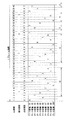
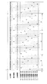
本発明の表示装置は、上記課題を解決するために、表示光源としての電流駆動型の電気光学素子と、電流制御端子と基準電位端子との間に印加される電圧により制御される出力電流を電流出力端子から上記電気光学素子に駆動電流として供給する駆動用トランジスタとが、マトリックス状に設けられた各画素に配置され、上記駆動電流が、データ配線から上記各画素に供給される、上記電気光学素子の点灯または消灯を示すデジタルの表示データに対応する表示装置において、上記駆動用トランジスタと第1スイッチ用トランジスタと上記電気光学素子とが直列に接続され、上記駆動用トランジスタの上記電流制御端子に第1コンデンサの一方端子が接続され、上記駆動用トランジスタの上記電流制御端子と上記電流出力端子との間に第2スイッチ用トランジスタが接続され、上記データ配線から上記各画素の上記表示データに対応する電位であって、上記表示データが点灯を示すものである場合には上記駆動用トランジスタをON状態とする電位が、また、上記表示データが消灯を示すものである場合には上記駆動用トランジスタをOFF状態とする電位が、上記駆動用トランジスタの上記電流制御端子に与えられて、上記第1コンデンサに、対応する電荷が保持された状態から始まる、あるいは、対応する電荷を保持する動作と同時に行われる第1期間において、上記第2スイッチ用トランジスタがON状態となり、上記第1スイッチ用トランジスタがOFF状態となり、第2期間において、上記第1コンデンサの他方端子の電位または、上記駆動用トランジスタの上記基準電位端子の電位が変化することにより、上記駆動用トランジスタの出力電流が設定されることを特徴としている。
Vs−Vth(min)<Vda ・・・(条件1)
であれば、駆動用トランジスタ(Q1)はその閾値電圧に依らずOFF状態となる。
Vs−Vth(max)>Vda ・・・(条件2)
であれば駆動用トランジスタはその閾値電圧に依らずON状態となる。
Vs−Vth(min)<Vda−Vx
であれば、駆動用トランジスタの電流制御端子の電位がVdaである駆動用トランジスタの出力状態をOFF状態のままとすることができる。
本実施の形態では、本発明の表示装置の第1の例について説明する。
VL<Vp−Vth(max)
VH>Vp−Vth(min)
とする。
VH−(Vcc−Vc)>Vp−Vth(min)
としておけば、状態VHの駆動用TFT:Q1はOFF状態のままとなる。一方、閾値補償期間に状態VLとなった場合の駆動用TFT:Q1のゲート電位は
Vp−Vth−(Vcc−Vc)
となり、駆動用TFT:Q1の閾値状態からVcc−Vcという一定電圧だけ低い電位となる。従って、駆動用TFT:Q1は、その閾値電圧Vthに依らず一定電流が流れる状態となる。
本実施の形態では、本発明の表示装置の第2の例について説明する。
VL<Vp−Vth(max)
VH>Vp−Vth(min)
とする。
VH−(Vcc−Vc)>Vp−Vth(min)
としておけば、状態VHの駆動用TFT:Q1はOFF状態のままとなる。一方、状態VLの駆動用TFT:Q1のゲート電位は
Vp−Vth−(Vcc−Vc)
となり、駆動用TFT:Q1の閾値電圧Vthに依らず駆動用TFT:Q1に一定電流が流れる状態となる。
本実施の形態では、本発明の表示装置の第3の例について説明する。
本実施の形態では、本発明の表示装置の第4の例について説明する。
Vp>Vda
の関係があれば、駆動用TFT:Q1のゲート・ソース間電圧Vdsの絶対値がVp−Vdaだけ大きくなるので、駆動用TFT:Q1はON状態となる。
Vp<Vda
であれば、駆動用TFT:Q1のゲート・ソース間電圧Vdsの絶対値がVda−Vpだけ小さくなるので、駆動用TFT:Q1はOFF状態となる。
本実施の形態では、本発明の表示装置の第5の例について説明する。
Vs<Vda
の関係がれば、駆動用TFT:Q1のゲート・ソース間電圧Vdsの絶対値が大きくなるので、駆動用TFT:Q1はON状態となる。
Vs>Vda
であれば、駆動用TFT:Q1のゲート・ソース間電圧Vdsの絶対値が小さくなるので、駆動用TFT:Q1はOFF状態となる。
本実施の形態では、本発明の表示装置の第6の例について説明する。
Vx>Vda
の関係があれば、駆動用TFT:Q1のゲート・ソース間電圧Vgsの絶対値が大きくなり、駆動用TFT:Q1はON状態となる。
Vx<Vda
であれば、駆動用TFT:Q1のゲート・ソース間電圧Vgsの絶対値が小さくなるので、駆動用TFT:Q1はOFF状態となる。
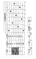
1/(60×320×8)≒6.5μs
以下に収める必要がある。ここで、「60」は1秒当たりのフレーム数、「320」は図9の320ライン、「8」は図4の1単位時間の占有時間数である。
Q2 スイッチ用TFT(第2スイッチ用トランジスタ)
Q3 スイッチ用TFT(第1スイッチ用トランジスタ)
Q4 スイッチ用TFT(第3スイッチ用トランジスタ)
Q5 スイッチ用TFT(第5スイッチ用トランジスタ)
Q6 駆動用TFT(駆動用トランジスタ)
Q7 スイッチ用TFT(第2スイッチ用トランジスタ)
Q8 スイッチ用TFT(第1スイッチ用トランジスタ)
Q9 スイッチ用TFT(第4スイッチ用トランジスタ)
Q11 スイッチ用TFT(第5スイッチ用トランジスタ)
Q12 スイッチ用TFT(第6スイッチ用トランジスタ)
Q13 スイッチ用TFT(第7スイッチ用トランジスタ)
Q14 スイッチ用TFT(第7スイッチ用トランジスタ)
Q15 スイッチ用TFT(第8スイッチ用トランジスタ)
C1 コンデンサ(第1コンデンサ)
C3 コンデンサ(第2コンデンサ)
C4 コンデンサ(第2コンデンサ)
C5 コンデンサ(第1コンデンサ)
C6 コンデンサ(第1コンデンサ)
C7 コンデンサ(第3コンデンサ)
EL1 有機EL(電気光学素子)
Dj データ配線
Ui 電位配線(第1配線)
Vp 電源配線
Vs 電位配線(第2配線)
Claims (14)
- 表示光源としての電流駆動型の電気光学素子と、電流制御端子と基準電位端子との間に印加される電圧により制御される出力電流を電流出力端子から上記電気光学素子に駆動電流として供給する駆動用トランジスタとが、マトリックス状に設けられた各画素に配置され、上記駆動電流が、データ配線から上記各画素に供給される、上記電気光学素子の点灯または消灯を示すデジタルの表示データに対応する表示装置において、
上記駆動用トランジスタと第1スイッチ用トランジスタと上記電気光学素子とが直列に接続され、
上記駆動用トランジスタの上記電流制御端子に第1コンデンサの一方端子が接続され、
上記駆動用トランジスタの上記電流制御端子と上記電流出力端子との間に第2スイッチ用トランジスタが接続され、
上記第2スイッチ用トランジスタがON状態であるとともに上記第1スイッチ用トランジスタがOFF状態であり、上記データ配線から上記各画素の上記表示データに対応する電位であって、上記表示データが点灯を示すものである場合には上記駆動用トランジスタをON状態とする電位が、また、上記表示データが消灯を示すものである場合には上記駆動用トランジスタをOFF状態とする電位が、上記駆動用トランジスタの上記電流制御端子に伝達される表示データ付与期間と、
上記表示データ付与期間の後に続く第1期間であって、上記第2スイッチ用トランジスタがON状態であるとともに上記第1スイッチ用トランジスタがOFF状態であり、上記データ配線から上記電流制御端子への上記電位の伝達が遮断される第1期間とを経る動作を行い、
上記動作を行った後の第2期間において、上記第1コンデンサの他方端子の電位または、上記駆動用トランジスタの上記基準電位端子の電位が変化することにより、上記駆動用トランジスタの出力電流が設定されることを特徴とする表示装置。 - 上記第1コンデンサの上記他方端子は第1配線に接続されていることを特徴とする請求項1に記載の表示装置。
- 上記第2期間に上記第1配線の電位が変化して、上記駆動用トランジスタがOFF状態からON状態に変化する、または、OFF状態を維持することにより、上記駆動電流の有無が決定されることを特徴とする請求項2に記載の表示装置。
- 上記駆動用トランジスタの上記電流出力端子と上記データ配線との間に第3スイッチ用トランジスタが接続されていることを特徴とする請求項1から3までのいずれか1項に記載の表示装置。
- 上記表示データ付与期間に上記第3スイッチ用トランジスタがON状態となることを特徴とする請求項4に記載の表示装置。
- 上記駆動用トランジスタの上記電流制御端子と上記データ配線との間に第4スイッチ用トランジスタが接続されていることを特徴とする請求項1から3までのいずれか1項に記載の表示装置。
- 上記駆動用トランジスタの上記電流出力端子と上記データ配線とは第2コンデンサを介して接続されていることを特徴とする請求項1から3までのいずれか1項に記載の表示装置。
- 上記駆動用トランジスタの上記基準電位端子と上記データ配線との間に第5スイッチ用トランジスタが接続され、
上記駆動用トランジスタの上記基準電位端子と、上記駆動用トランジスタの出力電流を生成する電源の電位を与える電源配線との間に、第6スイッチ用トランジスタが接続されていることを特徴とする請求項1に記載の表示装置。 - 上記第1コンデンサの上記他方端子と、上記駆動用トランジスタの出力電流を生成する電源の電位を与える電源配線との間に、第3コンデンサが接続され、
上記第1コンデンサの上記他方端子と上記データ配線との間に第7スイッチ用トランジスタが接続されていることを特徴とする請求項1に記載の表示装置。 - 上記第1コンデンサの上記他方端子と所定の電位を与える第2配線との間に第8スイッチ用トランジスタが接続され、
上記第1コンデンサの上記他方端子と上記データ配線との間に第7スイッチ用トランジスタが接続されていることを特徴とする請求項1に記載の表示装置。 - 表示光源としての電流駆動型の電気光学素子と、電流制御端子と基準電位端子との間に印加される電圧により制御される出力電流を電流出力端子から上記電気光学素子に駆動電流として供給する駆動用トランジスタとが、マトリックス状に設けられた各画素に配置され、上記駆動電流が、データ配線から上記各画素に供給される、上記電気光学素子の点灯または消灯を示すデジタルの表示データに対応する表示装置において、
上記駆動用トランジスタと第1スイッチ用トランジスタと上記電気光学素子とが直列に接続され、
上記駆動用トランジスタの上記電流制御端子に第1コンデンサの一方端子が接続され、
上記駆動用トランジスタの上記電流制御端子と上記電流出力端子との間に第2スイッチ用トランジスタが接続され、
上記駆動用トランジスタの上記電流制御端子と上記データ配線との間に第4スイッチ用トランジスタが接続され、
上記データ配線から上記各画素の上記表示データに対応する電位であって、上記表示データが点灯を示すものである場合には上記駆動用トランジスタをON状態とする電位が、また、上記表示データが消灯を示すものである場合には上記駆動用トランジスタをOFF状態とする電位が、上記駆動用トランジスタの上記電流制御端子に与えられて、上記第1コンデンサに、対応する電荷が保持された状態から始まる、あるいは、対応する電荷を保持する動作と同時に行われる第1期間において、上記第2スイッチ用トランジスタがON状態となり、上記第1スイッチ用トランジスタがOFF状態となり、
第2期間において、上記第1コンデンサの他方端子の電位または、上記駆動用トランジスタの上記基準電位端子の電位が変化することにより、上記駆動用トランジスタの出力電流が設定されることを特徴とする表示装置。 - 表示光源としての電流駆動型の電気光学素子と、電流制御端子と基準電位端子との間に印加される電圧により制御される出力電流を電流出力端子から上記電気光学素子に駆動電流として供給する駆動用トランジスタとが、マトリックス状に設けられた各画素に配置され、上記駆動電流が、データ配線から上記各画素に供給される、上記電気光学素子の点灯または消灯を示すデジタルの表示データに対応する表示装置において、
上記駆動用トランジスタと第1スイッチ用トランジスタと上記電気光学素子とが直列に接続され、
上記駆動用トランジスタの上記電流制御端子に第1コンデンサの一方端子が接続され、
上記駆動用トランジスタの上記電流制御端子と上記電流出力端子との間に第2スイッチ用トランジスタが接続され、
上記駆動用トランジスタの上記電流出力端子と上記データ配線とは第2コンデンサを介して接続され、
上記データ配線から上記各画素の上記表示データに対応する電位であって、上記表示データが点灯を示すものである場合には上記駆動用トランジスタをON状態とする電位が、また、上記表示データが消灯を示すものである場合には上記駆動用トランジスタをOFF状態とする電位が、上記駆動用トランジスタの上記電流制御端子に与えられて、上記第1コンデンサに、対応する電荷が保持された状態から始まる、あるいは、対応する電荷を保持する動作と同時に行われる第1期間において、上記第2スイッチ用トランジスタがON状態となり、上記第1スイッチ用トランジスタがOFF状態となり、
第2期間において、上記第1コンデンサの他方端子の電位または、上記駆動用トランジスタの上記基準電位端子の電位が変化することにより、上記駆動用トランジスタの出力電流が設定されることを特徴とする表示装置。 - 上記第1コンデンサの上記他方端子は第1配線に接続されていることを特徴とする請求項11または12に記載の表示装置。
- 表示光源としての電流駆動型の電気光学素子と、電流制御端子と基準電位端子との間に印加される電圧により制御される出力電流を電流出力端子から上記電気光学素子に駆動電流として供給する駆動用トランジスタとが、マトリックス状に設けられた各画素に配置され、上記駆動電流が、データ配線から上記各画素に供給される、上記電気光学素子の点灯または消灯を示すデジタルの表示データに対応する表示装置において、
上記駆動用トランジスタと第1スイッチ用トランジスタと上記電気光学素子とが直列に接続され、
上記駆動用トランジスタの上記電流制御端子に第1コンデンサの一方端子が接続され、
上記駆動用トランジスタの上記電流制御端子と上記電流出力端子との間に第2スイッチ用トランジスタが接続された表示装置の駆動方法であって、
上記第2スイッチ用トランジスタがON状態であるとともに上記第1スイッチ用トランジスタがOFF状態であり、上記データ配線から上記各画素の上記表示データに対応する電位であって、上記表示データが点灯を示すものである場合には上記駆動用トランジスタをON状態とする電位が、また、上記表示データが消灯を示すものである場合には上記駆動用トランジスタをOFF状態とする電位が、上記駆動用トランジスタの上記電流制御端子に伝達される表示データ付与期間と、
上記表示データ付与期間の後に続く第1期間であって、上記第2スイッチ用トランジスタがON状態であるとともに上記第1スイッチ用トランジスタがOFF状態であり、上記データ配線から上記電流制御端子への上記電位の伝達が遮断される第1期間とを経る動作を行い、
上記動作を行った後の第2期間において、上記第1コンデンサの他方端子の電位または、上記駆動用トランジスタの上記基準電位端子電位を変化させることにより、上記駆動用トランジスタの出力電流を設定することを特徴とする表示装置の駆動方法。
Priority Applications (2)
| Application Number | Priority Date | Filing Date | Title |
|---|---|---|---|
| JP2004254615A JP4160032B2 (ja) | 2004-09-01 | 2004-09-01 | 表示装置およびその駆動方法 |
| US11/184,003 US7443367B2 (en) | 2004-09-01 | 2005-07-19 | Display device and method for driving the same |
Applications Claiming Priority (1)
| Application Number | Priority Date | Filing Date | Title |
|---|---|---|---|
| JP2004254615A JP4160032B2 (ja) | 2004-09-01 | 2004-09-01 | 表示装置およびその駆動方法 |
Publications (2)
| Publication Number | Publication Date |
|---|---|
| JP2006071919A JP2006071919A (ja) | 2006-03-16 |
| JP4160032B2 true JP4160032B2 (ja) | 2008-10-01 |
Family
ID=35942362
Family Applications (1)
| Application Number | Title | Priority Date | Filing Date |
|---|---|---|---|
| JP2004254615A Expired - Fee Related JP4160032B2 (ja) | 2004-09-01 | 2004-09-01 | 表示装置およびその駆動方法 |
Country Status (2)
| Country | Link |
|---|---|
| US (1) | US7443367B2 (ja) |
| JP (1) | JP4160032B2 (ja) |
Families Citing this family (38)
| Publication number | Priority date | Publication date | Assignee | Title |
|---|---|---|---|---|
| EP1627372A1 (en) * | 2003-05-02 | 2006-02-22 | Koninklijke Philips Electronics N.V. | Active matrix oled display device with threshold voltage drift compensation |
| JP4327042B2 (ja) * | 2004-08-05 | 2009-09-09 | シャープ株式会社 | 表示装置およびその駆動方法 |
| US20080136795A1 (en) * | 2005-03-25 | 2008-06-12 | Takaji Numao | Display Device and Driving Method Thereof |
| DE102005016866A1 (de) * | 2005-04-12 | 2006-10-19 | Siemens Ag | Verfahren sowie Vorrichtung zum Synchronisieren von inhaltsbezogenen ersten Datensegmenten einer ersten Datendatei und inhaltsbezogenen zweiten Datensegmenten einer zweiten Datendatei |
| JP2006317696A (ja) * | 2005-05-12 | 2006-11-24 | Sony Corp | 画素回路および表示装置、並びに画素回路の制御方法 |
| JP2006349794A (ja) * | 2005-06-14 | 2006-12-28 | Seiko Epson Corp | 電子回路、その駆動方法、電気光学装置および電子機器 |
| WO2007063814A1 (en) * | 2005-12-02 | 2007-06-07 | Semiconductor Energy Laboratory Co., Ltd. | Semiconductor device, display device, and electronic device |
| EP1793366A3 (en) | 2005-12-02 | 2009-11-04 | Semiconductor Energy Laboratory Co., Ltd. | Semiconductor device, display device, and electronic device |
| JP2008192642A (ja) * | 2007-01-31 | 2008-08-21 | Tokyo Electron Ltd | 基板処理装置 |
| KR101526475B1 (ko) | 2007-06-29 | 2015-06-05 | 가부시키가이샤 한도오따이 에네루기 켄큐쇼 | 표시 장치 및 그 구동 방법 |
| JP2009276744A (ja) * | 2008-02-13 | 2009-11-26 | Toshiba Mobile Display Co Ltd | El表示装置 |
| JP2009237041A (ja) * | 2008-03-26 | 2009-10-15 | Sony Corp | 画像表示装置及び画像表示方法 |
| KR101057699B1 (ko) * | 2008-05-15 | 2011-08-19 | 매그나칩 반도체 유한회사 | 원-타임 프로그래머블 기능을 갖는 메모리 장치, 이를구비한 표시패널 구동 칩 및 표시장치 |
| JP5736114B2 (ja) | 2009-02-27 | 2015-06-17 | 株式会社半導体エネルギー研究所 | 半導体装置の駆動方法、電子機器の駆動方法 |
| US9047815B2 (en) * | 2009-02-27 | 2015-06-02 | Semiconductor Energy Laboratory Co., Ltd. | Method for driving semiconductor device |
| TWI416536B (zh) * | 2009-07-21 | 2013-11-21 | Novatek Microelectronics Corp | 多晶片設定位址的方法與結構以及應用的顯示系統 |
| JP2011107692A (ja) | 2009-10-20 | 2011-06-02 | Semiconductor Energy Lab Co Ltd | 表示装置の駆動方法、表示装置、及び電子機器。 |
| KR20120065139A (ko) * | 2010-12-10 | 2012-06-20 | 삼성모바일디스플레이주식회사 | 표시 장치를 위한 화소, 이를 이용한 표시 장치 및 그 구동 방법 |
| KR102378948B1 (ko) | 2011-07-22 | 2022-03-24 | 가부시키가이샤 한도오따이 에네루기 켄큐쇼 | 발광 장치 |
| KR102263816B1 (ko) * | 2011-10-18 | 2021-06-14 | 가부시키가이샤 한도오따이 에네루기 켄큐쇼 | 발광 장치 |
| US12176356B2 (en) | 2011-10-18 | 2024-12-24 | Semiconductor Energy Laboratory Co., Ltd. | Semiconductor device including transistor and light-emitting element |
| US10043794B2 (en) | 2012-03-22 | 2018-08-07 | Semiconductor Energy Laboratory Co., Ltd. | Semiconductor device and electronic device |
| TWI587261B (zh) | 2012-06-01 | 2017-06-11 | 半導體能源研究所股份有限公司 | 半導體裝置及半導體裝置的驅動方法 |
| JP6228753B2 (ja) | 2012-06-01 | 2017-11-08 | 株式会社半導体エネルギー研究所 | 半導体装置、表示装置、表示モジュール、及び電子機器 |
| KR20140065937A (ko) * | 2012-11-22 | 2014-05-30 | 삼성디스플레이 주식회사 | 유기전계발광 표시장치 |
| JP5910543B2 (ja) * | 2013-03-06 | 2016-04-27 | ソニー株式会社 | 表示装置、表示駆動回路、表示駆動方法、および電子機器 |
| WO2015097595A1 (en) | 2013-12-27 | 2015-07-02 | Semiconductor Energy Laboratory Co., Ltd. | Light-emitting device |
| CN104680976B (zh) * | 2015-02-09 | 2017-02-22 | 京东方科技集团股份有限公司 | 像素补偿电路、显示装置及驱动方法 |
| KR102485572B1 (ko) * | 2016-05-18 | 2023-01-09 | 삼성디스플레이 주식회사 | 표시 장치 및 이의 구동 방법 |
| KR102621655B1 (ko) * | 2017-01-09 | 2024-01-09 | 삼성디스플레이 주식회사 | 화소 및 이를 이용한 유기전계발광 표시장치 |
| KR102583838B1 (ko) * | 2017-01-17 | 2023-10-05 | 삼성디스플레이 주식회사 | 화소 및 이를 이용한 유기전계발광 표시장치 |
| KR102575662B1 (ko) * | 2017-02-06 | 2023-09-07 | 삼성디스플레이 주식회사 | 화소 및 이를 포함하는 표시 장치 |
| KR102660207B1 (ko) * | 2017-02-09 | 2024-04-25 | 삼성디스플레이 주식회사 | 화소 및 이를 포함하는 표시 장치 |
| CN107507566B (zh) * | 2017-10-13 | 2019-09-10 | 京东方科技集团股份有限公司 | 像素驱动电路、显示装置和驱动方法 |
| KR102498274B1 (ko) * | 2017-12-06 | 2023-02-10 | 삼성디스플레이 주식회사 | 표시 장치 및 이의 구동 방법 |
| CN110189705B (zh) * | 2019-06-19 | 2021-02-05 | 京东方科技集团股份有限公司 | 像素电路、显示面板和显示设备 |
| KR102657133B1 (ko) | 2019-07-22 | 2024-04-16 | 삼성디스플레이 주식회사 | 화소 및 이를 포함하는 표시 장치 |
| EP4651686A3 (en) | 2020-01-28 | 2026-02-25 | OLEDWorks LLC | Stacked oled microdisplay with low-voltage silicon backplane |
Family Cites Families (12)
| Publication number | Priority date | Publication date | Assignee | Title |
|---|---|---|---|---|
| JP3834086B2 (ja) | 1995-11-06 | 2006-10-18 | シャープ株式会社 | マトリックス型表示装置およびその駆動方法 |
| KR20050084509A (ko) | 1997-04-23 | 2005-08-26 | 사르노프 코포레이션 | 능동 매트릭스 발광 다이오드 화소 구조물 및 이를동작시키는 방법 |
| GB0008019D0 (en) | 2000-03-31 | 2000-05-17 | Koninkl Philips Electronics Nv | Display device having current-addressed pixels |
| US7365713B2 (en) * | 2001-10-24 | 2008-04-29 | Semiconductor Energy Laboratory Co., Ltd. | Semiconductor device and driving method thereof |
| JP4030863B2 (ja) | 2002-04-09 | 2008-01-09 | シャープ株式会社 | 電気光学装置、それを用いた表示装置、その駆動方法、並びに、その重みの設定方法 |
| JP4416456B2 (ja) * | 2002-09-02 | 2010-02-17 | キヤノン株式会社 | エレクトロルミネッセンス装置 |
| JP4467909B2 (ja) * | 2002-10-04 | 2010-05-26 | シャープ株式会社 | 表示装置 |
| JP3832415B2 (ja) | 2002-10-11 | 2006-10-11 | ソニー株式会社 | アクティブマトリクス型表示装置 |
| KR100490622B1 (ko) | 2003-01-21 | 2005-05-17 | 삼성에스디아이 주식회사 | 유기 전계발광 표시장치 및 그 구동방법과 픽셀회로 |
| JP2004341351A (ja) | 2003-05-16 | 2004-12-02 | Toshiba Matsushita Display Technology Co Ltd | アクティブマトリクス型表示装置 |
| KR100560780B1 (ko) | 2003-07-07 | 2006-03-13 | 삼성에스디아이 주식회사 | 유기전계 발광표시장치의 화소회로 및 그의 구동방법 |
| TW200504662A (en) * | 2003-07-17 | 2005-02-01 | Analog Integrations Corp | Method of using current mirror to drive LED |
-
2004
- 2004-09-01 JP JP2004254615A patent/JP4160032B2/ja not_active Expired - Fee Related
-
2005
- 2005-07-19 US US11/184,003 patent/US7443367B2/en active Active
Also Published As
| Publication number | Publication date |
|---|---|
| US20060044244A1 (en) | 2006-03-02 |
| JP2006071919A (ja) | 2006-03-16 |
| US7443367B2 (en) | 2008-10-28 |
Similar Documents
| Publication | Publication Date | Title |
|---|---|---|
| JP2006071919A (ja) | 表示装置およびその駆動方法 | |
| JP6675446B2 (ja) | 表示装置 | |
| CN112313732B (zh) | 显示设备 | |
| KR100914186B1 (ko) | 신호선 구동회로, 발광장치 및 그 구동방법 | |
| KR101404547B1 (ko) | 표시 장치 및 그 구동 방법 | |
| CN101536070B (zh) | 像素电路及显示装置 | |
| US20100073344A1 (en) | Pixel circuit and display device | |
| KR100667664B1 (ko) | 화소 회로의 구동 방법, 화소 회로 및 전자 기기 | |
| CN101221725B (zh) | 显示装置及其驱动方法 | |
| TWI537922B (zh) | Display device | |
| KR20050042041A (ko) | 신호선 구동회로 및 발광장치 | |
| JP2005099712A (ja) | 表示装置の駆動回路および表示装置 | |
| US8810488B2 (en) | Display device and method for driving the same | |
| KR20040107047A (ko) | 유기전계발광 구동소자와, 이를 갖는 표시패널 및 표시장치 | |
| WO2006103797A1 (ja) | 表示装置およびその駆動方法 | |
| KR102625961B1 (ko) | 전계 발광 표시장치 | |
| US20060214889A1 (en) | Active matrix type display device | |
| WO2006103802A1 (ja) | 表示装置及びその駆動方法 | |
| KR101552991B1 (ko) | 유기 발광 다이오드 표시장치의 구동장치와 그 구동방법 | |
| CN120183338A (zh) | 栅极驱动电路以及包括该栅极驱动电路的显示装置 | |
| JP4788819B2 (ja) | 電気光学装置および電子機器 | |
| JP4780121B2 (ja) | 表示駆動装置、表示装置及びその表示駆動方法 | |
| JP2006138953A (ja) | 表示装置およびその駆動方法 | |
| KR20210040727A (ko) | 표시장치와 그 구동 방법 | |
| KR20260050810A (ko) | 표시장치와 그 구동방법 |
Legal Events
| Date | Code | Title | Description |
|---|---|---|---|
| A977 | Report on retrieval |
Free format text: JAPANESE INTERMEDIATE CODE: A971007 Effective date: 20071225 |
|
| A131 | Notification of reasons for refusal |
Free format text: JAPANESE INTERMEDIATE CODE: A131 Effective date: 20080108 |
|
| A521 | Request for written amendment filed |
Free format text: JAPANESE INTERMEDIATE CODE: A523 Effective date: 20080303 |
|
| A131 | Notification of reasons for refusal |
Free format text: JAPANESE INTERMEDIATE CODE: A131 Effective date: 20080507 |
|
| A521 | Request for written amendment filed |
Free format text: JAPANESE INTERMEDIATE CODE: A523 Effective date: 20080616 |
|
| TRDD | Decision of grant or rejection written | ||
| A01 | Written decision to grant a patent or to grant a registration (utility model) |
Free format text: JAPANESE INTERMEDIATE CODE: A01 Effective date: 20080715 |
|
| A01 | Written decision to grant a patent or to grant a registration (utility model) |
Free format text: JAPANESE INTERMEDIATE CODE: A01 |
|
| A61 | First payment of annual fees (during grant procedure) |
Free format text: JAPANESE INTERMEDIATE CODE: A61 Effective date: 20080716 |
|
| R150 | Certificate of patent or registration of utility model |
Free format text: JAPANESE INTERMEDIATE CODE: R150 Ref document number: 4160032 Country of ref document: JP Free format text: JAPANESE INTERMEDIATE CODE: R150 |
|
| FPAY | Renewal fee payment (event date is renewal date of database) |
Free format text: PAYMENT UNTIL: 20110725 Year of fee payment: 3 |
|
| FPAY | Renewal fee payment (event date is renewal date of database) |
Free format text: PAYMENT UNTIL: 20110725 Year of fee payment: 3 |
|
| FPAY | Renewal fee payment (event date is renewal date of database) |
Free format text: PAYMENT UNTIL: 20120725 Year of fee payment: 4 |
|
| FPAY | Renewal fee payment (event date is renewal date of database) |
Free format text: PAYMENT UNTIL: 20120725 Year of fee payment: 4 |
|
| FPAY | Renewal fee payment (event date is renewal date of database) |
Free format text: PAYMENT UNTIL: 20130725 Year of fee payment: 5 |
|
| LAPS | Cancellation because of no payment of annual fees |