JP4162560B2 - 窒化物系半導体発光素子 - Google Patents
窒化物系半導体発光素子 Download PDFInfo
- Publication number
- JP4162560B2 JP4162560B2 JP2003319528A JP2003319528A JP4162560B2 JP 4162560 B2 JP4162560 B2 JP 4162560B2 JP 2003319528 A JP2003319528 A JP 2003319528A JP 2003319528 A JP2003319528 A JP 2003319528A JP 4162560 B2 JP4162560 B2 JP 4162560B2
- Authority
- JP
- Japan
- Prior art keywords
- layer
- nitride
- undoped
- type
- based semiconductor
- Prior art date
- Legal status (The legal status is an assumption and is not a legal conclusion. Google has not performed a legal analysis and makes no representation as to the accuracy of the status listed.)
- Expired - Fee Related
Links
- 239000004065 semiconductor Substances 0.000 title claims description 241
- 150000004767 nitrides Chemical class 0.000 title claims description 231
- 239000000758 substrate Substances 0.000 claims description 53
- 229910002704 AlGaN Inorganic materials 0.000 claims description 8
- 239000010410 layer Substances 0.000 description 525
- 238000005253 cladding Methods 0.000 description 67
- 230000031700 light absorption Effects 0.000 description 38
- 239000012535 impurity Substances 0.000 description 33
- 239000013078 crystal Substances 0.000 description 29
- 230000007547 defect Effects 0.000 description 20
- 238000004519 manufacturing process Methods 0.000 description 20
- 239000011241 protective layer Substances 0.000 description 20
- JMASRVWKEDWRBT-UHFFFAOYSA-N Gallium nitride Chemical compound [Ga]#N JMASRVWKEDWRBT-UHFFFAOYSA-N 0.000 description 18
- 239000007789 gas Substances 0.000 description 17
- 238000000034 method Methods 0.000 description 17
- 229910052594 sapphire Inorganic materials 0.000 description 15
- 239000010980 sapphire Substances 0.000 description 15
- 239000012159 carrier gas Substances 0.000 description 13
- 230000004888 barrier function Effects 0.000 description 10
- 230000000694 effects Effects 0.000 description 9
- XCZXGTMEAKBVPV-UHFFFAOYSA-N trimethylgallium Chemical compound C[Ga](C)C XCZXGTMEAKBVPV-UHFFFAOYSA-N 0.000 description 8
- 239000000203 mixture Substances 0.000 description 7
- 239000002019 doping agent Substances 0.000 description 5
- RGGPNXQUMRMPRA-UHFFFAOYSA-N triethylgallium Chemical compound CC[Ga](CC)CC RGGPNXQUMRMPRA-UHFFFAOYSA-N 0.000 description 5
- IBEFSUTVZWZJEL-UHFFFAOYSA-N trimethylindium Chemical compound C[In](C)C IBEFSUTVZWZJEL-UHFFFAOYSA-N 0.000 description 5
- QVGXLLKOCUKJST-UHFFFAOYSA-N atomic oxygen Chemical compound [O] QVGXLLKOCUKJST-UHFFFAOYSA-N 0.000 description 4
- 239000000463 material Substances 0.000 description 4
- 238000002488 metal-organic chemical vapour deposition Methods 0.000 description 4
- 230000004048 modification Effects 0.000 description 4
- 238000012986 modification Methods 0.000 description 4
- 229910052760 oxygen Inorganic materials 0.000 description 4
- 239000001301 oxygen Substances 0.000 description 4
- 238000001771 vacuum deposition Methods 0.000 description 4
- 238000005530 etching Methods 0.000 description 3
- 238000010884 ion-beam technique Methods 0.000 description 3
- 239000002994 raw material Substances 0.000 description 3
- 239000000969 carrier Substances 0.000 description 2
- 230000002542 deteriorative effect Effects 0.000 description 2
- 229910052738 indium Inorganic materials 0.000 description 2
- 238000001459 lithography Methods 0.000 description 2
- 230000003287 optical effect Effects 0.000 description 2
- 238000005268 plasma chemical vapour deposition Methods 0.000 description 2
- 238000005498 polishing Methods 0.000 description 2
- 238000000926 separation method Methods 0.000 description 2
- MHYQBXJRURFKIN-UHFFFAOYSA-N C1(C=CC=C1)[Mg] Chemical compound C1(C=CC=C1)[Mg] MHYQBXJRURFKIN-UHFFFAOYSA-N 0.000 description 1
- 229910001218 Gallium arsenide Inorganic materials 0.000 description 1
- 229910004298 SiO 2 Inorganic materials 0.000 description 1
- 230000004913 activation Effects 0.000 description 1
- 238000005229 chemical vapour deposition Methods 0.000 description 1
- 238000004891 communication Methods 0.000 description 1
- 230000006866 deterioration Effects 0.000 description 1
- 230000002349 favourable effect Effects 0.000 description 1
- 238000010438 heat treatment Methods 0.000 description 1
- 125000005842 heteroatom Chemical group 0.000 description 1
- 238000002347 injection Methods 0.000 description 1
- 239000007924 injection Substances 0.000 description 1
- 229910052751 metal Inorganic materials 0.000 description 1
- 239000002184 metal Substances 0.000 description 1
- 239000010453 quartz Substances 0.000 description 1
- 230000006798 recombination Effects 0.000 description 1
- 238000005215 recombination Methods 0.000 description 1
- 239000011347 resin Substances 0.000 description 1
- 229920005989 resin Polymers 0.000 description 1
- VYPSYNLAJGMNEJ-UHFFFAOYSA-N silicon dioxide Inorganic materials O=[Si]=O VYPSYNLAJGMNEJ-UHFFFAOYSA-N 0.000 description 1
- 239000002356 single layer Substances 0.000 description 1
- 239000011029 spinel Substances 0.000 description 1
- 229910052596 spinel Inorganic materials 0.000 description 1
- 239000010421 standard material Substances 0.000 description 1
- JLTRXTDYQLMHGR-UHFFFAOYSA-N trimethylaluminium Chemical compound C[Al](C)C JLTRXTDYQLMHGR-UHFFFAOYSA-N 0.000 description 1
- 238000007738 vacuum evaporation Methods 0.000 description 1
- 238000000927 vapour-phase epitaxy Methods 0.000 description 1
Images




Landscapes
- Semiconductor Lasers (AREA)
- Led Devices (AREA)
Description
「電子情報通信学会技術研究報告」電子情報通信学会、2002年6月15日、pp.63−66
図1は、本発明の第1実施形態による窒化物系半導体発光ダイオード素子(青色LEDチップ)を示した断面図であり、図2は、図1に示した第1実施形態による窒化物系半導体発光ダイオード素子の上面図である。まず、図1および図2を参照して、第1実施形態による窒化物系半導体発光ダイオード素子の構造について説明する。
また、アンドープコンタクト層8の上面上には、下から上に向かって、約100nmの膜厚を有するPd膜と、約100nmの膜厚を有するAu膜とから構成されるくし状のp側電極9が形成されている。なお、p側電極9は、本発明の「電極」の一例である。
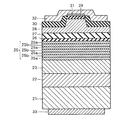
図6は、本発明の第2実施形態による窒化物系半導体レーザ素子(LDチップ)を示した断面図である。図6を参照して、この第2実施形態では、窒化物系半導体発光ダイオード素子に本発明を適用した第1実施形態と異なり、窒化物系半導体レーザ素子に本発明を適用した例について説明する。
図10は、本発明の第3実施形態による窒化物系半導体発光ダイオード素子(青色LEDチップ)を示した断面図である。図10を参照して、この第3実施形態では、上記第1実施形態において形成された高温バッファ層3に代えて、より低転位のアンドープGaN層44を形成した例について説明する。なお、その他の構成は、第1実施形態と同様である。
図14は、本発明の第4実施形態による窒化物系半導体レーザ素子(LDチップ)を示した断面図である。図14を参照して、この第4実施形態では、上記第2実施形態において形成されたn型光ガイド層24を設けない例について説明する。なお、その他の構成は、第2実施形態と同様である。
4 n型コンタクト層(第1窒化物系半導体層)
5、25 MQW活性層(活性層)
7、28 p型クラッド層(第2窒化物系半導体層、クラッド層)
8、29、59 アンドープコンタクト層
9、31 p側電極(電極)
21 n型GaN基板(基板)
22 n型GaN層(第1窒化物系半導体層)
23 n型クラッド層(第1窒化物系半導体層)
24、64 n型光ガイド層
27 光ガイド層(第3窒化物系半導体層)
49 p側コンタクト層(アンドープコンタクト層)
Claims (11)
- 基板上に形成された第1導電型の第1窒化物系半導体層と、
前記第1窒化物系半導体層上に形成され、窒化物系半導体層からなる活性層と、
前記活性層上に形成された第2導電型の第2窒化物系半導体層と、
前記第2窒化物系半導体層上に形成された窒化物系半導体からなるアンドープコンタクト層と、
前記アンドープコンタクト層上に形成された電極とを備えた、窒化物系半導体発光素子であって、
前記アンドープコンタクト層は、InGaNを含む、窒化物系半導体発光素子。 - 前記アンドープコンタクト層のバンドギャップは、前記第2窒化物系半導体層のバンドギャップよりも小さい、請求項1に記載の窒化物系半導体発光素子。
- 前記第1導電型の第1窒化物系半導体層は、n型の第1窒化物系半導体層であり、
前記第2導電型の第2窒化物系半導体層は、p型の第2窒化物系半導体層である、請求項1または2に記載の窒化物系半導体発光素子。 - 前記第2導電型の第2窒化物系半導体層は、AlGaNを含む、請求項1〜3のいずれか1項に記載の窒化物系半導体発光素子。
- 前記アンドープコンタクト層は、1nm以上10nm以下の厚みを有する、請求項1〜4のいずれか1項に記載の窒化物系半導体発光素子。
- 前記アンドープコンタクト層は、前記活性層のバンドギャップよりも大きいバンドギャップを有する、請求項1〜5のいずれか1項に記載の窒化物系半導体発光素子。
- 前記アンドープコンタクト層は、単一のアンドープの窒化物系半導体層により構成されている、請求項1〜6のいずれか1項に記載の窒化物系半導体発光素子。
- 前記アンドープコンタクト層の上面上に、Pd膜を含む電極を備えている、請求項1〜7のいずれか1項に記載の窒化物系半導体発光素子。
- 少なくとも前記活性層と前記第2導電型の第2窒化物系半導体層との間に形成され、前記第2窒化物系半導体層よりもバンドギャップの小さい窒化物系半導体からなるアンドープの第3窒化物系半導体層をさらに備える、請求項1〜8のいずれか1項に記載の窒化物系半導体発光素子。
- 前記アンドープの第3窒化物系半導体層は、前記活性層と、前記第1導電型の第1窒化物系半導体層および前記第2導電型の第2窒化物系半導体層との間のうち、前記活性層と前記第2窒化物系半導体層との間にのみ形成されている、請求項9に記載の窒化物系半導体発光素子。
- 前記活性層と前記第1導電型の第1窒化物系半導体層との間に形成された第4窒化物系半導体層をさらに備え、
前記第4窒化物系半導体層は、前記第3窒化物系半導体層の膜厚よりも小さい膜厚を有する、請求項9〜10のいずれか1項に記載の窒化物系半導体発光素子。
Priority Applications (1)
| Application Number | Priority Date | Filing Date | Title |
|---|---|---|---|
| JP2003319528A JP4162560B2 (ja) | 2002-09-18 | 2003-09-11 | 窒化物系半導体発光素子 |
Applications Claiming Priority (2)
| Application Number | Priority Date | Filing Date | Title |
|---|---|---|---|
| JP2002271968 | 2002-09-18 | ||
| JP2003319528A JP4162560B2 (ja) | 2002-09-18 | 2003-09-11 | 窒化物系半導体発光素子 |
Related Child Applications (1)
| Application Number | Title | Priority Date | Filing Date |
|---|---|---|---|
| JP2008109596A Division JP5036617B2 (ja) | 2002-09-18 | 2008-04-18 | 窒化物系半導体発光素子 |
Publications (2)
| Publication Number | Publication Date |
|---|---|
| JP2004134772A JP2004134772A (ja) | 2004-04-30 |
| JP4162560B2 true JP4162560B2 (ja) | 2008-10-08 |
Family
ID=32301696
Family Applications (1)
| Application Number | Title | Priority Date | Filing Date |
|---|---|---|---|
| JP2003319528A Expired - Fee Related JP4162560B2 (ja) | 2002-09-18 | 2003-09-11 | 窒化物系半導体発光素子 |
Country Status (1)
| Country | Link |
|---|---|
| JP (1) | JP4162560B2 (ja) |
Families Citing this family (12)
| Publication number | Priority date | Publication date | Assignee | Title |
|---|---|---|---|---|
| KR100568502B1 (ko) * | 2004-08-11 | 2006-04-07 | 한국전자통신연구원 | 반도체 발광소자 |
| JP2006100475A (ja) * | 2004-09-29 | 2006-04-13 | Toyoda Gosei Co Ltd | 半導体発光素子 |
| JP4967243B2 (ja) * | 2005-03-08 | 2012-07-04 | 三菱化学株式会社 | GaN系発光ダイオードおよび発光装置 |
| JP4956902B2 (ja) * | 2005-03-18 | 2012-06-20 | 三菱化学株式会社 | GaN系発光ダイオードおよびそれを用いた発光装置 |
| KR100588377B1 (ko) | 2005-05-10 | 2006-06-09 | 삼성전기주식회사 | 수직구조 질화갈륨계 발광다이오드 소자 및 그 제조방법 |
| EP2034524A1 (en) * | 2006-05-26 | 2009-03-11 | Rohm Co., Ltd. | Nitride semiconductor light emitting element |
| WO2007138657A1 (ja) * | 2006-05-26 | 2007-12-06 | Rohm Co., Ltd. | 窒化物半導体発光素子 |
| JP5321656B2 (ja) * | 2011-08-05 | 2013-10-23 | 三菱化学株式会社 | GaN系発光ダイオードおよび発光装置 |
| JP5304855B2 (ja) * | 2011-08-12 | 2013-10-02 | 三菱化学株式会社 | GaN系発光ダイオードおよびそれを用いた発光装置 |
| JP5733295B2 (ja) * | 2012-12-04 | 2015-06-10 | 住友電気工業株式会社 | 窒化物半導体発光素子、窒化物半導体発光素子を作製する方法 |
| WO2016006298A1 (ja) * | 2014-07-07 | 2016-01-14 | ソニー株式会社 | 半導体光デバイス |
| JP2021150373A (ja) * | 2020-03-17 | 2021-09-27 | セイコーエプソン株式会社 | 発光装置、プロジェクター、およびディスプレイ |
-
2003
- 2003-09-11 JP JP2003319528A patent/JP4162560B2/ja not_active Expired - Fee Related
Also Published As
| Publication number | Publication date |
|---|---|
| JP2004134772A (ja) | 2004-04-30 |
Similar Documents
| Publication | Publication Date | Title |
|---|---|---|
| JP5036617B2 (ja) | 窒化物系半導体発光素子 | |
| US8101465B2 (en) | Method of fabricating a semiconductor device with a back electrode | |
| KR100267839B1 (ko) | 질화물 반도체 장치 | |
| JP3864735B2 (ja) | 半導体発光素子およびその製造方法 | |
| JP3705047B2 (ja) | 窒化物半導体発光素子 | |
| KR100902109B1 (ko) | 질화 갈륨계 화합물 반도체 소자 | |
| JP4304750B2 (ja) | 窒化物半導体の成長方法及び窒化物半導体素子 | |
| KR20030064629A (ko) | 반도체 발광 소자 및 그 제조 방법 | |
| JP3660446B2 (ja) | 窒化物半導体素子及びその製造方法 | |
| JPH1174562A (ja) | 窒化物半導体素子 | |
| JP2004111514A (ja) | 窒化物系半導体発光素子およびその製造方法 | |
| JP3973523B2 (ja) | 窒化物系半導体レーザ素子 | |
| JP4162560B2 (ja) | 窒化物系半導体発光素子 | |
| JP4291960B2 (ja) | 窒化物半導体素子 | |
| JP3651260B2 (ja) | 窒化物半導体素子 | |
| JP3896718B2 (ja) | 窒化物半導体 | |
| KR100545999B1 (ko) | 질화물반도체소자 | |
| JPH11191637A (ja) | 窒化物半導体素子 | |
| JPH11191639A (ja) | 窒化物半導体素子 | |
| JP4423969B2 (ja) | 窒化物半導体積層基板およびそれを用いた窒化物半導体デバイス、窒化物半導体レーザ素子 | |
| JP4178807B2 (ja) | 半導体発光素子およびその製造方法 | |
| JPH10326943A (ja) | 窒化物半導体素子 | |
| KR100511530B1 (ko) | 질화물반도체소자 | |
| JP4955195B2 (ja) | 窒化物半導体素子 | |
| JP3562478B2 (ja) | 窒化物半導体の成長方法及びそれを用いた素子 |
Legal Events
| Date | Code | Title | Description |
|---|---|---|---|
| A621 | Written request for application examination |
Free format text: JAPANESE INTERMEDIATE CODE: A621 Effective date: 20040702 |
|
| A977 | Report on retrieval |
Free format text: JAPANESE INTERMEDIATE CODE: A971007 Effective date: 20070205 |
|
| A131 | Notification of reasons for refusal |
Free format text: JAPANESE INTERMEDIATE CODE: A131 Effective date: 20070213 |
|
| A521 | Written amendment |
Free format text: JAPANESE INTERMEDIATE CODE: A523 Effective date: 20070403 |
|
| A131 | Notification of reasons for refusal |
Free format text: JAPANESE INTERMEDIATE CODE: A131 Effective date: 20080219 |
|
| A521 | Written amendment |
Free format text: JAPANESE INTERMEDIATE CODE: A523 Effective date: 20080418 |
|
| A521 | Written amendment |
Free format text: JAPANESE INTERMEDIATE CODE: A523 Effective date: 20080527 |
|
| TRDD | Decision of grant or rejection written | ||
| A01 | Written decision to grant a patent or to grant a registration (utility model) |
Free format text: JAPANESE INTERMEDIATE CODE: A01 Effective date: 20080624 |
|
| A01 | Written decision to grant a patent or to grant a registration (utility model) |
Free format text: JAPANESE INTERMEDIATE CODE: A01 |
|
| A61 | First payment of annual fees (during grant procedure) |
Free format text: JAPANESE INTERMEDIATE CODE: A61 Effective date: 20080722 |
|
| FPAY | Renewal fee payment (event date is renewal date of database) |
Free format text: PAYMENT UNTIL: 20110801 Year of fee payment: 3 |
|
| R151 | Written notification of patent or utility model registration |
Ref document number: 4162560 Country of ref document: JP Free format text: JAPANESE INTERMEDIATE CODE: R151 |
|
| FPAY | Renewal fee payment (event date is renewal date of database) |
Free format text: PAYMENT UNTIL: 20110801 Year of fee payment: 3 |
|
| FPAY | Renewal fee payment (event date is renewal date of database) |
Free format text: PAYMENT UNTIL: 20120801 Year of fee payment: 4 |
|
| FPAY | Renewal fee payment (event date is renewal date of database) |
Free format text: PAYMENT UNTIL: 20130801 Year of fee payment: 5 |
|
| R250 | Receipt of annual fees |
Free format text: JAPANESE INTERMEDIATE CODE: R250 |
|
| S111 | Request for change of ownership or part of ownership |
Free format text: JAPANESE INTERMEDIATE CODE: R313113 |
|
| FPAY | Renewal fee payment (event date is renewal date of database) |
Free format text: PAYMENT UNTIL: 20130801 Year of fee payment: 5 |
|
| R350 | Written notification of registration of transfer |
Free format text: JAPANESE INTERMEDIATE CODE: R350 |
|
| R250 | Receipt of annual fees |
Free format text: JAPANESE INTERMEDIATE CODE: R250 |
|
| R250 | Receipt of annual fees |
Free format text: JAPANESE INTERMEDIATE CODE: R250 |
|
| R250 | Receipt of annual fees |
Free format text: JAPANESE INTERMEDIATE CODE: R250 |
|
| S111 | Request for change of ownership or part of ownership |
Free format text: JAPANESE INTERMEDIATE CODE: R313113 |
|
| R350 | Written notification of registration of transfer |
Free format text: JAPANESE INTERMEDIATE CODE: R350 |
|
| S111 | Request for change of ownership or part of ownership |
Free format text: JAPANESE INTERMEDIATE CODE: R313113 |
|
| R350 | Written notification of registration of transfer |
Free format text: JAPANESE INTERMEDIATE CODE: R350 |
|
| R250 | Receipt of annual fees |
Free format text: JAPANESE INTERMEDIATE CODE: R250 |
|
| R250 | Receipt of annual fees |
Free format text: JAPANESE INTERMEDIATE CODE: R250 |
|
| R250 | Receipt of annual fees |
Free format text: JAPANESE INTERMEDIATE CODE: R250 |
|
| LAPS | Cancellation because of no payment of annual fees |