JP4165460B2 - 半導体装置 - Google Patents
半導体装置 Download PDFInfo
- Publication number
- JP4165460B2 JP4165460B2 JP2004175098A JP2004175098A JP4165460B2 JP 4165460 B2 JP4165460 B2 JP 4165460B2 JP 2004175098 A JP2004175098 A JP 2004175098A JP 2004175098 A JP2004175098 A JP 2004175098A JP 4165460 B2 JP4165460 B2 JP 4165460B2
- Authority
- JP
- Japan
- Prior art keywords
- electrode
- opening
- semiconductor device
- protruding
- protruding electrode
- Prior art date
- Legal status (The legal status is an assumption and is not a legal conclusion. Google has not performed a legal analysis and makes no representation as to the accuracy of the status listed.)
- Expired - Lifetime
Links
Images


Classifications
-
- H—ELECTRICITY
- H10—SEMICONDUCTOR DEVICES; ELECTRIC SOLID-STATE DEVICES NOT OTHERWISE PROVIDED FOR
- H10W—GENERIC PACKAGES, INTERCONNECTIONS, CONNECTORS OR OTHER CONSTRUCTIONAL DETAILS OF DEVICES COVERED BY CLASS H10
- H10W72/00—Interconnections or connectors in packages
- H10W72/20—Bump connectors, e.g. solder bumps or copper pillars; Dummy bumps; Thermal bumps
-
- H—ELECTRICITY
- H10—SEMICONDUCTOR DEVICES; ELECTRIC SOLID-STATE DEVICES NOT OTHERWISE PROVIDED FOR
- H10W—GENERIC PACKAGES, INTERCONNECTIONS, CONNECTORS OR OTHER CONSTRUCTIONAL DETAILS OF DEVICES COVERED BY CLASS H10
- H10W74/00—Encapsulations, e.g. protective coatings
- H10W74/10—Encapsulations, e.g. protective coatings characterised by their shape or disposition
- H10W74/111—Encapsulations, e.g. protective coatings characterised by their shape or disposition the semiconductor body being completely enclosed
- H10W74/129—Encapsulations, e.g. protective coatings characterised by their shape or disposition the semiconductor body being completely enclosed forming a chip-scale package [CSP]
-
- H—ELECTRICITY
- H10—SEMICONDUCTOR DEVICES; ELECTRIC SOLID-STATE DEVICES NOT OTHERWISE PROVIDED FOR
- H10W—GENERIC PACKAGES, INTERCONNECTIONS, CONNECTORS OR OTHER CONSTRUCTIONAL DETAILS OF DEVICES COVERED BY CLASS H10
- H10W70/00—Package substrates; Interposers; Redistribution layers [RDL]
- H10W70/60—Insulating or insulated package substrates; Interposers; Redistribution layers
-
- H—ELECTRICITY
- H10—SEMICONDUCTOR DEVICES; ELECTRIC SOLID-STATE DEVICES NOT OTHERWISE PROVIDED FOR
- H10W—GENERIC PACKAGES, INTERCONNECTIONS, CONNECTORS OR OTHER CONSTRUCTIONAL DETAILS OF DEVICES COVERED BY CLASS H10
- H10W72/00—Interconnections or connectors in packages
- H10W72/20—Bump connectors, e.g. solder bumps or copper pillars; Dummy bumps; Thermal bumps
- H10W72/251—Materials
-
- H—ELECTRICITY
- H10—SEMICONDUCTOR DEVICES; ELECTRIC SOLID-STATE DEVICES NOT OTHERWISE PROVIDED FOR
- H10W—GENERIC PACKAGES, INTERCONNECTIONS, CONNECTORS OR OTHER CONSTRUCTIONAL DETAILS OF DEVICES COVERED BY CLASS H10
- H10W72/00—Interconnections or connectors in packages
- H10W72/90—Bond pads, in general
- H10W72/921—Structures or relative sizes of bond pads
- H10W72/922—Bond pads being integral with underlying chip-level interconnections
-
- H—ELECTRICITY
- H10—SEMICONDUCTOR DEVICES; ELECTRIC SOLID-STATE DEVICES NOT OTHERWISE PROVIDED FOR
- H10W—GENERIC PACKAGES, INTERCONNECTIONS, CONNECTORS OR OTHER CONSTRUCTIONAL DETAILS OF DEVICES COVERED BY CLASS H10
- H10W72/00—Interconnections or connectors in packages
- H10W72/90—Bond pads, in general
- H10W72/921—Structures or relative sizes of bond pads
- H10W72/923—Bond pads having multiple stacked layers
-
- H—ELECTRICITY
- H10—SEMICONDUCTOR DEVICES; ELECTRIC SOLID-STATE DEVICES NOT OTHERWISE PROVIDED FOR
- H10W—GENERIC PACKAGES, INTERCONNECTIONS, CONNECTORS OR OTHER CONSTRUCTIONAL DETAILS OF DEVICES COVERED BY CLASS H10
- H10W72/00—Interconnections or connectors in packages
- H10W72/90—Bond pads, in general
- H10W72/941—Dispositions of bond pads
- H10W72/9415—Dispositions of bond pads relative to the surface, e.g. recessed, protruding
-
- H—ELECTRICITY
- H10—SEMICONDUCTOR DEVICES; ELECTRIC SOLID-STATE DEVICES NOT OTHERWISE PROVIDED FOR
- H10W—GENERIC PACKAGES, INTERCONNECTIONS, CONNECTORS OR OTHER CONSTRUCTIONAL DETAILS OF DEVICES COVERED BY CLASS H10
- H10W72/00—Interconnections or connectors in packages
- H10W72/90—Bond pads, in general
- H10W72/941—Dispositions of bond pads
- H10W72/942—Dispositions of bond pads relative to underlying supporting features, e.g. bond pads, RDLs or vias
Landscapes
- Internal Circuitry In Semiconductor Integrated Circuit Devices (AREA)
Description
本発明は上記問題に鑑みなされたものであり、チップ面積の小さいCSP構造の半導体装置の信頼性を向上させること、及び電極パッドと突起電極の数の多いCSP構造の半導体装置の信頼性を向上させることを目的とする。
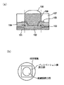
すなわち、本発明の半導体装置は、主表面を有する半導体基板と、前記主表面上に形成された電極パッドと、前記電極パッドの表面の一部を露出する第1の開口部を有し、前記主表面上を覆うパッシベーション膜と、前記電極パッドの表面の一部を露出し前記第1の開口部よりも内側に配置された第2の開口部を有し、前記パッシベーション膜上を覆う絶縁膜と、外縁を有し前記電極パッドに電気的に接続された柱状の突起電極と、前記突起電極の側面及び前記絶縁膜上を覆う封止樹脂とを有する半導体装置であって、前記第2の開口部は、前記突起電極の外縁よりも内側に配置されていることを特徴としている。
図1(b)の上面図に示すように、本実施形態においては、電極パッド102と突起電極106とは完全に重なる。具体的には、絶縁膜104の開口部(第2の開口部)の直径は突起電極106の直径より小さく、パッシベーション膜103の開口部(第1の開口部)の中心、絶縁膜104の開口部の中心、及び突起電極106の中心は略一致し、上から見たときにパッシベーション膜103及び絶縁膜104の開口部は突起電極106の中に完全に含まれる。即ち、図1(a)において、平行な点線の内側に位置するようにそれらの開口部を形成する。
Claims (4)
- 主表面を有する半導体基板と、
前記主表面上に形成された電極パッドと、
前記電極パッドの表面の一部を露出する第1の開口部を有し、前記主表面上を覆うパッシベーション膜と、
前記電極パッドの表面の一部を露出し前記第1の開口部よりも内側に配置された第2の開口部を有し、前記パッシベーション膜上を覆う絶縁膜と、
外縁を有し前記電極パッドに電気的に接続された柱状の突起電極と、
前記突起電極の側面及び前記絶縁膜上を覆う封止樹脂とを有する半導体装置であって、
前記第2の開口部は、前記突起電極の外縁よりも内側に配置されていることを特徴とする半導体装置。 - 前記第1の開口部は、前記突起電極の外縁よりも内側に配置されていることを特徴とする請求項1記載の半導体装置。
- 前記第1の開口部は、前記突起電極の外縁の直下を跨ぐように配置されていることを特徴とする請求項1記載の半導体装置。
- 主表面を有する半導体基板と、
前記主表面上に形成された複数の電極パッドであって、前記半導体基板のコーナー部に配置された第1の電極パッドと、前記コーナー部を除く領域に配置された第2の電極パッドとを含む複数の電極パッドと、
前記第1及び第2の電極パッドの各々の表面の一部を露出する第1の開口部を有し、前記主表面上を覆うパッシベーション膜と、
前記第1及び第2の電極パッドの各々の表面の一部を露出し前記第1の開口部よりも内側に配置された第2の開口部を有し、前記パッシベーション膜上を覆う絶縁膜と、
外縁を有し対応する前記電極パッドの各々に電気的に接続された複数の柱状の突起電極と、
前記突起電極の側面及び前記絶縁膜上を覆う封止樹脂とを有する半導体装置であって、
前記第2の開口部は、前記突起電極の外縁よりも内側に配置されており、前記第2の電極パッドに対応する前記第1の開口部は、前記突起電極の外縁よりも内側に配置されており、前記第1の電極パッドに対応する前記第1の開口部は、前記突起電極の外縁の直下を跨ぐように配置されていることを特徴とする半導体装置。
Priority Applications (2)
| Application Number | Priority Date | Filing Date | Title |
|---|---|---|---|
| US10/866,195 US7180185B2 (en) | 2003-06-13 | 2004-06-14 | Semiconductor device with connections for bump electrodes |
| JP2004175098A JP4165460B2 (ja) | 2003-06-13 | 2004-06-14 | 半導体装置 |
Applications Claiming Priority (2)
| Application Number | Priority Date | Filing Date | Title |
|---|---|---|---|
| JP2003169010 | 2003-06-13 | ||
| JP2004175098A JP4165460B2 (ja) | 2003-06-13 | 2004-06-14 | 半導体装置 |
Publications (2)
| Publication Number | Publication Date |
|---|---|
| JP2005026679A JP2005026679A (ja) | 2005-01-27 |
| JP4165460B2 true JP4165460B2 (ja) | 2008-10-15 |
Family
ID=34082287
Family Applications (1)
| Application Number | Title | Priority Date | Filing Date |
|---|---|---|---|
| JP2004175098A Expired - Lifetime JP4165460B2 (ja) | 2003-06-13 | 2004-06-14 | 半導体装置 |
Country Status (2)
| Country | Link |
|---|---|
| US (1) | US7180185B2 (ja) |
| JP (1) | JP4165460B2 (ja) |
Families Citing this family (11)
| Publication number | Priority date | Publication date | Assignee | Title |
|---|---|---|---|---|
| JP4381191B2 (ja) * | 2004-03-19 | 2009-12-09 | Okiセミコンダクタ株式会社 | 半導体パッケージ及び半導体装置の製造方法 |
| US7451436B2 (en) * | 2004-11-23 | 2008-11-11 | National Instruments Corporation | Aggregate handling of operator overloading |
| CN100416875C (zh) * | 2005-03-30 | 2008-09-03 | 南茂科技股份有限公司 | 使用凸块进行封装的结构及其形成方法 |
| JP5165190B2 (ja) * | 2005-06-15 | 2013-03-21 | オンセミコンダクター・トレーディング・リミテッド | 半導体装置及びその製造方法 |
| JP4430062B2 (ja) * | 2006-12-06 | 2010-03-10 | シャープ株式会社 | Icチップ実装パッケージの製造方法 |
| JP4708399B2 (ja) * | 2007-06-21 | 2011-06-22 | 新光電気工業株式会社 | 電子装置の製造方法及び電子装置 |
| US20110186899A1 (en) * | 2010-02-03 | 2011-08-04 | Polymer Vision Limited | Semiconductor device with a variable integrated circuit chip bump pitch |
| JP2012028708A (ja) | 2010-07-27 | 2012-02-09 | Renesas Electronics Corp | 半導体装置 |
| JP2012064698A (ja) * | 2010-09-15 | 2012-03-29 | Ricoh Co Ltd | 半導体装置及びそのレイアウト方法 |
| US11063009B2 (en) * | 2017-04-10 | 2021-07-13 | Renesas Electronics Corporation | Semiconductor device |
| JP7532235B2 (ja) * | 2020-12-10 | 2024-08-13 | キヤノン株式会社 | 液体吐出ヘッド及びその製造方法 |
Family Cites Families (5)
| Publication number | Priority date | Publication date | Assignee | Title |
|---|---|---|---|---|
| US5152598A (en) * | 1990-10-24 | 1992-10-06 | Schaffer Garry D | Hole locator device |
| US6739744B2 (en) * | 1997-07-02 | 2004-05-25 | Lumitex, Inc. | Light delivery systems and applications thereof |
| US5921673A (en) * | 1997-11-13 | 1999-07-13 | Habel; David M. | Illuminated threading tool |
| US6075290A (en) * | 1998-02-26 | 2000-06-13 | National Semiconductor Corporation | Surface mount die: wafer level chip-scale package and process for making the same |
| JP4394266B2 (ja) | 2000-09-18 | 2010-01-06 | カシオ計算機株式会社 | 半導体装置および半導体装置の製造方法 |
-
2004
- 2004-06-14 US US10/866,195 patent/US7180185B2/en not_active Expired - Lifetime
- 2004-06-14 JP JP2004175098A patent/JP4165460B2/ja not_active Expired - Lifetime
Also Published As
| Publication number | Publication date |
|---|---|
| US7180185B2 (en) | 2007-02-20 |
| JP2005026679A (ja) | 2005-01-27 |
| US20050017356A1 (en) | 2005-01-27 |
Similar Documents
| Publication | Publication Date | Title |
|---|---|---|
| JP4071914B2 (ja) | 半導体素子及びこれを用いた半導体装置 | |
| JP4449824B2 (ja) | 半導体装置およびその実装構造 | |
| JP5075611B2 (ja) | 半導体装置 | |
| JP3918842B2 (ja) | 半導体素子及びそれを備えたワイヤボンディング・チップサイズ・パッケージ | |
| EP2863419B1 (en) | Semiconductor device | |
| JP4165460B2 (ja) | 半導体装置 | |
| JP2015072942A (ja) | 半導体装置 | |
| JP4045261B2 (ja) | 半導体装置 | |
| JP2005236277A (ja) | 半導体集積回路 | |
| JP2009111279A (ja) | 半導体装置の配線基板、半導体装置、電子装置、マザーボード、半導体装置の配線基板の製造方法、マザーボードの製造方法、電子装置の製造方法 | |
| JP4251164B2 (ja) | 半導体装置および半導体チップ | |
| JP2009111333A (ja) | 半導体装置 | |
| JP2007059867A (ja) | 半導体装置 | |
| JP2006502561A (ja) | パッド下の集積半導体構造 | |
| JP2008078354A (ja) | 半導体装置 | |
| JP4435074B2 (ja) | 半導体装置およびその製造方法 | |
| JP4658914B2 (ja) | 半導体装置およびその製造方法 | |
| JP2007149809A (ja) | 半導体装置およびその製造方法 | |
| JP4835230B2 (ja) | 半導体装置の実装構造 | |
| JP4002161B2 (ja) | 半導体装置 | |
| JP4058630B2 (ja) | 半導体装置及びその製造方法、回路基板並びに電子機器 | |
| JP4784229B2 (ja) | 半導体装置 | |
| JP4038691B2 (ja) | 半導体装置及びその製造方法、回路基板並びに電子機器 | |
| JP4038692B2 (ja) | 半導体装置及びその製造方法、回路基板並びに電子機器 | |
| JP2005093931A (ja) | 半導体装置 |
Legal Events
| Date | Code | Title | Description |
|---|---|---|---|
| A621 | Written request for application examination |
Free format text: JAPANESE INTERMEDIATE CODE: A621 Effective date: 20060825 |
|
| RD01 | Notification of change of attorney |
Free format text: JAPANESE INTERMEDIATE CODE: A7421 Effective date: 20060923 |
|
| RD02 | Notification of acceptance of power of attorney |
Free format text: JAPANESE INTERMEDIATE CODE: A7422 Effective date: 20060929 |
|
| RD04 | Notification of resignation of power of attorney |
Free format text: JAPANESE INTERMEDIATE CODE: A7424 Effective date: 20061013 |
|
| A977 | Report on retrieval |
Free format text: JAPANESE INTERMEDIATE CODE: A971007 Effective date: 20070315 |
|
| A131 | Notification of reasons for refusal |
Free format text: JAPANESE INTERMEDIATE CODE: A131 Effective date: 20080129 |
|
| A521 | Request for written amendment filed |
Free format text: JAPANESE INTERMEDIATE CODE: A523 Effective date: 20080326 |
|
| A131 | Notification of reasons for refusal |
Free format text: JAPANESE INTERMEDIATE CODE: A131 Effective date: 20080422 |
|
| A521 | Request for written amendment filed |
Free format text: JAPANESE INTERMEDIATE CODE: A523 Effective date: 20080617 |
|
| TRDD | Decision of grant or rejection written | ||
| A01 | Written decision to grant a patent or to grant a registration (utility model) |
Free format text: JAPANESE INTERMEDIATE CODE: A01 Effective date: 20080708 |
|
| A01 | Written decision to grant a patent or to grant a registration (utility model) |
Free format text: JAPANESE INTERMEDIATE CODE: A01 |
|
| A61 | First payment of annual fees (during grant procedure) |
Free format text: JAPANESE INTERMEDIATE CODE: A61 Effective date: 20080721 |
|
| R150 | Certificate of patent or registration of utility model |
Ref document number: 4165460 Country of ref document: JP Free format text: JAPANESE INTERMEDIATE CODE: R150 Free format text: JAPANESE INTERMEDIATE CODE: R150 |
|
| FPAY | Renewal fee payment (event date is renewal date of database) |
Free format text: PAYMENT UNTIL: 20110808 Year of fee payment: 3 |
|
| FPAY | Renewal fee payment (event date is renewal date of database) |
Free format text: PAYMENT UNTIL: 20110808 Year of fee payment: 3 |
|
| S111 | Request for change of ownership or part of ownership |
Free format text: JAPANESE INTERMEDIATE CODE: R313111 |
|
| S531 | Written request for registration of change of domicile |
Free format text: JAPANESE INTERMEDIATE CODE: R313531 |
|
| FPAY | Renewal fee payment (event date is renewal date of database) |
Free format text: PAYMENT UNTIL: 20110808 Year of fee payment: 3 |
|
| R350 | Written notification of registration of transfer |
Free format text: JAPANESE INTERMEDIATE CODE: R350 |
|
| FPAY | Renewal fee payment (event date is renewal date of database) |
Free format text: PAYMENT UNTIL: 20120808 Year of fee payment: 4 |
|
| S533 | Written request for registration of change of name |
Free format text: JAPANESE INTERMEDIATE CODE: R313533 |
|
| FPAY | Renewal fee payment (event date is renewal date of database) |
Free format text: PAYMENT UNTIL: 20120808 Year of fee payment: 4 |
|
| R350 | Written notification of registration of transfer |
Free format text: JAPANESE INTERMEDIATE CODE: R350 |
|
| FPAY | Renewal fee payment (event date is renewal date of database) |
Free format text: PAYMENT UNTIL: 20120808 Year of fee payment: 4 |
|
| FPAY | Renewal fee payment (event date is renewal date of database) |
Free format text: PAYMENT UNTIL: 20130808 Year of fee payment: 5 |
|
| S531 | Written request for registration of change of domicile |
Free format text: JAPANESE INTERMEDIATE CODE: R313531 |
|
| R350 | Written notification of registration of transfer |
Free format text: JAPANESE INTERMEDIATE CODE: R350 |
|
| EXPY | Cancellation because of completion of term |