JP4181908B2 - Clock transfer circuit - Google Patents
Clock transfer circuit Download PDFInfo
- Publication number
- JP4181908B2 JP4181908B2 JP2003090699A JP2003090699A JP4181908B2 JP 4181908 B2 JP4181908 B2 JP 4181908B2 JP 2003090699 A JP2003090699 A JP 2003090699A JP 2003090699 A JP2003090699 A JP 2003090699A JP 4181908 B2 JP4181908 B2 JP 4181908B2
- Authority
- JP
- Japan
- Prior art keywords
- clock
- signal
- circuit
- phcen
- phcud
- Prior art date
- Legal status (The legal status is an assumption and is not a legal conclusion. Google has not performed a legal analysis and makes no representation as to the accuracy of the status listed.)
- Expired - Fee Related
Links
Images


Landscapes
- Stabilization Of Oscillater, Synchronisation, Frequency Synthesizers (AREA)
- Synchronisation In Digital Transmission Systems (AREA)
Description
【0001】
【発明の属する技術分野】
本発明は、入力クロックを基準として、PLL回路を用いて処理用クロックを生成し、入力データを入力クロックから処理用クロックに乗せ換える処理を行うクロック乗換回路に関し、詳しくは、入力クロックと処理用クロックの位相関係を自動的に最適に保つ機能を持たせたクロック乗換回路に関するものである。
【0002】
【従来の技術】
映像信号処理において、入力される映像信号のフォーマットや伝送方式によって、入力されたクロック周波数の1倍、2倍、4倍等のクロック周波数で信号処理を行うことがある。このようなとき、入力クロック(以下、クロックA)を基準としてPLL(Phase Locked Loop)回路を用いて処理用クロック(以下、クロックB)を生成し、入力データをクロックAからクロックBに乗せ換える処理が必要となる。
【0003】
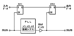
PLLを用いたクロック乗換回路の基本的な構成として、図6に示すようなものがある。この図6に示すようなクロック乗換回路では、D型−フリップフロップ(以下、DFF)のセットアップタイム、ホールドタイムを満足するように、クロックAとクロックBの位相関係を適正に設定する必要がある。しかし、PLLはクロックAとクロックBの位相を一定に保つように動作するとはいえ、クロック周波数によって異なる定常的な位相差が発生してしまう。また、クロックBは信号処理に用いるため、ファンアウトの大きなバッファを使用するが、これにより信号の遅延が大きくなってしまう。位相差、遅延がクロック周期に対して無視できない量になった場合には、周波数毎にクロックの位相関係を調整する必要があるが、高い周波数では温度変化やデバイスのばらつきにより位相関係を適正に設定できなくなる。
【0004】
そこで従来より、位相関係を調整する方法として、RAMを用いたクロック乗換回路があり、このRAMを使用した回路によれば、RAMへクロック信号を書込むタイミングとRAMからクロック信号を読出すタイミングとを制御することによって、位相関係を適正に設定することができる。
しかし、このRAMを用いた構成では回路規模が大きくなり、コストも高くなってしまうという問題があったため、RAMを必要とせず、回路規模を小さくしてコストダウンを図ることのできるクロック乗換回路が提案されている(例えば、特許文献1参照)。
【0005】
【特許文献1】
特開2002−204448号公報
【0006】
【発明が解決しようとする課題】
上記特許文献1に記載のクロック乗換回路は、RAMを必要とせず、回路規模を小さくしてコストダウンを図ることが可能であるが、この方式は、クロックBがクロックAの2倍の周波数の場合のみ対応した回路であるため、例えば、クロックBがクロックAの1倍、4倍等の周波数を持つような周波数条件には対応できないという問題があった。
【0007】
本発明は、上記問題点に鑑みなされたもので、RAM等のメモリを使用せずに、クロックBがクロックAの1倍、2倍、4倍等のどのような周波数条件であっても、クロックAとクロックBの位相関係を自動的に最適化することのできるクロック乗換回路を提供することを目的とするものである。
【0008】
【課題を解決するための手段】
本発明は、入力クロック(以下、クロックA)に対して整数倍の周波数を持った処理用クロック(以下、クロックB)を生成し、このクロックAとクロックBの位相を揃える機能を持ったPLL回路と、入力データを前記クロックAの立上りでラッチするD型フリップフロップ(以下、FF)1と、FF1の出力を前記クロックBの立下りでラッチするFF2とを具備してなるクロック乗換回路において、入力されたクロックAとクロックBの立上りを比較してクロックAの立上りに対してクロックBの立上りが早い場合はハイレベルとなり遅い場合はローレベルとなるPHCUD信号と、このPHCUD信号のイネーブル信号としてのPHCEN信号とを生成して出力する位相比較回路と、前記PHCEN信号がハイレベルのときにPHCUD信号のアップダウンをカウントして、そのカウント値がプラス又はマイナスの一定値に達したときにPHASE信号を+1又は−1してPLL回路に出力する安定化フィルタ回路とを設け、前記PLL回路では、入力されたPHASE信号に基づいてクロックAとクロックBの位相差が小さくなるように位相調整を行うようにしたことを特徴とするクロック乗換回路である。
【0009】
このような構成とすることで、RAM等のメモリを使用することなく、クロックBがクロックAの1倍、2倍、4倍等のどのような周波数条件であっても、PHCUD信号とPHCEN信号とから生成されるPHASE信号を用いて、PLL回路においてクロックAとクロックBの位相関係を自動的に最適化することができる。
【0010】
【発明の実施の形態】
本発明の実施の形態を図面に基づいて説明する。
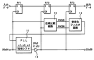
図1に示すのは、本発明によるクロック乗換回路10の構成を示したブロック図であり、このクロック乗換回路10は、FF1、FF2、FF3、PLL回路11、クロックバッファ12、位相比較回路13、安定化フィルタ回路14によって構成されている。
FF1、FF2、FF3は、D型−フリップフロップであり、D入力に入力されたデータをCK入力に入力されたクロック信号の立上りで取り込んで(ラッチして)、Q出力から出力するものである。以下、FF又はDFFという場合は、D型−フリップフロップを指すものとする。
【0011】
PLL回路11は、入力クロック(以下、クロックA)を基準として、クロック乗換処理に用いる処理用クロック(以下、クロックB)を生成するための回路であり、例えば、クロックAの1倍、2倍、4倍等の周波数を持つクロックBを生成することができる。また、クロックAとクロックBの位相関係を適正に保つように働くものでもある。
【0012】
前記FF1、FF2、FF3、PLL回路11、及び、クロックバッファ12で構成される部分については、図6に示す従来回路と略同様の構成であり、FF1のD入力に入力された入力データをクロックAの立上りでラッチして、このFF1の出力はFF2のD入力に入力されてクロックBの立下りでラッチされて出力される。なお、FF3は出力先との関係で設置されるもので、直接本発明に関わるものではない。ここで、クロックAとクロックBは、PLL回路11で位相関係が一定、具体的には、立上りのタイミングが揃うように調整されているため、クロックAでラッチしたものをクロックBで再度ラッチすることにより、クロックの乗せ換えが行われる。しかし、従来技術の記載で問題点として挙げたものと同様に、クロック周波数によって異なる定常的な位相差、及び、PLL回路11のクロックBの出力側に設けたファンアウトの大きなクロックバッファ12による信号の遅延という位相関係がずれる要因が存在するため、このままでは位相関係を適正に保つことができない。
【0013】
そこで、本発明では、クロックAとクロックBの位相関係を比較する位相比較回路13と、位相比較回路13での比較結果から位相の調整を行うためにPLL回路11の位相設定端子に対してPHASE信号を出力する安定化フィルタ回路14とを設けて、クロックAとクロックBの立上りが揃うように位相関係を調整する構成となっている。
【0014】
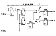
前記位相比較回路13は、クロックAの立上りに対してクロックBの立上りが早いときは“0”、遅いときは“1”となる比較結果としてのPHCUD信号と、このPHCUD信号のイネーブル信号としてのPHCEN信号を後段の安定化フィルタ回路14に出力するための回路であり、その構成を図2に示す。
図2において、FF4は、クロックAを2分周してデューティー比が略1:1のCKA2信号を生成して出力する。FF5は、FF4からのCKA2信号をクロックBの立上りでラッチして出力する。FF6は、FF4からのCKA2信号をクロックBの反転信号の立上り、つまり、クロックBの立下りでラッチして出力する。FF7は、FF6の出力をクロックBの立上りでラッチして出力する。第1XOR回路15は、FF5の出力とFF6の出力のXOR(排他的論理和)をとって出力する。第2XOR回路16は、FF6の出力とFF7の出力のXORをとって出力する。FF8は、第1XOR回路15の出力をクロックBの立上りでラッチして、これをPHCUD信号として後段の安定化フィルタ回路14に出力する。FF9は、第2XOR回路16の出力をクロックBの立上りでラッチして、これをPHCEN信号として後段の安定化フィルタ回路14に出力する。
【0015】
図5は、安定化フィルタ回路14の構成を示したブロック図である。この図5において、安定化フィルタ回路14は、第1アップ/ダウンカウンタ22と、デコーダ23と、第2アップ/ダウンカウンタ24と、PHCEN周期検出部25とからなるもので、この安定化フィルタ回路14において、PLL回路11でクロックAとクロックBの位相差を調整するためのPHASE信号を生成して出力する。
【0016】
PHCEN周期検出部25は、delay回路17、第3XOR回路18、カウンタ19、第1OR回路20、及び、第2OR回路21とから構成され、これは、クロックA立上りとクロックB立下りが略揃っているときに、PHCUD信号とPHCEN信号を強制的に“1”にして、PHASE信号を+1するためのものであり、詳しい説明については後述する。
【0017】
前記第1アップ/ダウンカウンタ22は、UD端子に位相比較回路13からのPHCUD信号が第1OR回路20を介して入力され、EN端子に位相比較回路13からのPHCEN信号が第2OR回路21を介して入力されて、PHCEN信号がハイレベルのときにPHCUD信号を取込み、その取込んだPHCUD信号が“0”のときダウンカウントし“1”のときアップカウントする。この第1アップ/ダウンカウンタ22でのカウント値は、後段のデコーダ23に出力される。ここでのカウントは、デコーダ23からの信号がLD端子に入力されるとリセットされる。
【0018】
前記デコーダ23では、入力されたカウント値をフィルタ係数で設定された値と比較して、カウント値が設定値に達している場合に、後段の第2アップ/ダウンカウンタ24をイネーブルにする信号をEN端子に出力するとともに、第2アップ/ダウンカウンタ24を1カウント分だけアップカウント又はダウンカウントさせる。ここで、フィルタ係数の設定値は正側と負側でそれぞれ設けられており、正側の設定値にカウント値が達した場合には1カウント分だけアップカウントするために“1”を第2アップ/ダウンカウンタ24のUD端子に出力し、負側の設定値にカウント値が達した場合には1カウント分だけダウンカウントするために“0”を第2アップ/ダウンカウンタ24のUD端子に出力する構成となっている。また、第2アップ/ダウンカウンタ24をイネーブルにする信号は、第1アップ/ダウンカウンタ22のLD端子とカウンタ19のLD端子にも入力されて、それぞれのカウントをリセットする信号として用いられる。
【0019】
前記第2アップ/ダウンカウンタ24では、UD端子に入力された“1”又は“0”の信号に基づいてアップカウント又はダウンカウントを行い、このカウントに対応した+1又は−1のPHASE信号が前記PLL回路11の位相設定端子に入力される。このPHASE信号がPLL回路11の位相設定端子に入力されることによって、PLL回路11は、クロックAとクロックBの位相差を打ち消す方向にクロックBの位相を変化させる。
【0020】
次に、前記位相比較回路13においてPHCUD信号とPHCEN信号を生成するまでの各波形の変化について、図2及び図3を用いて説明する。図3は、クロックAに対するクロックBの逓倍比が1倍の場合における位相比較回路13の各部の出力波形を示したもので、クロックAとクロックBの位相関係を4つのパターンに分けて説明している。以下、それぞれのパターンごとに説明する。
【0021】
[クロックA:クロックB=1:1の場合]
(a)クロックA立上りとクロックB立上りが略揃っているとき
FF4においてクロックAを2分周して生成されたCKA2信号は、それぞれFF5とFF6に入力されて、FF5ではクロックBの立上りでラッチされ、FF6ではクロックBの立下りでラッチされる。ここで、図3(a)に示すように、クロックAの立上り、つまり、CKA2の立上りとクロックBの立上りは略揃っているが、正確にはCKA2の立上りに対してクロックBの立上りが早かったり遅かったりしている状態である。このため、CKA2は規則的にハイレベルとローレベルを繰り返している波形であるのに対して、FF5の波形DFF5はハイレベルとローレベルが不規則に現れている。FF6の波形DFF6は、クロックBの立下りでラッチするのでFF5と半周期ずれてラッチされた結果、規則的にハイレベルとローレベルを繰り返す波形となっている。このFF5とFF6の出力のXORをとったものをFF8においてクロックBでラッチすると、PHCUD信号が生成される。このPHCUD信号は、クロックAの立上りよりもクロックBの立上りの方が早かった場所ではハイレベルとなり遅かった場所ではローレベルとなる信号で、その結果をクロックBに対して1周期遅れて反映させている。また、FF7ではFF6の出力をクロックBでラッチして、このFF7とFF6のXORをとって出力したものをクロックBでラッチすると、PHCEN信号が生成される。PHCEN信号は、後段の安定化フィルタ回路14においてPHCUD信号を読み込むためのイネーブル信号であり、このようなクロックA立上りとクロックB立上りが略揃っている場合には、クロックBの2周期目以降がハイレベルとなり、この間のPHCUD信号のアップダウンをカウントすると、アップが6でダウンが5となり、図示されている期間を経過した時点で、安定化フィルタ回路14の第1アップ/ダウンカウンタ22は+1だけアップカウントされることになる。
【0022】
(b)クロックBが遅いとき
図3(b)に示すように、クロックAの立上り、つまり、CKA2の立上りに対してクロックBの立上りが常に遅い場合には、DFF5とDFF6の波形は規則的に変化する波形となり、これらの信号を第1XOR回路15でXORをとったものはクロックBと同一波形の信号となる。この第1XOR回路15の出力をFF8においてクロックBでラッチすると、PHCUD信号が生成されるが、クロックAの立上りよりもクロックBの立上りの方が常に遅いため、このPHCUD信号は常にローレベルとなっている。また、クロックAの立上りに対してクロックBの立上りが常に遅い場合には、PHCEN信号はクロックBの2周期目以降がハイレベルとなり、この間のPHCUD信号のアップダウンをカウントすると、アップが0でダウンが6となり、図示されている期間を経過した時点で、安定化フィルタ回路14の第1アップ/ダウンカウンタ22は−6だけダウンカウントされることになる。ここで、デコーダ23のフィルタ係数の設定値が例えば−6になっていたとすると、カウント値が−6に達した時点で後段の第2アップ/ダウンカウンタ24にイネーブル信号を出力するとともに、第2アップ/ダウンカウンタ24を1カウント分だけダウンカウントさせる。このカウントの結果がPHASE信号としてPLL回路11の位相設定端子に入力されることによって、PLL回路11は、クロックAとクロックBの位相差を打ち消す方向にクロックBの位相を変化させる。
【0023】
(c)クロックA立上りとクロックB立下りが略揃っているとき
図3(c)に示すように、クロックAの立上り、つまり、CKA2の立上りとクロックBの立下りが略揃っている場合には、FF5の波形DFF5は、規則的にハイレベルとローレベルを繰り返す波形となっているのに対して、FF6の波形DFF6は、ハイレベルとローレベルが不規則に現れている。これらの信号を第1XOR回路15でXORをとったものをFF8においてクロックBでラッチすると、PHCUD信号が生成される。このPHCUD信号は、クロックAの立上りよりもクロックBの立下りの方が早かった場所ではローレベルとなり遅かった場所ではハイレベルとなる信号である。これは図3の(a)や(b)の場合とハイレベルとローレベルの対応関係が逆であるが、立下りが遅い=立上りが早い、という関係にあると言えるので問題はない。また、クロックAの立上りとクロックBの立下りが略揃っている場合には、図3(c)に示すように、PHCEN信号はハイレベルとローレベルが不規則に現れる波形となっている。このときのPHCUD信号のアップダウンをカウントすると、アップが3でダウンが4となり、図示されている期間を経過した時点で、安定化フィルタ回路14の第1アップ/ダウンカウンタ22は−1だけダウンカウントされることになる。
【0024】
上記図3(c)に示すような、クロックAの立上りとクロックBの立下りが略揃っている場合には、クロックAとクロックBの立ち上がり同士が揃うように、早期に位相調整を行いたいが、PHCUD信号及びPHCEN信号が共に、ハイレベルとローレベルが不規則に現れる波形であるため、第1アップ/ダウンカウンタ22のカウントがなかなか設定値に達せず、PLL回路11に入力するPHASE信号が適正値に達するのに時間がかかり過ぎるという問題があった。
【0025】
この問題を解消するため、PHCEN周期検出部25でPHCEN信号の周期の乱れを検出する。図5に示す安定化フィルタ回路14のPHCEN周期検出部25において、第3XOR回路18は、PHCEN信号とこのPHCEN信号にdelay回路17を介して一定周期分遅延させた信号とのXORをとって出力するためのもので、この出力はカウンタ19のEN端子に入力される。この第3XOR回路18では、遅延させた信号とのXORを演算することによって、遅延前と遅延後のPHCEN信号の変化を検出することができ、変化している場合のみ“1”を出力する。ここで、delay回路17における遅延量は、PLL回路11での逓倍比によって異なり、1倍のときは遅延量1、2倍のときは遅延量2、4倍のときは遅延量4となるようにする。カウンタ19では、この第3XOR回路18で検出したPHCEN信号の変化をカウントし、このカウント値が一定回数以上になった場合に、第1アップ/ダウンカウンタ22に入力されるPHCUD信号とPHCEN信号を強制的に“1”にするために、第1OR回路20と第2OR回路21にそれぞれ“1”を出力することによってPHCUD信号とPHCEN信号の内容に関わらず、第1アップ/ダウンカウンタ22のUD端子とEN端子には必ず“1”が入力されることになる。このような構成とすることによって、PHCUD信号及びPHCEN信号が共に、ハイレベルとローレベルが不規則に現れる状態であっても、PHASE信号を+1してクロックAの立上りとクロックBの立下りが略揃っている状態から早期に抜け出すことができる。
【0026】
(d)クロックBが早いとき
図3(d)に示すように、クロックAの立上り、つまり、CKA2の立上りに対してクロックBの立上りが常に早い場合には、DFF5とDFF6の波形は規則的に変化する波形となり、これらの信号を第1XOR回路15でXORをとったものはクロックBの反転信号と同一の波形となる。この第1XOR回路15の出力をFF8においてクロックBでラッチすると、PHCUD信号が生成されるが、クロックAの立上りよりもクロックBの立上りの方が常に早いため、このPHCUD信号は2周期目以降が常にハイレベルとなっている。また、PHCEN信号も同様に、クロックBの2周期目以降がハイレベルとなり、この間のPHCUD信号のアップダウンをカウントすると、アップが6でダウンが0となり、図示されている期間を経過した時点で、安定化フィルタ回路14の第1アップ/ダウンカウンタ22は+6だけアップカウントされることになる。ここで、デコーダ23のフィルタ係数の設定値が例えば+6になっていたとすると、カウント値が+6に達した時点で後段の第2アップ/ダウンカウンタ24にイネーブル信号を出力するとともに、第2アップ/ダウンカウンタ24を1カウント分だけアップカウントさせる。このカウントの結果がPHASE信号としてPLL回路11の位相設定端子に入力されることによって、PLL回路11は、クロックAとクロックBの位相差を打ち消す方向にクロックBの位相を変化させる。
【0027】
このように、本発明のクロック乗換回路は、位相比較回路13において、クロックAの立上りに対してクロックBの立上りの方が早い場合はハイレベルとなり遅い場合はローレベルというように位相のずれが反映されたPHCUD信号と、PHCUD信号をイネーブルするためのPHCEN信号を生成し、これらのPHCUD信号とPHCEN信号を用いて位相調整を行うためのPHASE信号を生成して、このPHASE信号が入力されるPLL回路11において位相を調整するようにしている。よって、常にクロックAとクロックBの位相関係がフィードバックされることにより、位相差が打ち消されるように変化して行き、最終的にクロックAの立上りをクロックBの立上りが前後するような形で位相差は小さく維持される。
【0028】
前記実施例では、クロックAとクロックBの周波数の比が1:1の場合を例として本発明のクロック乗換回路について説明してきたが、本発明はこれに限られるものではなく、周波数比が他の場合であっても対応できるものである。ここで、クロックAとクロックBの周波数の比が1:4である場合の位相比較回路13の動作について、図4を用いて説明する。
【0029】
[クロックA:クロックB=1:4の場合]
(a)クロックA立上りとクロックB立上りが略揃っているとき
図4(a)は、クロックA:クロックB=1:4の場合におけるクロックA立上りとクロックB立上りが略揃っているときの位相比較回路13での各部の波形を示したもので、前記実施例の場合と同様に、FF4においてクロックAを2分周して生成されたCKA2信号は、それぞれFF5とFF6に入力されて、FF5ではクロックBの立上りでラッチされ、FF6ではクロックBの立下りでラッチされる。クロックAの立上りとクロックBの立上りが略揃っている場合は、正確にはCKA2の立上りに対してクロックBの立上りが早かったり遅かったりしている状態である。このため、CKA2は規則的にハイレベルとローレベルを繰り返している波形であるのに対して、FF5の波形DFF5はハイレベルとローレベルが不規則に現れている。FF6の波形DFF6は、クロックBの立下りでラッチするのでFF5と半周期ずれてラッチされた結果、規則的にハイレベルとローレベルを繰り返す波形となっている。このFF5とFF6の出力のXORをとったものをFF8においてクロックBでラッチすると、PHCUD信号が生成される。また、FF7ではFF6の出力をクロックBでラッチして、このFF7とFF6のXORをとって出力したものをクロックBでラッチすると、PHCEN信号が生成される。PHCEN信号は、クロックBの4周期に1回の間隔でハイレベルになる信号で、このハイレベルのときのPHCUD信号のアップダウンをカウントすると、アップが2でダウンが1となり、図示されている期間を経過した時点で、安定化フィルタ回路14の第1アップ/ダウンカウンタ22は+1だけアップカウントされることになる。
【0030】
(b)クロックBが遅いとき
図4(b)に示すように、クロックAの立上りに対してクロックBの立上りが常に遅い場合には、DFF5とDFF6の波形は規則的に変化する波形となり、これらの信号を第1XOR回路15においてXORをとる。この第1XOR回路15の出力をFF8においてクロックBでラッチすると、PHCUD信号が生成されるが、クロックAの立上りよりもクロックBの立上りの方が常に遅いため、このPHCUD信号は常にローレベルとなっている。また、クロックAの立上りに対してクロックBの立上りが常に遅い場合には、PHCEN信号はクロックBの4周期に1回の間隔でハイレベルとなる信号であり、このときのPHCUD信号のアップダウンをカウントすると、アップが0でダウンが2となり、図示されている期間を経過した時点で、安定化フィルタ回路14の第1アップ/ダウンカウンタ22は−2だけダウンカウントされることになる。
【0031】
(c)クロックA立上りとクロックB立下りが略揃っているとき
図4(c)に示すように、クロックAの立上りとクロックBの立下りが略揃っている場合には、FF5の波形DFF5は、規則的にハイレベルとローレベルを繰り返す波形となっているのに対して、FF6の波形DFF6は、ハイレベルとローレベルが不規則に現れている。これらの信号を第1XOR回路15でXORをとったものをFF8においてクロックBでラッチすると、PHCUD信号が生成される。このPHCUD信号は、クロックAの立上りよりもクロックBの立下りの方が早かった場所ではローレベルとなり遅かった場所ではハイレベルとなる信号である。これは図4の(a)や(b)の場合とハイレベルとローレベルの対応関係が逆であるが、立下りが遅い=立上りが早い、という関係にあると言えるので問題はない。また、クロックAの立上りとクロックBの立下りが略揃っている場合には、図4(c)に示すように、PHCEN信号はハイレベルとローレベルの周期が不規則になっている。このときのPHCUD信号のアップダウンをカウントすると、アップが1でダウンが2となり、図示されている期間を経過した時点で、安定化フィルタ回路14の第1アップ/ダウンカウンタ22は−1だけダウンカウントされることになる。
【0032】
この図4(c)に示すような、クロックAの立上りとクロックBの立下りが略揃っている場合には、クロックAとクロックBの立ち上がり同士が揃うように早期に位相調整を行うために、図3(c)の場合と同様に、図5に示す安定化フィルタ回路14のPHCEN周期検出部25において、PHCEN信号の周期の乱れを検出する。第3XOR回路18において、PHCEN信号とこのPHCEN信号にdelay回路17を介して一定周期分遅延させた信号とのXORをとって出力し、この出力はカウンタ19のEN端子に入力される。この第3XOR回路18では、遅延させた信号とのXORを演算することによって、遅延前と遅延後のPHCEN信号の変化を検出することができ、変化している場合のみ“1”を出力する。ここで、delay回路17における遅延量は、PLL回路11での逓倍比によって異なり、図4の場合は逓倍比が4であるので遅延量は4となる。カウンタ19では、この第3XOR回路18で検出したPHCEN信号の変化をカウントし、このカウント値が一定回数以上になった場合に、第1アップ/ダウンカウンタ22に入力されるPHCUD信号とPHCEN信号を強制的に“1”にして出力するようになっている。このような構成とすることによって、PHCUD信号及びPHCEN信号が共に、ハイレベルとローレベルが不規則に現れる状態であっても、PHASE信号を+1してクロックAの立上りとクロックBの立下りが略揃っている状態から早期に抜け出すことができる。
【0033】
(d)クロックBが早いとき
図4(d)に示すように、クロックAの立上りに対してクロックBの立上りが常に早い場合には、DFF5とDFF6の波形は規則的に変化する波形となり、これらの信号を第1XOR回路15でXORをとって出力する。この第1XOR回路15の出力をFF8においてクロックBでラッチすると、クロックBの4周期に1回の間隔でハイレベルとなるPHCUD信号が生成される。また、同じタイミングでPHCEN信号もクロックBの4周期に1回の間隔でハイレベルとなり、この間のPHCUD信号のアップダウンをカウントすると、アップが2でダウンが0となり、図示されている期間を経過した時点で、安定化フィルタ回路14の第1アップ/ダウンカウンタ22は+2だけアップカウントされることになる。
【0034】
上記実施例ではPLL回路11の逓倍比が1の場合と4の場合を用いて説明を行ったが、クロックAとクロックBの周波数の比が整数倍であれば、本発明のクロック乗換回路における位相比較回路13を用いることによって2つの信号の位相関係が反映されたPHCUD信号とPHCEN信号を生成することができる。このように、PHCUD信号とPHCEN信号にクロックAに対するクロックBの位相が早い又は遅いという情報が正確に反映されるため、安定化フィルタ回路14ではこのPHCUD信号とPHCEN信号からPHASE信号を生成してPLL回路11に出力するだけで、PLL回路11でクロックAとクロックBの位相差を小さく維持することができる。
【0035】
【発明の効果】
請求項1記載の発明によれば、入力クロック(以下、クロックA)に対して整数倍の周波数を持った処理用クロック(以下、クロックB)を生成し、このクロックAとクロックBの位相を揃える機能を持ったPLL回路と、入力データを前記クロックAの立上りでラッチするD型フリップフロップ(以下、FF)1と、FF1の出力を前記クロックBの立下りでラッチするFF2とを具備してなるクロック乗換回路において、入力されたクロックAとクロックBの立上りを比較してクロックAの立上りに対してクロックBの立上りが早い場合はハイレベルとなり遅い場合はローレベルとなるPHCUD信号と、このPHCUD信号のイネーブル信号としてのPHCEN信号とを生成して出力する位相比較回路と、前記PHCEN信号がハイレベルのときにPHCUD信号のアップダウンをカウントして、そのカウント値がプラス又はマイナスの一定値に達したときにPHASE信号を+1又は−1してPLL回路に出力する安定化フィルタ回路とを設け、前記PLL回路では、入力されたPHASE信号に基づいてクロックAとクロックBの位相差が小さくなるように位相調整を行うようにしたので、RAM等のメモリを使用することなく、クロックBがクロックAの1倍、2倍、4倍等のどのような周波数条件であっても、PHCUD信号とPHCEN信号とから生成されるPHASE信号を用いて、PLL回路においてクロックAとクロックBの位相関係を自動的に最適化することができる。
【0036】
請求項2記載の発明によれば、位相比較回路は、クロックAを2分周してCKA2信号を生成するFF4と、CKA2信号をクロックBの立上りでラッチするFF5と、CKA2信号をクロックBの立下りでラッチするFF6と、FF6の出力をクロックBの立上りでラッチするFF7と、FF5とFF6の出力の排他的論理和を演算する第1XOR回路と、FF6とFF7の出力の排他的論理和を演算する第2XOR回路と、第1XOR回路の出力をクロックBの立上りでラッチするFF8と、第2XOR回路の出力をクロックBの立上りでラッチするFF9とからなり、FF8の出力をPHCUD信号とし、FF9の出力をPHCEN信号として出力するようにしたので、クロックAの立上りに対してクロックBの立上りが早い場合はハイレベルとなり遅い場合はローレベルとなるPHCUD信号と、このPHCUD信号のイネーブル信号としてのPHCEN信号とを生成することができる。
【0037】
請求項3記載の発明によれば、安定化フィルタ回路は、PHCUD信号とPHCEN信号とが入力され、PHCEN信号がハイレベルかつPHCUD信号がハイレベルのときアップカウントし、PHCEN信号がハイレベルかつPHCUD信号がローレベルのときダウンカウントする第1アップ/ダウンカウンタと、第1アップ/ダウンカウンタのカウント値が予め設定されているフィルタ係数の値に達した場合に後段の第2アップ/ダウンカウンタに第1アップ/ダウンカウンタでのカウントの符号とイネーブル信号を出力するデコーダと、デコーダからのカウントの符号とイネーブル信号が入力されると、その符号が正の場合はアップカウント、負の場合はダウンカウントし、そのカウント値をPHASE信号としてPLL回路に出力する第2アップ/ダウンカウンタと、PHCEN信号の周期の乱れを検出したときにPHCUD信号とPHCEN信号を強制的にハイレベルにするPHCEN周期検出部とからなるようにしたので、PLL回路において位相を最適化する際に用いるPHASE信号をPHCUD信号とPHCEN信号とから生成することができる。
【0038】
請求項4記載の発明によれば、PHCEN周期検出部は、PHCEN信号を一定周期遅延させるdelay回路と、PHCEN信号とdelay回路との排他的論理和を演算する第3XOR回路と、第3XOR回路18からの入力がハイレベルのときにカウントし、このカウント値が一定回数以上になった場合に第1アップ/ダウンカウンタ22に入力されるPHCUD信号とPHCEN信号を強制的に“1”にして出力するカウンタとからなるようにしたので、クロックAの立上りとクロックBの立下りが略揃っている状態から早期に抜け出すことができる。
【図面の簡単な説明】
【図1】本発明によるクロック乗換回路の構成を示したブロック図である。
【図2】図1における位相比較回路の構成を示したブロック図である。
【図3】クロックAとクロックBの周波数の比が1:1である場合において、位相比較回路でPHCUD信号とPHCEN信号を生成するまでの各部の信号を示した波形図である。
【図4】クロックAとクロックBの周波数の比が1:4である場合において、位相比較回路でPHCUD信号とPHCEN信号を生成するまでの各部の信号を示した波形図である。
【図5】図1における安定化フィルタ回路の構成を示したブロック図である。
【図6】従来のクロック乗換回路の構成を示したブロック図である。
【符号の説明】
11…PLL回路、12…クロックバッファ、13…位相比較回路、14…安定化フィルタ回路、15…第1XOR回路、16…第2XOR回路、17…delay回路、18…第3XOR回路、19…カウンタ、20…第1OR回路、21…第2OR回路、22…第1アップ/ダウンカウンタ、23…デコーダ、24…第2アップ/ダウンカウンタ、25…PHCEN周期検出部。[0001]
BACKGROUND OF THE INVENTION
The present invention relates to a clock transfer circuit that generates a processing clock using a PLL circuit with reference to an input clock, and performs a process of transferring input data from the input clock to the processing clock. The present invention relates to a clock transfer circuit having a function of automatically maintaining an optimum phase relationship of clocks.
[0002]
[Prior art]
In video signal processing, signal processing may be performed at a clock frequency such as 1, 2 or 4 times the input clock frequency depending on the format or transmission method of the input video signal. In such a case, a processing clock (hereinafter referred to as clock B) is generated using a PLL (Phase Locked Loop) circuit on the basis of the input clock (hereinafter referred to as clock A), and input data is transferred from clock A to clock B. Processing is required.
[0003]
A basic configuration of a clock transfer circuit using a PLL is as shown in FIG. In the clock transfer circuit as shown in FIG. 6, it is necessary to appropriately set the phase relationship between the clock A and the clock B so as to satisfy the setup time and hold time of the D-type flip-flop (hereinafter referred to as DFF). . However, although the PLL operates so as to keep the phases of the clock A and the clock B constant, a steady phase difference that varies depending on the clock frequency occurs. In addition, since the clock B is used for signal processing, a buffer with a large fanout is used, but this increases the signal delay. If the phase difference and delay are indistinguishable with respect to the clock period, it is necessary to adjust the clock phase relationship for each frequency, but at high frequencies, the phase relationship is appropriately adjusted due to temperature changes and device variations. Cannot be set.
[0004]
Therefore, conventionally, there is a clock transfer circuit using a RAM as a method for adjusting the phase relationship. According to a circuit using this RAM, the timing for writing the clock signal to the RAM and the timing for reading the clock signal from the RAM are as follows. By controlling this, the phase relationship can be set appropriately.
However, the configuration using the RAM has a problem that the circuit scale becomes large and the cost becomes high. Therefore, a clock transfer circuit that does not require a RAM and can reduce the circuit scale and reduce the cost is provided. It has been proposed (see, for example, Patent Document 1).
[0005]
[Patent Document 1]
JP 2002-204448 A
[0006]
[Problems to be solved by the invention]
The clock transfer circuit described in Patent Document 1 does not require a RAM and can reduce the cost by reducing the circuit scale. However, in this method, the clock B has a frequency twice that of the clock A. For example, since the circuit is compatible only with the case, there is a problem that the frequency condition in which the clock B has a frequency such as 1 or 4 times that of the clock A cannot be handled.
[0007]
The present invention has been made in view of the above problems, and without using a memory such as a RAM, the clock B can be any frequency condition such as 1 time, 2 times, 4 times the clock A, etc. An object of the present invention is to provide a clock transfer circuit capable of automatically optimizing the phase relationship between the clock A and the clock B.
[0008]
[Means for Solving the Problems]
The present invention generates a processing clock (hereinafter referred to as clock B) having a frequency that is an integral multiple of the input clock (hereinafter referred to as clock A), and has a function of aligning the phases of the clock A and clock B. In a clock transfer circuit comprising a circuit, a D-type flip-flop (hereinafter referred to as FF) 1 that latches input data at the rising edge of the clock A, and FF2 that latches an output of FF1 at the falling edge of the clock B The input clock A and the rising edge of the clock B are compared, the PHCUD signal which becomes high level when the rising edge of the clock B is earlier than the rising edge of the clock A and becomes low when the clock B is late, and the enable signal of the PHCUD signal A phase comparison circuit that generates and outputs a PHCEN signal, and a PHC signal when the PCHEN signal is at a high level A stabilizing filter circuit that counts up and down of the D signal, and outputs the PHASE signal to the PLL circuit by adding +1 or -1 when the count value reaches a positive or negative constant value; The clock transfer circuit is characterized in that phase adjustment is performed based on the input PHASE signal so that the phase difference between the clock A and the clock B becomes small.
[0009]
With such a configuration, the PHCUD signal and the PHCEN signal can be used regardless of the frequency condition of the clock B being 1, 2 or 4 times the clock A without using a memory such as a RAM. The phase relationship between the clock A and the clock B can be automatically optimized in the PLL circuit using the PHASE signal generated from.
[0010]
DETAILED DESCRIPTION OF THE INVENTION
Embodiments of the present invention will be described with reference to the drawings.
FIG. 1 is a block diagram showing the configuration of a clock transfer circuit 10 according to the present invention. This clock transfer circuit 10 includes FF1, FF2, FF3,
FF1, FF2, and FF3 are D-type flip-flops that take in (latched) the data input to the D input at the rising edge of the clock signal input to the CK input and output from the Q output. . Hereinafter, FF or DFF refers to a D-type flip-flop.
[0011]
The
[0012]
The portion composed of the FF1, FF2, FF3,
[0013]
Therefore, in the present invention, the
[0014]
The
In FIG. 2, the FF 4 divides the clock A by two to generate and output a CKA2 signal having a duty ratio of approximately 1: 1. The FF5 latches and outputs the CKA2 signal from the FF4 at the rising edge of the clock B. The FF 6 latches and outputs the
[0015]
FIG. 5 is a block diagram showing the configuration of the
[0016]
The PHCEN
[0017]
In the first up / down
[0018]
The
[0019]
The second up / down
[0020]
Next, changes in each waveform until the PHCUD signal and the PHCEN signal are generated in the
[0021]
[Clock A: Clock B = 1: 1]
(A) When clock A rise and clock B rise are substantially aligned
The CKA2 signal generated by dividing the clock A by 2 in the FF4 is input to the FF5 and the FF6, respectively, latched at the rising edge of the clock B in the FF5, and latched at the falling edge of the clock B in the FF6. Here, as shown in FIG. 3A, the rising edge of the clock A, that is, the rising edge of the CKA2 and the rising edge of the clock B are substantially aligned, but precisely the rising edge of the clock B is earlier than the rising edge of the CKA2. Or slow. For this reason, CKA2 is a waveform that regularly repeats a high level and a low level, whereas the waveform DFF5 of FF5 appears irregularly in the high level and the low level. Since the waveform DFF6 of FF6 is latched at the falling edge of the clock B, it is latched with a half-cycle shift from FF5. As a result, the waveform DFF6 regularly repeats a high level and a low level. When the XORed outputs of the FF5 and FF6 are latched by the clock B in the FF8, a PHCUD signal is generated. This PHCUD signal is a signal that is at a high level at a place where the rising edge of the clock B is earlier than a rising edge of the clock A, and is at a low level at a place where the clock B is late. ing. In FF7, the output of FF6 is latched with clock B, and the XORed output of FF7 and FF6 is latched with clock B to generate the PHCEN signal. The PHCEN signal is an enable signal for reading the PHCUD signal in the
[0022]
(B) When clock B is slow
As shown in FIG. 3B, when the rising edge of the clock A, that is, when the rising edge of the clock B is always slower than the rising edge of the CKA2, the waveforms of the DFF5 and the DFF6 change regularly. A signal obtained by XORing the signal by the
[0023]
(C) When clock A rising edge and clock B falling edge are substantially aligned
As shown in FIG. 3C, when the rising edge of the clock A, that is, when the rising edge of the CKA2 and the falling edge of the clock B are substantially aligned, the waveform DFF5 of the FF5 has a regular high level and low level. The waveform DFF6 of FF6 appears irregularly in the waveform DFF6 of the FF6, while the waveform repeats. When these signals obtained by XORing with the
[0024]
When the rising edge of clock A and the falling edge of clock B are substantially aligned as shown in FIG. 3C, phase adjustment is desired to be performed early so that the rising edges of clock A and clock B are aligned. However, since both the PHCUD signal and the PHCEN signal are waveforms in which the high level and the low level appear irregularly, the count of the first up / down
[0025]
In order to solve this problem, the
[0026]
(D) When clock B is early
As shown in FIG. 3D, when the rising edge of the clock A, that is, when the rising edge of the clock B is always faster than the rising edge of the CKA2, the waveforms of the DFF5 and the DFF6 change regularly. The signal obtained by XORing the signal by the
[0027]
As described above, in the clock transfer circuit of the present invention, in the
[0028]
In the above embodiment, the clock transfer circuit of the present invention has been described by taking the case where the ratio of the frequency of the clock A and the clock B is 1: 1 as an example. However, the present invention is not limited to this, and the frequency ratio is not limited to this. Even in the case of, it can cope. Here, the operation of the
[0029]
[Clock A: Clock B = 1: 4]
(A) When clock A rise and clock B rise are substantially aligned
FIG. 4A shows the waveform of each part in the
[0030]
(B) When clock B is slow
As shown in FIG. 4B, when the rising edge of the clock B is always slower than the rising edge of the clock A, the waveforms of the DFF5 and DFF6 change regularly, and these signals are converted into the
[0031]
(C) When clock A rising edge and clock B falling edge are substantially aligned
As shown in FIG. 4C, when the rising edge of the clock A and the falling edge of the clock B are substantially aligned, the waveform DFF5 of the FF5 is a waveform that regularly repeats the high level and the low level. On the other hand, in the waveform DFF6 of FF6, the high level and the low level appear irregularly. When these signals obtained by XORing with the
[0032]
When the rising edge of clock A and the falling edge of clock B are substantially aligned as shown in FIG. 4C, the phase adjustment is performed early so that the rising edges of clock A and clock B are aligned. Similarly to the case of FIG. 3C, the PUCEN
[0033]
(D) When clock B is early
As shown in FIG. 4D, when the rising edge of the clock B is always faster than the rising edge of the clock A, the waveforms of the DFF5 and DFF6 change regularly, and these signals are converted into the
[0034]
In the above embodiment, the case where the multiplication ratio of the
[0035]
【The invention's effect】
According to the first aspect of the present invention, a processing clock (hereinafter referred to as clock B) having a frequency that is an integral multiple of the input clock (hereinafter referred to as clock A) is generated, and the phases of the clock A and clock B are determined. A PLL circuit having a function of aligning, a D-type flip-flop (hereinafter referred to as FF) 1 that latches input data at the rising edge of the clock A, and an FF2 that latches the output of FF1 at the falling edge of the clock B. In the clock transfer circuit, the rising edges of the input clock A and the clock B are compared, and when the rising edge of the clock B is earlier than the rising edge of the clock A, the PHCUD signal becomes a high level, and when late, the PHCUD signal becomes a low level; A phase comparison circuit that generates and outputs a PHCEN signal as an enable signal of the PHCUD signal, and the PHCEN signal is high-level. And a stabilizing filter circuit that counts up and down of the PHCUD signal at the time of the signal and outputs the PHASE signal to the PLL circuit by incrementing the PHASE signal by +1 or -1 when the count value reaches a positive or negative constant value. In the PLL circuit, since the phase adjustment is performed so that the phase difference between the clock A and the clock B becomes small based on the input PHASE signal, the clock B can be generated without using a memory such as a RAM. The phase relationship between the clock A and the clock B is changed in the PLL circuit using the PHASE signal generated from the PHCUD signal and the PHCEN signal under any frequency condition such as 1 time, 2 times, 4 times A, etc. It can be optimized automatically.
[0036]
According to the second aspect of the present invention, the phase comparison circuit divides the clock A by 2 to generate the CKA2 signal, the FF5 that latches the CKA2 signal at the rising edge of the clock B, and the CKA2 signal to the clock B. FF6 that latches at the falling edge, FF7 that latches the output of FF6 at the rising edge of clock B, a first XOR circuit that calculates an exclusive OR of the outputs of FF5 and FF6, and an exclusive OR of the outputs of FF6 and FF7 A second XOR circuit that calculates the output of the first XOR circuit at the rising edge of the clock B, and an FF9 that latches the output of the second XOR circuit at the rising edge of the clock B. The output of the FF8 is a PHCUD signal. Since the output of the FF 9 is output as the PHCEN signal, if the rising edge of the clock B is earlier than the rising edge of the clock A, If slow level so may generate a PHCUD signal becomes low level, and PHCEN signal as the enable signal of the PHCUD signal.
[0037]
According to the third aspect of the present invention, the stabilization filter circuit is configured to count up when the PHCUD signal and the PHCEN signal are input, the PHCEN signal is high level and the PHCUD signal is high level, and the PHCEN signal is high level and PHCUD. A first up / down counter that counts down when the signal is at a low level, and a second up / down counter in the subsequent stage when the count value of the first up / down counter reaches a preset filter coefficient value A decoder that outputs the sign and enable signal of the count in the first up / down counter, and the count sign and enable signal from the decoder when the sign is positive, it counts up when the sign is positive, and down when it is negative Counts and outputs the count value to the PLL circuit as a PHASE signal Since the second up / down counter and the PHCEN signal detector forcibly setting the PHCUD signal and the PHCEN signal to a high level when a disturbance in the PHCEN signal cycle is detected, the phase is optimized in the PLL circuit. The PHASE signal used for the conversion can be generated from the PHCUD signal and the PHCEN signal.
[0038]
According to the fourth aspect of the present invention, the PHCEN cycle detection unit includes a delay circuit that delays the PHCEN signal by a predetermined cycle, a third XOR circuit that calculates an exclusive OR of the PHCEN signal and the delay circuit, and a
[Brief description of the drawings]
FIG. 1 is a block diagram showing a configuration of a clock transfer circuit according to the present invention.
2 is a block diagram showing a configuration of a phase comparison circuit in FIG. 1. FIG.
FIG. 3 is a waveform diagram showing signals at various parts until a phase comparison circuit generates a PHCUD signal and a PHCEN signal when the ratio of the frequency of clock A to clock B is 1: 1.
FIG. 4 is a waveform diagram showing signals at various parts until a phase comparison circuit generates a PHCUD signal and a PHCEN signal when the ratio of the frequencies of clock A and clock B is 1: 4.
5 is a block diagram showing a configuration of a stabilizing filter circuit in FIG. 1. FIG.
FIG. 6 is a block diagram showing a configuration of a conventional clock transfer circuit.
[Explanation of symbols]
DESCRIPTION OF
Claims (4)
Priority Applications (1)
| Application Number | Priority Date | Filing Date | Title |
|---|---|---|---|
| JP2003090699A JP4181908B2 (en) | 2003-03-28 | 2003-03-28 | Clock transfer circuit |
Applications Claiming Priority (1)
| Application Number | Priority Date | Filing Date | Title |
|---|---|---|---|
| JP2003090699A JP4181908B2 (en) | 2003-03-28 | 2003-03-28 | Clock transfer circuit |
Publications (2)
| Publication Number | Publication Date |
|---|---|
| JP2004297703A JP2004297703A (en) | 2004-10-21 |
| JP4181908B2 true JP4181908B2 (en) | 2008-11-19 |
Family
ID=33404252
Family Applications (1)
| Application Number | Title | Priority Date | Filing Date |
|---|---|---|---|
| JP2003090699A Expired - Fee Related JP4181908B2 (en) | 2003-03-28 | 2003-03-28 | Clock transfer circuit |
Country Status (1)
| Country | Link |
|---|---|
| JP (1) | JP4181908B2 (en) |
Families Citing this family (3)
| Publication number | Priority date | Publication date | Assignee | Title |
|---|---|---|---|---|
| KR100968225B1 (en) | 2008-03-28 | 2010-07-06 | 주식회사 한영넉스 | Counter Filter Using De-Flip-Flop |
| JP4995325B2 (en) * | 2008-07-25 | 2012-08-08 | 株式会社アドバンテスト | Clock transfer circuit and test apparatus using the same |
| JP7393079B2 (en) * | 2019-03-26 | 2023-12-06 | ラピスセミコンダクタ株式会社 | semiconductor equipment |
-
2003
- 2003-03-28 JP JP2003090699A patent/JP4181908B2/en not_active Expired - Fee Related
Also Published As
| Publication number | Publication date |
|---|---|
| JP2004297703A (en) | 2004-10-21 |
Similar Documents
| Publication | Publication Date | Title |
|---|---|---|
| JP4406897B2 (en) | Delay locked loop | |
| US5506878A (en) | Programmable clock having programmable delay and duty cycle based on a user-supplied reference clock | |
| EP1139569A1 (en) | Adjustment of the duty-cycle of a periodic digital signal with leading and triling edge DLLs | |
| KR101050406B1 (en) | Duty Correction Circuit and Clock Generation Circuit Including It | |
| US8242822B2 (en) | Delay locked loop | |
| CN101485091A (en) | Method and apparatus for reducing oscillation in synchronous circuits | |
| CN104283556A (en) | Clock delay detection circuit and semiconductor device using clock delay detection circuit | |
| KR20140010658A (en) | Semiconductor device | |
| JP4181908B2 (en) | Clock transfer circuit | |
| JP5448324B2 (en) | DLL circuit, semiconductor device including the same, and data processing system | |
| US7187598B1 (en) | Device having an interface and method thereof | |
| CN110534142B (en) | Synchronous circuit and method related to synchronous circuit | |
| KR20040023838A (en) | Register controlled delay locked loop | |
| US6573698B2 (en) | Clock synchronizing method and circuit varying a phase of a synchronous clock in one direction or the other according to a phase difference of the synchronous clock from a reference clock | |
| KR20140090300A (en) | Latency control circuit and semiconductor memory device including the same | |
| JP3776895B2 (en) | Phase adjustment circuit | |
| JP3934504B2 (en) | Binary circuit | |
| US7375558B2 (en) | Method and apparatus for pre-clocking | |
| KR20030049303A (en) | Register Controlled DLL Circuit | |
| JP3116600B2 (en) | Timing generator | |
| JPH05315898A (en) | Trigger synchronization circuit | |
| JPH11220369A (en) | Clock detecting circuit | |
| JP3957200B2 (en) | Delay control device | |
| JP3280724B2 (en) | Image interface circuit | |
| JP5315882B2 (en) | Semiconductor device and communication method |
Legal Events
| Date | Code | Title | Description |
|---|---|---|---|
| A621 | Written request for application examination |
Free format text: JAPANESE INTERMEDIATE CODE: A621 Effective date: 20060327 |
|
| A711 | Notification of change in applicant |
Free format text: JAPANESE INTERMEDIATE CODE: A711 Effective date: 20080515 |
|
| A977 | Report on retrieval |
Free format text: JAPANESE INTERMEDIATE CODE: A971007 Effective date: 20080605 |
|
| A521 | Written amendment |
Free format text: JAPANESE INTERMEDIATE CODE: A523 Effective date: 20080620 |
|
| TRDD | Decision of grant or rejection written | ||
| A01 | Written decision to grant a patent or to grant a registration (utility model) |
Free format text: JAPANESE INTERMEDIATE CODE: A01 Effective date: 20080826 |
|
| A01 | Written decision to grant a patent or to grant a registration (utility model) |
Free format text: JAPANESE INTERMEDIATE CODE: A01 |
|
| A61 | First payment of annual fees (during grant procedure) |
Free format text: JAPANESE INTERMEDIATE CODE: A61 Effective date: 20080901 |
|
| R150 | Certificate of patent or registration of utility model |
Free format text: JAPANESE INTERMEDIATE CODE: R150 |
|
| FPAY | Renewal fee payment (event date is renewal date of database) |
Free format text: PAYMENT UNTIL: 20110905 Year of fee payment: 3 |
|
| FPAY | Renewal fee payment (event date is renewal date of database) |
Free format text: PAYMENT UNTIL: 20110905 Year of fee payment: 3 |
|
| FPAY | Renewal fee payment (event date is renewal date of database) |
Free format text: PAYMENT UNTIL: 20120905 Year of fee payment: 4 |
|
| FPAY | Renewal fee payment (event date is renewal date of database) |
Free format text: PAYMENT UNTIL: 20120905 Year of fee payment: 4 |
|
| FPAY | Renewal fee payment (event date is renewal date of database) |
Free format text: PAYMENT UNTIL: 20130905 Year of fee payment: 5 |
|
| LAPS | Cancellation because of no payment of annual fees |