JP4185246B2 - Laminated solar cell and method for manufacturing the same - Google Patents
Laminated solar cell and method for manufacturing the same Download PDFInfo
- Publication number
- JP4185246B2 JP4185246B2 JP2000398428A JP2000398428A JP4185246B2 JP 4185246 B2 JP4185246 B2 JP 4185246B2 JP 2000398428 A JP2000398428 A JP 2000398428A JP 2000398428 A JP2000398428 A JP 2000398428A JP 4185246 B2 JP4185246 B2 JP 4185246B2
- Authority
- JP
- Japan
- Prior art keywords
- photoelectric conversion
- solar cell
- conversion unit
- layer
- boron
- Prior art date
- Legal status (The legal status is an assumption and is not a legal conclusion. Google has not performed a legal analysis and makes no representation as to the accuracy of the status listed.)
- Expired - Fee Related
Links
Images



Classifications
-
- Y—GENERAL TAGGING OF NEW TECHNOLOGICAL DEVELOPMENTS; GENERAL TAGGING OF CROSS-SECTIONAL TECHNOLOGIES SPANNING OVER SEVERAL SECTIONS OF THE IPC; TECHNICAL SUBJECTS COVERED BY FORMER USPC CROSS-REFERENCE ART COLLECTIONS [XRACs] AND DIGESTS
- Y02—TECHNOLOGIES OR APPLICATIONS FOR MITIGATION OR ADAPTATION AGAINST CLIMATE CHANGE
- Y02E—REDUCTION OF GREENHOUSE GAS [GHG] EMISSIONS, RELATED TO ENERGY GENERATION, TRANSMISSION OR DISTRIBUTION
- Y02E10/00—Energy generation through renewable energy sources
- Y02E10/50—Photovoltaic [PV] energy
Landscapes
- Photovoltaic Devices (AREA)
Description
【0001】
【発明の属する技術分野】
本発明は、積層型太陽電池に関し、特にエネルギーギャップが互いに異なる複数の光電変換ユニットを積層してなる積層型太陽電池及びその製造方法に関する。
【0002】
【従来の技術】
広い波長範囲の光を電気エネルギーに有効に変換し、高い変換効率を得るために、エネルギーギャップの異なる二つ以上の光電変換ユニットを積層させた積層型太陽電池の研究開発が広く行われている。
光電変換ユニットを積層させるにあたっては、光を有効に吸収するよう、エネルギーギャップが最も小さい光電変換ユニットを第一光電変換ユニットとして 光照射側の背面に配置させ、光照射側にエネルギーギャップの大きい第二光電 変換ユニットを配置させる。
【0003】
シリコン系太陽電池では、上記の第一光電変換ユニットには、非晶質シリコン薄膜、微結晶シリコン薄膜、シリコンゲルマニウム薄膜または結晶質シリコン基板などを構成要素として含んだ光電変換ユニットが主に用いられ、上記の第二光電変換ユニットには、非晶質シリコンカーバイド薄膜あるいは非晶質シリコン薄膜を構成要素として含んだ光電変換ユニットが主に用いられる。
【0004】
【発明が解決しようとする課題】
一般に、シリコン太陽電池のpin 単位構造を光電変換ユニットとして単純に積層するだけでは、pin 単位構造相互の接合部において逆方向の太陽電池が形成されるので、十分な太陽電池特性は得られない。そこで、pin 単位構造相互の接合部をオーミック接合にするために、電極として作用する中間層を接合部に形成する必要がある。
【0005】
図7は、従来の積層型太陽電池の一般的な構造を示す概略図である。
タンデム型太陽電池300は、第一光電変換ユニット1および第二光電変換ユニット2を、中間層20を介して積層される。
第一光電変換ユニット1は、n型結晶系シリコン基板11上にp型結晶質シリコン層12を積層してなる。また、第二光電変換ユニット2は、前記中間層20上にn型半導体層21、i型半導体層22、p型半導体層23をこの順に積層してなる。n型結晶系シリコン基板11の裏面には裏面電極10が、第二光電変換ユニット2のp型半導体層23の表面には透明電極30および集電極40が、それぞれ形成されている。
【0006】
このような中間層を接合部に用いる方法は、例えば、特開平11-284213 号公報に開示されている。
上記公報では、第一と第二光電変換層が隣接する逆接合領域のp型半導体層 とn型半導体層の界面部分に、p型およびn型半導体層を形成する各ドーパントを、逆接合領域のp型半導体層、n型半導体層のドーパント濃度よりもそれぞれ高濃度で含んだ中間電極層が形成されている。
しかし、上記の従来技術では、複数のpin 単位構造を形成する工程に加えて特殊な中間層を形成する工程が別途必要になり、より高い光電変換効率を得るためには、各層をプラズマCVD 装置の別々のチャンバで形成する必要があることから、チャンバ数の増大等に伴う高コスト化を避けることができない。
【0007】
また、特公平6-44638 号公報には、結晶系半導体とヘテロ接合された非晶質系半導体の結晶系単位セルに、非晶質系半導体からなる非晶質系単位セルを積層することにより、界面部における起電力の相殺を回避する技術が開示されている。
上記技術は、結晶系光起電力素子の単位セルと非晶質系光起電力素子の単位セルとを単に積層しただけでは、両単位素子の起電力が両単位素子の界面部に形成されるpn接合の内部電位によって相殺されるという問題点を考慮したものである。
しかし、上記の特公平6-44638 号公報に記載の技術では、結晶系光起電力素子の形成方法として確立されてきた拡散プロセスを用いることができず、拡散プロセスで形成した結晶系光起電力素子の効率を上回る結晶系光起電力素子を形成することが困難である。
また、界面部分の接合特性が改善できたとしても、トータルとして十分に高い変換効率を有する積層型太陽電池としては実用化が難しい状況にある。
【0008】
この発明は、前記の問題点に鑑みてなされたものであり、積層される光電変換ユニットの中間層を改善することにより、高い光電変換効率を有し、製造工程が簡略化された積層型太陽電池及びその製造方法を提供することを目的とする。
【0009】
【課題を解決するための手段】
この発明によれば、少なくともエネルギーギャップが互いに異なる複数の光電変換ユニットを積層してなる積層型太陽電池において、第一光電変換ユニット のp型半導体層と受光面側の第二光電変換ユニットのn型半導体層との間に、ボロンガラス層が中間層として介在していることを特徴とする積層型太陽電池が提供される。
【0010】
この発明の別の観点によれば、エネルギーギャップが互いに異なる複数の光電変換ユニットを受光面側に向かって順次積層するに際し、n型結晶質シリコン基板上に第一光電変換ユニットとして高温下でボロンを拡散してp型半導体層とその表面のボロンガラス層を形成し、次いで、前記ボロンガラス層の上に第二光電変換ユニットをn型半導体層から順次積層する工程を含むことを特徴とする積層型太 陽電池の製造方法が提供される。
【0011】
すなわち、本発明の発明者等は、積層型太陽電池における光電変換ユニットどうしの積層界面となる中間電極層(以下、中間層と称する)の構成について度重なる実験を行った結果、第一光電変換ユニットとして、n型結晶質シリコン基 板にボロンを拡散してp型半導体層を形成するに際し、ボロンが拡散された表面にボロンガラス層をp型半導体層の表面に積極的に形成し、形成されたボロンガラス層を前記p型半導体層との中間層として利用する技術を見出し本発明に至った。
【0012】
上記ボロンは従来、p型ドーパントとしてシリコン基板に拡散していたものであり、ボロンの拡散後にシリコン基板の表面に残存するボロンガラス層は、太陽電池の特性を低下させるものとして除去されていた。
本発明は、従来、不要とされてきたボロンガラス層を中間層として積極的に利用することにある。したがって、中間層を形成するのに別途の工程、あるいは別途の装置を用いる必要がなくなり、低コストかつ簡略化された工程で積層型太陽電池を形成することができる。
【0013】
本発明の積層型太陽電池の中間層として利用されるボロンガラス層は、第一光電変換ユニットのp型半導体層と第二光電変換ユニットのn型半導体層との 接合部分で、逆方向太陽電池の形成を阻止する効果を有する。
さらに、上記ボロンガラス層は、自然酸化膜や従来の中間層に比べ、ボロンが存在することによって第一光電変換ユニットのp型半導体層との間の電気的障壁を低減することができる。
これらの効果によって、本発明の積層型太陽電池は、良好な電気的接合特性をもつ高効率な積層型太陽電池となる。
【0014】
【発明の実施の形態】
以下に本発明の積層型太陽電池の実施の形態を説明するが、これらによって本発明が限定されるものではなく、種々の変更が可能である。
この発明における積層型太陽電池には、光電変換ユニットを2つ重ねたタンデム型太陽電池あるいは3つ以上重ねた多積層型の太陽電池が含まれる。
【0015】
この発明における積層型太陽電池は、光照射面の裏側(光照射の反対側)に第一光電変換ユニットを形成し、第一光電変換ユニットの光照射側に第二、あるいはさらに第三の光電変換ユニットを順に形成した積層体である。前記の多積層型太陽電池における第一および第二光電変換ユニットの積層位置は特に限定されない。
この発明における積層型太陽電池は、少なくともエネルギーギャップが互いに異なる複数の光電変換ユニットを積層してなり、これらの光電変換ユニットは、pnまたはpin接合を有する単位構造からなり、この発明の積層型太陽電池では、光電変換ユニットどうしの接合部となる中間層の少なくとも1つに、本発明のボロンガラス層が形成されていればよい。
したがって、以下では、第一光電変換ユニットと第二光電変換ユニットの中間層に前記ボロンガラス層が形成されたタンデム型太陽電池を例として説明する。第一および第二光電変換ユニットのエネルギーギャップは、0.6〜0.8eV程度の差があることが好ましい。
【0016】
この発明における第一光電変換ユニットは、n型結晶系シリコン基板上に形成される。
シリコン基板は、単結晶シリコン基板でもよいし、多結晶シリコン基板でもよい。
n型ドーパントとしては、燐、砒素、アンチモンが挙げられる。
【0017】
第一光電変換ユニットのp型半導体層は、前記のn型ドーパントが拡散されたn型結晶質シリコン基板上に形成される。このp型半導体層は、ボロンをp型ドーパントとして従来の拡散手法により形成される。
ボロンの拡散源としては、B2H6(気体)、BBr3(液体)、B2O3(固体)等が用いられる。拡散方法は、従来の開管法、閉管法、真空法等が用いられる。
この発明におけるボロンガラス層とは、B(ボロン)の酸化物であるB2O3をSiO2に添加したSiO2膜であり、上記のp型半導体層の形成時にp型半導体層とともに形成される。
以下に、ボロンガラス層の形成工程を例示によって説明する。
例えば、液体拡散源(BBr3)を用いた開管法では、まず、上記拡散源と同時に流す酸素ガスによってn型結晶質シリコン基板の表面を酸化し、ボロンの酸化物をシリコン表面に付着させる。その後、シリコン基板表面に形成されたボロン酸化膜層から、2B2O3 +3Si →4B+3SiO2 の還元反応により、ボロン原子をシリコン基板中に導入する。
【0018】
ここで、酸化膜中のボロン濃度が、1019cm-3以上に極めて高くなった場合には、ボロン酸化膜の融点が1000℃以下まで下がり、ボロン濃度の低い下地の酸化膜を溶かし込んでいく、いわゆる「メルトスルー現象」が起こる。
このメルトスルー現象にともない、ボロンの拡散が急速に進行し、同時に、拡散雰囲気中に存在する酸素、水素、窒素、炭素、臭素、塩素、フッ素等が膜中に混入される。これにより、ボロン、シリコンおよび酸素を主成分とするボロンガラス層が形成される。
【0019】
ボロンガラス層は、第一光電変換ユニットのp型半導体層をボロンの拡散により形成し、第一光電変換ユニットの表面に残存したボロンガラス層が1nm〜50nmとなるように形成される。
ボロンガラス層が形成される前記のボロンガラス層の膜厚について、図2および図3を参照しながら説明する。
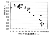
図2は積層型太陽電池の開放電圧を示し、図3は積層型太陽電池のフィルファクターを示す。
【0020】
ボロンガラス層の膜厚が50nm以下であれば、積層型太陽電池の開放電圧は、図2に示すように、第一と第二光電変換ユニットの間に特別な中間層を形成 しなくても、最大値に対して97%以上の特性を保つことができる。
また、上記膜厚が50nm以下であれば、積層型太陽電池のフィルファクターも図3に示すように良好な状態を保つことができる。これは、第一光電変換ユ ニットの表面およびボロンガラス層内における光キャリア密度が十分に高く、第二光電変換ユニットとの間に電気的な障壁が生じないことに起因すると考えられる。すなわち、50nm以下のボロンガラス層を中間層として用いることによ り、第一光電変換ユニットのp型半導体層と中間層との障壁が、ボロンガラス 層の存在によって低減されると考えられる。
【0021】
一方、ボロンガラス層を構成するシリコン、ボロン、酸素原子は1nm程度の大きさをもつため、ボロンガラス層の膜厚が1nm以下になると、均一なボロンガラス層を形成することが困難となる。また、実際に1nm以下の膜厚を測定することも事実上困難である。
【0022】
このように、第一光電変換ユニットの受光面側に形成したp型半導体層上の ボロンガラス層の膜厚が1nm〜50nmであれば、開放電圧、フィルファクターともに最大値の97%以上の特性を安定して得ることができ、中間電極層を用いることなく、低コストで安定して高効率な積層型太陽電池を得ることができるのである。
さらに、ボロンガラス層の膜厚が1nm〜20nmであれば、開放電圧は最大値の98%以上の特性を安定して得ることができる。
【0023】
ボロンガラス層のボロン濃度は、5×1019cm-3〜2×1022cm-3に制御することが好ましく、より好ましくは、1×1020cm-3〜1×1022cm-3である。これにより、積層型太陽電池の効率を高く保ちつつ、ボロンガラス層の膜厚や不純物濃度を適度に制御することが容易になる。
すなわち、通常、ボロンが含まれたシリコンは非常に活性な状態となり、不純物が取り込まれやすく、ボロンガラス層の膜厚や不純物濃度の制御が困難となるが、ボロン濃度を2×1022cm-3以下に抑えることで、第一光電変換ユニット表面の安定性を向上させることができる。
一方、ボロン濃度が5×1019cm-3以下になると、第一光電変換ユニットのpn接合部分での電位の傾きが十分に得られず、第一光電変換ユニットにおける変換効率が低下する。
【0024】
さらに、ボロンガラス層にハロゲン元素を含有させることで、ハロゲン元素がボロンガラス層内の酸素サイトに置換されることでキャリアが発生し、ハロゲン元素が存在しないときよりも、ボロンガラス層での接触抵抗が低減され、積層型太陽電池のフィルファクターを向上させることができる。
このようなハロゲン元素としては、臭素、塩素が例示される。
ボロンガラス層におけるハロゲン元素の濃度は、1×1017cm-3〜1×1019cm-3が好ましい。
【0025】
ボロンガラス層が表面に形成された第一光電変換ユニットに積層される第二光電変換ユニットは、非晶質シリコンからなる。非晶質シリコンは、結晶シリコンよりも光学的バンドギャップが高く、さらに結晶シリコンから構成される第一光電変換ユニットと同種の材料であることから、接合特性が向上する。
したがって、より高い開放電圧を得ることが可能となり、高効率化を実現することができる。
【0026】
ボロンガラス層上に形成される第二光電変換ユニットのn型半導体層は、n型ドーパントを従来の拡散手法を用いて拡散することにより形成される。n型ドーパントとしては、燐、砒素、アンチモンが挙げられる。
拡散方法としては、従来の開管法、閉管法、真空法等が用いられる。
【0027】
なお、この発明のボロンガラス層は、ボロンガラス層のp型ドーパントであるボロンの濃度が、第一光電変換ユニットのp型半導体層のボロンの濃度よりも高いが、ボロンガラス層のn型ドーパント(例えば、燐)の濃度が、第二光電変換ユニットのn型半導体層のn型ドーパントの濃度よりも低くなるよう形成される。これは、前記の特開平11-284213 号公報に開示された高濃度ドーパント介在層とは全く異なるものである。
【0028】
【実施例】
以下、本発明の積層型太陽電池の製造方法を採用した実施例について、具体的に説明する。なお、以下の実施例は一例にすぎず、種々の変更が可能である。
【0029】
<実施例1>
図1は、本発明の積層型太陽電池の構造を示す概略図である。
タンデム型の積層型太陽電池50は、ボロンガラス層13を中間層として第一光電変換ユニット1および第二光電変換ユニット2を積層してなる。
第一光電変換ユニット1は、n型結晶系シリコン基板11上にp型結晶質シリコン層12を積層してなる。第二光電変換ユニット2は、前記ボロンガラス層13上にn型半導体層21、i型半導体層22、p型半導体層23をこの順に積層してなる。n型結晶系シリコン基板11の裏面には裏面電極10が、第二光電変換ユニット2のp型半導体層23の表面には透明電極30が、それぞれ形成されている。
【0030】
タンデム型太陽電池50の製造に際し、第一光電変換ユニット1の基板として、単結晶シリコン基板をn型結晶系シリコン基板11に用いた。
まず、n型結晶質シリコン基板11をRCA 洗浄後、10% 水酸化ナトリウム水溶液を用いてシリコン基板11の厚さが400 μm になるまでエッチングを行い、混酸により350 μm までエッチングを行った。p型結晶質シリコン層12は、BBr3を用いたボロンの拡散によって形成した。ボロン拡散時のシリコン層12の拡散温度は950 ℃であった。
【0031】
このとき、ボロンが拡散されたシリコン基板11の表面にはボロンガラス層13が形成された。その後、シリコン基板11の側面と裏面側の不要なp型結晶質シリコン層およびボロンガラス層を除去した。
表面側に残存するボロンガラス層13の膜厚は約50nmであった。また、ボロンガラス層13上から四探針法によって面抵抗を測定した結果、面抵抗は40Ω/ □であった。
【0032】
次いで、ボロンが拡散されたp型結晶質シリコン層12の上に酸化シリコン膜を保護膜として形成し、POCl3 を用いたリン拡散を行い、裏面側にn +型拡散層による裏面電界(BSF) 層を形成した。
その後、側面のn +型拡散層をダイサー切断により除去して第一光電変換ユニット1を形成した。
次いで、表面の酸化シリコン膜をフッ化水素酸により除去した後、裏面にTi/Pd/Agからなる裏面電極10を蒸着法により形成した。
【0033】
次に、第二光電変換ユニット2の形成方法を説明する。
第二光電変換ユニット2を構成する各半導体層21〜23は、平行平板型プラズマCVD装置を用いて形成した。上記形成にあたっては、基板となる第一光電変換ユニット1を加熱したのち、第一光電変換ユニット1とカソードの間に高周波電力を印加し、プラズマを発生させることにより目的とする非晶質シリコン薄膜を得た。具体的な形成条件を以下の表に示す。
【0034】
【表1】

以上の方法により形成した積層型太陽電池のVoc は、1.45 Vに達し、特別な中間層を用いることなく、積層型太陽電池として十分な出力電圧を得ることができた。
【0036】
<比較例1>
この例では、第一光電変換ユニット1のp型結晶質シリコン層12を形成する際に表面に形成されたボロンガラス層を完全に除去して作製した積層型太陽電池を実施例1の積層型太陽電池と比較した。
実施例1の方法で形成されたボロンガラス層13を完全に除去した積層型太陽電池100の構造概略図を図5に示す。なお、積層型太陽電池100は、ボロンガラス層13が存在しないこと以外は、図1の積層型太陽電池50と共通する構造を有するので、説明は省略する。
【0037】
積層型太陽電池100の製造においては、ボロン拡散を行った後に形成された前記ボロンガラス層に850 ℃の熱酸化処理を行い、ボロンガラス層を完全に酸化させた後、フッ化水素酸洗浄により酸化膜を除去することでボロンガラス層を完全に除去した。
なお、一般的にボロンガラス層の残存は好ましくないと考えられており、従来、ボロンガラス層はエッチングなどの方法により完全に除去されていた。
次いで、ボロンガラス層を完全に除去した第一光電変換ユニット1の上に、透明導電膜や高濃度不純物層など特別な中間電極層を設けることなく、第二光電変換ユニット2を形成した。
【0038】
形成された積層型太陽電池100の太陽電池特性と、実施例1の本発明における積層型太陽電池50との太陽電池特性の相対比較を以下の表2に示す。
なお、表2では、各特性を比較例1の値を基準値として表示する。
【0039】
【表2】
ボロンガラス層を完全に除去した比較例1の積層型太陽電池100では、二つの光電変換ユニットの相互接触部分において逆方向の太陽電池が形成されてしまい、積層型太陽電池の特性である高い開放電圧値を得ることができなかったが、ボロンガラス層13を有する実施例1の積層型太陽電池50では、開放電圧を40%以上改善することができた。
【0041】
<比較例2>
この例では、第一光電変換ユニット1にp型結晶質シリコン基板を用いて作製した積層型太陽電池を実施例1の積層型太陽電池50と比較した。
第一光電変換ユニット1にp型結晶質シリコン基板を用いて作製した積層型太陽電池200の構造概略図を図6に示す。
積層型太陽電池200では、第一光電変換ユニット1が、p型結晶質シリコン基板12上にn型結晶質シリコン層11を積層してなる。また、第二光電変換ユニット2は、前記n型結晶質シリコン層11にp型半導体層23、i型半導体層22、n型半導体層21をこの順に積層してなる。
【0042】
積層型太陽電池200は、p型とn型の積層順序が比較例1の積層型太陽電池100と逆であるが、基本的な作製方法は同様であるため、作製方法の説明は省略する。なお、n型結晶質シリコン層11は、p型結晶質シリコン基板12上に燐を拡散させて形成した。
形成された積層型太陽電池200の太陽電池特性と、実施例1の本発明における積層型太陽電池50との太陽電池特性の相対比較を以下の表3に示す。
なお、表3では、各特性を比較例2の値を基準値として表示する。
【0043】
【表3】
比較例2の場合、第一光電変換ユニット1はp型結晶質シリコン基板12上に燐を拡散させて形成したが、燐はSi/SiO2 界面において、Si中に再拡散しやすいという特徴を有し、積層型太陽電池の中間層に利用できるほど十分なリン濃度を有するリンガラス層を形成することは困難である。もちろん、拡散表面にボロンガラス層は形成されない。そのため、透明導電膜や高濃度不純物層などの特別な中間電極層を形成しないかぎり、二つの光電変換素子の相互接触部分において逆方向の太陽電池が形成されてしまう。したがって、積層型太陽電池として機能せず、高い開放電圧を得ることはできなかった。
【0045】
実施例1、比較例1および比較例2から明らかなように、ボロン拡散工程により第一光電変換ユニットの表面に形成されるボロンガラス層を中間層として用いることで、積層型太陽電池の諸特性を高めることができる。
【0046】
<実施例2>
この例では、第一光電変換ユニット1のn型結晶質シリコン層11にボロン拡散を施した後、シリコン層11の側面および裏面側の不要なボロン拡散層およびボロンガラス層を除去する際、シリコン層11の表面側のボロンガラス層13も同時にエッチングを行うことにより、ボロンガラス層13の膜厚を変化させ、膜厚の異なる数種類の積層型太陽電池50を得た。
このようにして得られた積層型太陽電池50の開放電圧とボロンガラス層13の膜厚との相関関係を図2に示す。
なお、図2において、開放電圧は最大値を基準値(1)として表示する。
【0047】
図2から明らかなように、ボロンガラス層13の膜厚が50nm以下であれば、開放電圧は最大値に対して、97%以上の特性を保つことができることが分かる。これは、第一光電変換ユニット1の表面における光キャリア密度が十分に高く、第二光電変換ユニット2との間の電気的な障壁が低減されるためと考えられる。
【0048】
また、得られた積層型太陽電池50のフィルファクター(FF)と、第一光電変換ユニット1の表面の面抵抗との相関関係を図3に示す。なお、FFは最大値を基準値(1)として表示する。
図3から明らかなように、ボロンガラス層13の膜厚が50nm以下であれば、FFも良好な状態を保つことができる。
【0049】
<実施例3>
この例では、第一光電変換ユニット1のp型半導体層12をボロンの拡散により作製する際、ボロン拡散時のシリコン層12の拡散温度を1000℃としてボロンガラス層13中のボロン濃度が高いサンプルを作製した点で実施例1と異なる(実施例1の拡散温度は950 ℃) 。
このように作製した積層型太陽電池51と実験例1の積層型太陽電池50とを、2次イオン質量分析法(SIMS)によるボロンガラス層13中の不純物濃度測定結果で比較した。
実施例1および実施例3のサンプルについてボロン濃度と酸素濃度に関するSIMS分析を行った結果を図4に示す。
【0050】
図4において、ボロンガラス層13と第二光電変換ユニット2との界面を深さ方向の原点として表示した。なお、実施例3の積層型太陽電池の特性を、実施例1の特性を基準値(1)として表示する。
前記積層型太陽電池51は、積層型太陽電池50に比較して、開放電圧は0.95倍、FFは0.59倍であった。
【0051】
図4に示すように、実施例1のサンプルにおけるボロンガラス層13中のボロン濃度は1×1022cm-3であり、ボロンガラス層13の膜厚は約50nmであることが分かる。
一方、実施例3のサンプルにおいては、ボロンガラス層中のボロン濃度が2×1022cm-3に達し、ボロンガラス層の膜厚も100nm程度に達していた。これは、ボロン濃度の増加とともにシリコンの反応性が高まり、ボロンガラス層がより形成されやすくなり、それにともなって制御が困難になったことを意味する。
【0052】
以上の結果から、第一光電変換ユニット1の表面であるボロンガラス層13 のボロン濃度を2×1022cm-3以下に制御することによって、積層型太陽電池の効率を高く保ちつつ、ボロンガラス層の膜厚や不純物濃度を適度に制御することが容易となる。より好ましくは、ボロンガラス層13内のボロン濃度を1×1022cm-3以下に制御することが好ましい。
【0053】
<比較例3>
比較例3では、ボロンガラス層中のハロゲン元素の有無による特性を実施例1と比較した。
比較例3における積層型太陽電池では、第一光電変換ユニットのボロン拡散 層およびボロンガラス層をBBr3の拡散により形成するのではなく、ボロンイオン打ち込み法により形成した。具体的には、実施例1と同様の方法で洗浄したn型シリコン基板に、まず、BSF 層をPOCl3 拡散法により形成した後、表面側、側面側のn+層をフッ化水素酸洗浄により除去した。
【0054】
次いで、BSF 層が形成されたシリコン基板を真空チャンバ内に設置し、室温下で、加速電圧50keVのボロンイオンを9×1015cm2 で基板表側から注入した後、950 ℃で熱処理を行い、第一光電変換ユニットを形成した。
この時点で、形成された第一光電変換ユニットのSIMS測定を行った。
SIMS測定結果では、実施例1と同レベルの膜厚、ボロン濃度を有するボロンガラス層が形成されていたが、臭素や塩素は検出限界(約1015cm-3)以下であった。
【0055】
次いで、第二光電変換ユニットを実施例1と同条件で積層して積層型太陽電池を形成した。比較例4と実施例1の特性の相対比較を表4に示す。
【0056】
【表4】
比較例3における積層型太陽電池では、実施例1の積層型太陽電池に比べてフィルファクターが約13%低下し、変換効率も同様に低下していた。
実施例1の積層型太陽電池におけるボロンガラス層では、SIMS測定により1018cm-3オーダーの塩素および臭素が検出されており、ボロンガラス層中のハロゲン元素が、特性を向上させているものと考えられる。
【0058】
【発明の効果】
本発明によれば、第一光電変換ユニットの受光面側に形成したp型半導体層上のボロンガラス層を中間層として、その上から第二光電変換ユニットをn型半導体層から順次積層して第二光電変換ユニットを構成することによって、ボロンガラス層が、第一光電変換ユニットのp型半導体層と第二光電変換ユニットのn型半導体層との接合部分で逆方向太陽電池の形成を阻止する効果を有し、なおかつ、ボロンガラス層が自然酸化膜や一般の中間電極層に比べて第一光電変換ユニットのp型半導体層との間の電気的障壁を低減する効果を有するため、高効率な積層型太陽電池を得ることができる。
【0059】
前記のボロンガラス層は、ボロンを拡散した後の拡散残存表面層を利用することで、第一と第二光電変換ユニットの間に接続のための中間電極層を特別に設 ける工程あるいは装置を必要とせず、高効率化に適した拡散プロセスを利用できるため、中間層を製造するコストが削減される。
【0060】
第二光電変換ユニットが非晶質シリコン層を含むことにより、第一光電変 換ユニットと同種の材料であることから、接合特性が良好である上に、非晶質シリコンは結晶シリコンよりも光学的バンドギャップが高いことから、積層型太陽電池としてより高い開放電圧を得ることが可能となり、高効率化を実現することができる。
膜厚が1nm〜50nmであるようなボロンガラス層の上に、第二光電変換ユニットを積層することにより、安定して高効率な積層型太陽電池を得ることができる。
【0061】
ボロンガラス層のボロン濃度を、5×1019cm-3〜2×1022cm-3に制御することによって、積層型太陽電池の効率を高く保ちつつ、ボロンガラス層の膜厚や不純物濃度を適度に制御することが可能となる。
ボロンガラス層内にハロゲン元素を含有させることで、ボロンガラス層部分での接触抵抗が低減され、積層型太陽電池のFFを向上させることができる。
【図面の簡単な説明】
【図1】本発明の実施例1における積層型太陽電池の基本構造を示す概略図である。
【図2】本発明の積層型太陽電池における開放電圧とボロンガラス層の膜厚との関係を示すグラフである。
【図3】本発明の積層型太陽電池におけるフィルファクターとボロンガラス層の膜厚との関係を示すグラフである。
【図4】本発明の実施例3における積層型太陽電池のSIMS分析の結果である。
【図5】本発明の比較例1における積層型太陽電池の基本構造を示す概略図である。
【図6】本発明の比較例2における積層型太陽電池の基本構造を示す概略図である。
【図7】従来の中間層を用いた積層型太陽電池の基本構造を示す概略図である。
【符号の説明】
1 第一光電変換ユニット
2 第二光電変換ユニット
10 裏面電極
11 n型結晶質シリコン
12 p型結晶質シリコン層
13 ボロンガラス層
20 中間電極層
21 n型半導体層
22 i型半導体層
23 p型半導体層
30 透明電極層
40 集電極
50 積層型太陽電池
51 積層型太陽電池[0001]
BACKGROUND OF THE INVENTION
The present invention relates to a stacked solar cell, and more particularly to a stacked solar cell in which a plurality of photoelectric conversion units having different energy gaps are stacked and a method for manufacturing the same.
[0002]
[Prior art]
In order to effectively convert light in a wide wavelength range into electrical energy and to obtain high conversion efficiency, research and development of stacked solar cells in which two or more photoelectric conversion units with different energy gaps are stacked are widely conducted. .
When stacking the photoelectric conversion units, the photoelectric conversion unit with the smallest energy gap is arranged as the first photoelectric conversion unit on the back side of the light irradiation side so as to effectively absorb the light, and the large energy gap is set on the light irradiation side. Arrange two photoelectric conversion units.
[0003]
In the silicon-based solar cell, the first photoelectric conversion unit is mainly a photoelectric conversion unit including an amorphous silicon thin film, a microcrystalline silicon thin film, a silicon germanium thin film, or a crystalline silicon substrate as a constituent element. As the second photoelectric conversion unit, a photoelectric conversion unit including an amorphous silicon carbide thin film or an amorphous silicon thin film as a constituent element is mainly used.
[0004]
[Problems to be solved by the invention]
In general, by simply laminating the pin unit structure of a silicon solar cell as a photoelectric conversion unit, a solar cell in the opposite direction is formed at the junction between the pin unit structures, so that sufficient solar cell characteristics cannot be obtained. Therefore, in order to make the junction between the pin unit structures ohmic junction, it is necessary to form an intermediate layer acting as an electrode at the junction.
[0005]
FIG. 7 is a schematic view showing a general structure of a conventional stacked solar cell.
In the tandem
The first
[0006]
A method of using such an intermediate layer for the joint is disclosed in, for example, Japanese Patent Application Laid-Open No. 11-284213.
In the above publication, each dopant forming the p-type and n-type semiconductor layers is added to the reverse junction region at the interface between the p-type semiconductor layer and the n-type semiconductor layer in the reverse junction region where the first and second photoelectric conversion layers are adjacent to each other. An intermediate electrode layer containing a higher concentration than the dopant concentration of each of the p-type semiconductor layer and the n-type semiconductor layer is formed.
However, the above prior art requires a separate intermediate layer forming step in addition to the step of forming a plurality of pin unit structures. In order to obtain higher photoelectric conversion efficiency, each layer is formed by a plasma CVD apparatus. Therefore, it is impossible to avoid an increase in cost due to an increase in the number of chambers.
[0007]
Japanese Patent Publication No. 6-44638 discloses that an amorphous unit cell made of an amorphous semiconductor is stacked on a crystalline unit cell of an amorphous semiconductor heterojunction with a crystalline semiconductor. A technique for avoiding cancellation of electromotive force at the interface is disclosed.
In the above technology, the electromotive force of both unit elements is formed at the interface between both unit elements simply by laminating the unit cell of the crystalline photovoltaic element and the unit cell of the amorphous photovoltaic element. This is because the problem of being canceled out by the internal potential of the pn junction is taken into consideration.
However, the technique described in the above Japanese Patent Publication No. 6-44638 cannot use a diffusion process that has been established as a method for forming a crystalline photovoltaic device, and a crystalline photovoltaic formed by a diffusion process. It is difficult to form a crystalline photovoltaic element that exceeds the efficiency of the element.
Further, even if the junction characteristics at the interface portion can be improved, it is difficult to put it to practical use as a stacked solar cell having a sufficiently high conversion efficiency as a whole.
[0008]
The present invention has been made in view of the above-mentioned problems, and by improving the intermediate layer of stacked photoelectric conversion units, a stacked solar cell having high photoelectric conversion efficiency and a simplified manufacturing process. It is an object of the present invention to provide a battery and a manufacturing method thereof.
[0009]
[Means for Solving the Problems]
According to this invention, in the stacked solar cell formed by stacking a plurality of photoelectric conversion units having at least different energy gaps, the p-type semiconductor layer of the first photoelectric conversion unit and the n of the second photoelectric conversion unit on the light receiving surface side. A laminated solar cell is provided in which a boron glass layer is interposed as an intermediate layer between the first semiconductor layer and the second semiconductor layer.
[0010]
According to another aspect of the present invention, when a plurality of photoelectric conversion units having different energy gaps are sequentially stacked toward the light receiving surface side, boron is formed as a first photoelectric conversion unit on the n-type crystalline silicon substrate at a high temperature. A p-type semiconductor layer and a boron glass layer on the surface thereof are diffused, and then a second photoelectric conversion unit is sequentially laminated on the boron glass layer from the n-type semiconductor layer. A method for producing a stacked solar cell is provided.
[0011]
That is, the inventors of the present invention have conducted repeated experiments on the configuration of an intermediate electrode layer (hereinafter referred to as an intermediate layer) that serves as a stacking interface between photoelectric conversion units in a stacked solar cell. When a p-type semiconductor layer is formed by diffusing boron in an n-type crystalline silicon substrate as a unit, a boron glass layer is actively formed on the surface of the p-type semiconductor layer on the surface where boron is diffused. The present inventors have found a technique of using the boron glass layer formed as an intermediate layer with the p-type semiconductor layer, and have reached the present invention.
[0012]
Conventionally, the boron has been diffused into the silicon substrate as a p-type dopant, and the boron glass layer remaining on the surface of the silicon substrate after the diffusion of boron has been removed as degrading the characteristics of the solar cell.
An object of the present invention is to positively utilize a boron glass layer, which has been conventionally unnecessary, as an intermediate layer. Therefore, it is not necessary to use a separate process or a separate apparatus for forming the intermediate layer, and a stacked solar cell can be formed by a low-cost and simplified process.
[0013]
The boron glass layer used as the intermediate layer of the stacked solar cell of the present invention is a junction between the p-type semiconductor layer of the first photoelectric conversion unit and the n-type semiconductor layer of the second photoelectric conversion unit. Has the effect of preventing the formation of.
Furthermore, the boron glass layer can reduce an electrical barrier with the p-type semiconductor layer of the first photoelectric conversion unit due to the presence of boron, as compared with a natural oxide film or a conventional intermediate layer.
By these effects, the laminated solar cell of the present invention becomes a highly efficient laminated solar cell having good electrical junction characteristics.
[0014]
DETAILED DESCRIPTION OF THE INVENTION
Embodiments of the stacked solar cell of the present invention will be described below, but the present invention is not limited to these, and various modifications can be made.
The stacked solar cell in the present invention includes a tandem solar cell in which two photoelectric conversion units are stacked or a multi-stacked solar cell in which three or more are stacked.
[0015]
In the stacked solar cell of the present invention, the first photoelectric conversion unit is formed on the back side of the light irradiation surface (opposite to the light irradiation), and the second or further third photoelectric conversion unit is formed on the light irradiation side of the first photoelectric conversion unit. It is the laminated body which formed the conversion unit in order. The stacking position of the first and second photoelectric conversion units in the multi-stacked solar cell is not particularly limited.
The stacked solar cell according to the present invention is formed by stacking a plurality of photoelectric conversion units having at least different energy gaps, and these photoelectric conversion units have a unit structure having a pn or pin junction. In the battery, it is sufficient that the boron glass layer of the present invention is formed on at least one of the intermediate layers serving as a joint portion between the photoelectric conversion units.
Therefore, hereinafter, a tandem solar cell in which the boron glass layer is formed in the intermediate layer between the first photoelectric conversion unit and the second photoelectric conversion unit will be described as an example. The energy gap between the first and second photoelectric conversion units preferably has a difference of about 0.6 to 0.8 eV.
[0016]
The first photoelectric conversion unit in this invention is formed on an n-type crystalline silicon substrate.
The silicon substrate may be a single crystal silicon substrate or a polycrystalline silicon substrate.
Examples of the n-type dopant include phosphorus, arsenic, and antimony.
[0017]
The p-type semiconductor layer of the first photoelectric conversion unit is formed on an n-type crystalline silicon substrate in which the n-type dopant is diffused. This p-type semiconductor layer is formed by a conventional diffusion method using boron as a p-type dopant.
As a diffusion source of boron, B 2 H 6 (Gas), BBr Three (Liquid), B 2 O Three (Solid) or the like is used. As the diffusion method, a conventional open tube method, closed tube method, vacuum method, or the like is used.
In this invention, the boron glass layer is B (boron) oxide. 2 O Three SiO 2 SiO added to 2 A film is formed together with the p-type semiconductor layer when the p-type semiconductor layer is formed.
Below, the formation process of a boron glass layer is demonstrated by illustration.
For example, a liquid diffusion source (BBr Three First, the surface of the n-type crystalline silicon substrate is oxidized by oxygen gas flowing simultaneously with the diffusion source, and boron oxide is deposited on the silicon surface. After that, from the boron oxide film layer formed on the silicon substrate surface, 2B 2 O Three + 3Si → 4B + 3SiO 2 Boron atoms are introduced into the silicon substrate by this reduction reaction.
[0018]
Here, the boron concentration in the oxide film is 10 19 cm -3 When the temperature is extremely high as described above, the melting point of the boron oxide film is lowered to 1000 ° C. or lower, and a so-called “melt-through phenomenon” occurs in which the underlying oxide film having a low boron concentration is dissolved.
With this melt-through phenomenon, the diffusion of boron rapidly proceeds, and at the same time, oxygen, hydrogen, nitrogen, carbon, bromine, chlorine, fluorine, etc. present in the diffusion atmosphere are mixed into the film. As a result, a boron glass layer mainly composed of boron, silicon, and oxygen is formed.
[0019]
The boron glass layer is formed such that the p-type semiconductor layer of the first photoelectric conversion unit is formed by boron diffusion, and the boron glass layer remaining on the surface of the first photoelectric conversion unit is 1 nm to 50 nm.
The film thickness of the boron glass layer on which the boron glass layer is formed will be described with reference to FIGS.
FIG. 2 shows the open circuit voltage of the stacked solar cell, and FIG. 3 shows the fill factor of the stacked solar cell.
[0020]
If the film thickness of the boron glass layer is 50 nm or less, the open circuit voltage of the stacked solar cell does not require a special intermediate layer between the first and second photoelectric conversion units as shown in FIG. The characteristic of 97% or more with respect to the maximum value can be maintained.
Moreover, if the said film thickness is 50 nm or less, the fill factor of a laminated solar cell can also maintain a favorable state as shown in FIG. This is considered to be due to the fact that the optical carrier density in the surface of the first photoelectric conversion unit and in the boron glass layer is sufficiently high, and no electrical barrier is generated between the second photoelectric conversion unit. That is, by using a boron glass layer of 50 nm or less as the intermediate layer, it is considered that the barrier between the p-type semiconductor layer and the intermediate layer of the first photoelectric conversion unit is reduced by the presence of the boron glass layer.
[0021]
On the other hand, since silicon, boron, and oxygen atoms constituting the boron glass layer have a size of about 1 nm, it becomes difficult to form a uniform boron glass layer when the film thickness of the boron glass layer is 1 nm or less. It is also practically difficult to actually measure a film thickness of 1 nm or less.
[0022]
Thus, when the film thickness of the boron glass layer on the p-type semiconductor layer formed on the light-receiving surface side of the first photoelectric conversion unit is 1 nm to 50 nm, the open circuit voltage and the fill factor have characteristics of 97% or more of the maximum values. Thus, it is possible to obtain a highly efficient stacked solar cell at low cost without using an intermediate electrode layer.
Furthermore, if the film thickness of the boron glass layer is 1 nm to 20 nm, the open circuit voltage can stably obtain a characteristic of 98% or more of the maximum value.
[0023]
The boron concentration of the boron glass layer is 5 × 10 19 cm -3 ~ 2x10 twenty two cm -3 And more preferably 1 × 10 20 cm -3 ~ 1x10 twenty two cm -3 It is. This makes it easy to moderately control the film thickness and impurity concentration of the boron glass layer while keeping the efficiency of the stacked solar cell high.
That is, normally, silicon containing boron is in a very active state, and impurities are easily taken in, and it is difficult to control the film thickness and impurity concentration of the boron glass layer, but the boron concentration is 2 × 10. twenty two cm -3 By suppressing to the following, the stability of the surface of the first photoelectric conversion unit can be improved.
On the other hand, the boron concentration is 5 × 10. 19 cm -3 If it becomes below, the inclination of the electric potential in the pn junction part of a 1st photoelectric conversion unit will not fully be obtained, but the conversion efficiency in a 1st photoelectric conversion unit will fall.
[0024]
Furthermore, by adding a halogen element to the boron glass layer, carriers are generated by substituting the halogen element with oxygen sites in the boron glass layer, and contact with the boron glass layer is more than when no halogen element is present. The resistance is reduced, and the fill factor of the stacked solar cell can be improved.
Examples of such a halogen element include bromine and chlorine.
The concentration of the halogen element in the boron glass layer is 1 × 10 17 cm -3 ~ 1x10 19 cm -3 Is preferred.
[0025]
The second photoelectric conversion unit laminated on the first photoelectric conversion unit having the boron glass layer formed on the surface is made of amorphous silicon. Amorphous silicon has an optical band gap higher than that of crystalline silicon, and further, since it is the same kind of material as the first photoelectric conversion unit made of crystalline silicon, the junction characteristics are improved.
Therefore, a higher open circuit voltage can be obtained, and high efficiency can be realized.
[0026]
The n-type semiconductor layer of the second photoelectric conversion unit formed on the boron glass layer is formed by diffusing an n-type dopant using a conventional diffusion method. Examples of the n-type dopant include phosphorus, arsenic, and antimony.
As the diffusion method, a conventional open tube method, closed tube method, vacuum method, or the like is used.
[0027]
The boron glass layer of the present invention has a boron concentration that is the p-type dopant of the boron glass layer higher than the boron concentration of the p-type semiconductor layer of the first photoelectric conversion unit, but the n-type dopant of the boron glass layer. It is formed so that the concentration of (for example, phosphorus) is lower than the concentration of the n-type dopant of the n-type semiconductor layer of the second photoelectric conversion unit. This is completely different from the high-concentration dopant intervening layer disclosed in JP-A-11-284213.
[0028]
【Example】
Hereinafter, the Example which employ | adopted the manufacturing method of the laminated solar cell of this invention is described concretely. The following embodiment is merely an example, and various modifications can be made.
[0029]
<Example 1>
FIG. 1 is a schematic view showing the structure of the stacked solar cell of the present invention.
The tandem stacked
The first
[0030]
In manufacturing the tandem
First, after the RCA cleaning of the n-type crystalline silicon substrate 11, etching was performed using a 10% aqueous sodium hydroxide solution until the thickness of the silicon substrate 11 became 400 μm, and etching was performed to 350 μm with a mixed acid. The p-type crystalline silicon layer 12 is made of BBr Three It was formed by boron diffusion using The diffusion temperature of the silicon layer 12 during boron diffusion was 950 ° C.
[0031]
At this time, a boron glass layer 13 was formed on the surface of the silicon substrate 11 in which boron was diffused. Thereafter, unnecessary p-type crystalline silicon layer and boron glass layer on the side surface and the back surface side of the silicon substrate 11 were removed.
The boron glass layer 13 remaining on the surface side had a thickness of about 50 nm. Further, as a result of measuring the sheet resistance from above the boron glass layer 13 by the four-probe method, the sheet resistance was 40Ω / □.
[0032]
Next, a silicon oxide film is formed as a protective film on the p-type crystalline silicon layer 12 in which boron is diffused, and POCl Three Phosphorus diffusion using was performed to form a back surface electric field (BSF) layer with an n + -type diffusion layer on the back surface side.
Thereafter, the n + -type diffusion layer on the side surface was removed by dicer cutting to form the first
Next, after removing the silicon oxide film on the surface with hydrofluoric acid, a
[0033]
Next, a method for forming the second
Each semiconductor layer 21-23 which comprises the 2nd
[0034]
[Table 1]
The Voc of the stacked solar cell formed by the above method reached 1.45 V, and a sufficient output voltage as a stacked solar cell could be obtained without using a special intermediate layer.
[0036]
<Comparative Example 1>
In this example, the laminated solar cell produced by completely removing the boron glass layer formed on the surface when forming the p-type crystalline silicon layer 12 of the first
FIG. 5 shows a schematic structural diagram of the stacked
[0037]
In the production of the stacked
In general, it is considered that the remaining boron glass layer is not preferable, and conventionally, the boron glass layer has been completely removed by a method such as etching.
Next, the second
[0038]
Table 2 below shows a relative comparison between the solar cell characteristics of the formed stacked
In Table 2, each characteristic is displayed using the value of Comparative Example 1 as a reference value.
[0039]
[Table 2]
In the stacked
[0041]
<Comparative example 2>
In this example, a stacked solar cell manufactured using a p-type crystalline silicon substrate for the first
FIG. 6 shows a schematic structural diagram of a stacked
In the stacked
[0042]
In the stacked
Table 3 below shows a relative comparison between the solar cell characteristics of the formed stacked
In Table 3, each characteristic is displayed using the value of Comparative Example 2 as a reference value.
[0043]
[Table 3]
In the case of Comparative Example 2, the first
[0045]
As is clear from Example 1, Comparative Example 1 and Comparative Example 2, various properties of the stacked solar cell can be obtained by using the boron glass layer formed on the surface of the first photoelectric conversion unit by the boron diffusion process as an intermediate layer. Can be increased.
[0046]
<Example 2>
In this example, after boron diffusion is performed on the n-type crystalline silicon layer 11 of the first
FIG. 2 shows the correlation between the open-circuit voltage of the laminated
In FIG. 2, the open circuit voltage is displayed with the maximum value as the reference value (1).
[0047]
As can be seen from FIG. 2, when the thickness of the boron glass layer 13 is 50 nm or less, the open circuit voltage can maintain 97% or more of the maximum value. This is presumably because the optical carrier density on the surface of the first
[0048]
FIG. 3 shows the correlation between the fill factor (FF) of the obtained stacked
As is apparent from FIG. 3, if the boron glass layer 13 has a film thickness of 50 nm or less, the FF can also be kept in a good state.
[0049]
<Example 3>
In this example, when the p-type semiconductor layer 12 of the first
The laminated solar cell 51 produced in this way and the laminated
FIG. 4 shows the results of SIMS analysis regarding the boron concentration and oxygen concentration of the samples of Example 1 and Example 3.
[0050]
In FIG. 4, the interface between the boron glass layer 13 and the second
The laminated solar cell 51 had an open circuit voltage 0.95 times and an FF 0.59 times that of the laminated
[0051]
As shown in FIG. 4, the boron concentration in the boron glass layer 13 in the sample of Example 1 is 1 × 10. twenty two cm -3 It can be seen that the film thickness of the boron glass layer 13 is about 50 nm.
On the other hand, in the sample of Example 3, the boron concentration in the boron glass layer is 2 × 10. twenty two cm -3 And the film thickness of the boron glass layer reached about 100 nm. This means that the reactivity of silicon increases with an increase in boron concentration, and a boron glass layer is more easily formed, and accordingly, control becomes difficult.
[0052]
From the above results, the boron concentration of the boron glass layer 13 which is the surface of the first
[0053]
<Comparative Example 3>
In Comparative Example 3, the characteristics depending on the presence or absence of a halogen element in the boron glass layer were compared with Example 1.
In the stacked solar cell in Comparative Example 3, the boron diffusion layer and the boron glass layer of the first photoelectric conversion unit are made of BBr. Three It was formed by the boron ion implantation method, not by the diffusion of. Specifically, first, a BSF layer is put on POCl on an n-type silicon substrate cleaned in the same manner as in Example 1. Three After the formation by the diffusion method, the n + layer on the surface side and side surface side was removed by hydrofluoric acid cleaning.
[0054]
Next, the silicon substrate on which the BSF layer is formed is placed in a vacuum chamber, and boron ions having an acceleration voltage of 50 keV are applied at 9 × 10 at room temperature. 15 cm 2 After injecting from the substrate front side, heat treatment was performed at 950 ° C. to form a first photoelectric conversion unit.
At this time, the SIMS measurement of the formed first photoelectric conversion unit was performed.
In the SIMS measurement results, a boron glass layer having the same film thickness and boron concentration as in Example 1 was formed, but bromine and chlorine were detected at a detection limit (about 10 15 cm -3 )
[0055]
Next, the second photoelectric conversion unit was stacked under the same conditions as in Example 1 to form a stacked solar cell. Table 4 shows a relative comparison of characteristics between Comparative Example 4 and Example 1.
[0056]
[Table 4]
In the laminated solar cell in Comparative Example 3, the fill factor was reduced by about 13% compared to the laminated solar cell in Example 1, and the conversion efficiency was similarly lowered.
In the boron glass layer in the laminated solar cell of Example 1, 10 was measured by SIMS measurement. 18 cm -3 Ordered chlorine and bromine have been detected, and it is considered that the halogen element in the boron glass layer has improved the characteristics.
[0058]
【The invention's effect】
According to the present invention, the boron glass layer on the p-type semiconductor layer formed on the light receiving surface side of the first photoelectric conversion unit is used as an intermediate layer, and the second photoelectric conversion unit is sequentially stacked from the n-type semiconductor layer thereon. By forming the second photoelectric conversion unit, the boron glass layer prevents the formation of a reverse solar cell at the junction between the p-type semiconductor layer of the first photoelectric conversion unit and the n-type semiconductor layer of the second photoelectric conversion unit. In addition, the boron glass layer has an effect of reducing an electrical barrier between the p-type semiconductor layer of the first photoelectric conversion unit as compared with a natural oxide film or a general intermediate electrode layer. An efficient stacked solar cell can be obtained.
[0059]
The boron glass layer uses a diffusion remaining surface layer after diffusing boron, thereby providing a process or apparatus for specially providing an intermediate electrode layer for connection between the first and second photoelectric conversion units. The cost for manufacturing the intermediate layer is reduced because a diffusion process suitable for high efficiency can be used without being required.
[0060]
Since the second photoelectric conversion unit includes an amorphous silicon layer, it is the same material as the first photoelectric conversion unit, so that the bonding characteristics are good and amorphous silicon is more optical than crystalline silicon. Since the target band gap is high, a higher open circuit voltage can be obtained as a stacked solar cell, and high efficiency can be realized.
By laminating the second photoelectric conversion unit on the boron glass layer having a film thickness of 1 nm to 50 nm, a highly efficient laminated solar cell can be obtained.
[0061]
The boron concentration of the boron glass layer is 5 × 10 19 cm -3 ~ 2x10 twenty two cm -3 By controlling the thickness, the film thickness and impurity concentration of the boron glass layer can be appropriately controlled while keeping the efficiency of the stacked solar cell high.
By containing a halogen element in the boron glass layer, the contact resistance in the boron glass layer portion is reduced, and the FF of the stacked solar cell can be improved.
[Brief description of the drawings]
FIG. 1 is a schematic diagram showing a basic structure of a stacked solar cell in Example 1 of the present invention.
FIG. 2 is a graph showing the relationship between the open circuit voltage and the thickness of a boron glass layer in the stacked solar cell of the present invention.
FIG. 3 is a graph showing the relationship between the fill factor and the boron glass layer thickness in the stacked solar cell of the present invention.
FIG. 4 is a result of SIMS analysis of the stacked solar cell in Example 3 of the present invention.
FIG. 5 is a schematic view showing the basic structure of a stacked solar cell in Comparative Example 1 of the present invention.
FIG. 6 is a schematic view showing a basic structure of a stacked solar cell in Comparative Example 2 of the present invention.
FIG. 7 is a schematic diagram showing the basic structure of a conventional stacked solar cell using an intermediate layer.
[Explanation of symbols]
1 First photoelectric conversion unit
2 Second photoelectric conversion unit
10 Back electrode
11 n-type crystalline silicon
12 p-type crystalline silicon layer
13 Boron glass layer
20 Intermediate electrode layer
21 n-type semiconductor layer
22 i-type semiconductor layer
23 p-type semiconductor layer
30 Transparent electrode layer
40 Current collector
50 stacked solar cells
51 stacked solar cells
Claims (7)
Priority Applications (1)
| Application Number | Priority Date | Filing Date | Title |
|---|---|---|---|
| JP2000398428A JP4185246B2 (en) | 2000-12-27 | 2000-12-27 | Laminated solar cell and method for manufacturing the same |
Applications Claiming Priority (1)
| Application Number | Priority Date | Filing Date | Title |
|---|---|---|---|
| JP2000398428A JP4185246B2 (en) | 2000-12-27 | 2000-12-27 | Laminated solar cell and method for manufacturing the same |
Publications (2)
| Publication Number | Publication Date |
|---|---|
| JP2002198552A JP2002198552A (en) | 2002-07-12 |
| JP4185246B2 true JP4185246B2 (en) | 2008-11-26 |
Family
ID=18863401
Family Applications (1)
| Application Number | Title | Priority Date | Filing Date |
|---|---|---|---|
| JP2000398428A Expired - Fee Related JP4185246B2 (en) | 2000-12-27 | 2000-12-27 | Laminated solar cell and method for manufacturing the same |
Country Status (1)
| Country | Link |
|---|---|
| JP (1) | JP4185246B2 (en) |
Families Citing this family (4)
| Publication number | Priority date | Publication date | Assignee | Title |
|---|---|---|---|---|
| JP5509414B2 (en) * | 2010-01-28 | 2014-06-04 | 大日本スクリーン製造株式会社 | Solar cell evaluation apparatus and solar cell evaluation method |
| JP2011216586A (en) * | 2010-03-31 | 2011-10-27 | Sharp Corp | Laminated photoelectric conversion device and method of manufacturing the same |
| JP2015138959A (en) * | 2014-01-24 | 2015-07-30 | 三菱電機株式会社 | Photovoltaic device and photovoltaic device manufacturing method |
| CN116364787A (en) * | 2021-12-22 | 2023-06-30 | 中国科学院宁波材料技术与工程研究所 | Interfacial composite structure and its preparation method and application of two-terminal tandem solar cell |
-
2000
- 2000-12-27 JP JP2000398428A patent/JP4185246B2/en not_active Expired - Fee Related
Also Published As
| Publication number | Publication date |
|---|---|
| JP2002198552A (en) | 2002-07-12 |
Similar Documents
| Publication | Publication Date | Title |
|---|---|---|
| CN115241298A (en) | Solar cell and preparation method thereof, photovoltaic module | |
| US8658458B2 (en) | Patterned doping for polysilicon emitter solar cells | |
| KR101000064B1 (en) | Heterojunction solar cell and its manufacturing method | |
| JP2009164544A (en) | Passivation layer structure of solar cell and manufacturing method thereof | |
| KR101225978B1 (en) | Sollar Cell And Fabrication Method Thereof | |
| JP5626361B2 (en) | SOLAR CELL, SOLAR CELL MODULE, AND SOLAR CELL MANUFACTURING METHOD | |
| JP2010521824A (en) | Solar cell | |
| KR101886818B1 (en) | Method for manufacturing of heterojunction silicon solar cell | |
| TWI424582B (en) | Solar cell manufacturing method | |
| AU2024391414A1 (en) | Topcon cell, and topcon cell preparation method | |
| KR102148427B1 (en) | Photoelectric device and the manufacturing method thereof | |
| KR101543767B1 (en) | Method for forming selective emitter of solar cell, and solar cell and manufacturing method thereof | |
| KR102547804B1 (en) | Bifacial silicon solar cell and method for manufacturing the same | |
| JP2014011246A (en) | Solar cell element and solar cell module | |
| US11251315B2 (en) | Solar cells with improved lifetime, passivation and/or efficiency | |
| CN105190864A (en) | Monolithic semi-conductor substrate based on silicon, divided into sub-cells | |
| JP4185246B2 (en) | Laminated solar cell and method for manufacturing the same | |
| CN119133292B (en) | Solar cell and photovoltaic module | |
| JP5645734B2 (en) | Solar cell element | |
| JP2675754B2 (en) | Solar cell | |
| CN115036398B (en) | A method for preparing a P-type silicon solar cell | |
| JP5975841B2 (en) | Manufacturing method of photovoltaic device and photovoltaic device | |
| CN119069548A (en) | Solar cell and preparation method thereof, photovoltaic module | |
| CN114695583B (en) | Solar cell, production method and photovoltaic module | |
| CN117810308A (en) | Preparation method of solar cell, solar cell and photovoltaic module |
Legal Events
| Date | Code | Title | Description |
|---|---|---|---|
| A621 | Written request for application examination |
Free format text: JAPANESE INTERMEDIATE CODE: A621 Effective date: 20061024 |
|
| A977 | Report on retrieval |
Free format text: JAPANESE INTERMEDIATE CODE: A971007 Effective date: 20080827 |
|
| TRDD | Decision of grant or rejection written | ||
| A01 | Written decision to grant a patent or to grant a registration (utility model) |
Free format text: JAPANESE INTERMEDIATE CODE: A01 Effective date: 20080902 |
|
| A01 | Written decision to grant a patent or to grant a registration (utility model) |
Free format text: JAPANESE INTERMEDIATE CODE: A01 |
|
| A61 | First payment of annual fees (during grant procedure) |
Free format text: JAPANESE INTERMEDIATE CODE: A61 Effective date: 20080905 |
|
| FPAY | Renewal fee payment (event date is renewal date of database) |
Free format text: PAYMENT UNTIL: 20110912 Year of fee payment: 3 |
|
| R150 | Certificate of patent or registration of utility model |
Free format text: JAPANESE INTERMEDIATE CODE: R150 |
|
| FPAY | Renewal fee payment (event date is renewal date of database) |
Free format text: PAYMENT UNTIL: 20120912 Year of fee payment: 4 |
|
| FPAY | Renewal fee payment (event date is renewal date of database) |
Free format text: PAYMENT UNTIL: 20130912 Year of fee payment: 5 |
|
| LAPS | Cancellation because of no payment of annual fees |