JP4198770B2 - Data input circuit and data input method for semiconductor memory device - Google Patents
Data input circuit and data input method for semiconductor memory device Download PDFInfo
- Publication number
- JP4198770B2 JP4198770B2 JP33327397A JP33327397A JP4198770B2 JP 4198770 B2 JP4198770 B2 JP 4198770B2 JP 33327397 A JP33327397 A JP 33327397A JP 33327397 A JP33327397 A JP 33327397A JP 4198770 B2 JP4198770 B2 JP 4198770B2
- Authority
- JP
- Japan
- Prior art keywords
- signal
- data
- pulse
- input
- output signal
- Prior art date
- Legal status (The legal status is an assumption and is not a legal conclusion. Google has not performed a legal analysis and makes no representation as to the accuracy of the status listed.)
- Expired - Fee Related
Links
Images




Classifications
-
- G—PHYSICS
- G11—INFORMATION STORAGE
- G11C—STATIC STORES
- G11C7/00—Arrangements for writing information into, or reading information out from, a digital store
- G11C7/10—Input/output [I/O] data interface arrangements, e.g. I/O data control circuits, I/O data buffers
- G11C7/1078—Data input circuits, e.g. write amplifiers, data input buffers, data input registers, data input level conversion circuits
- G11C7/1093—Input synchronization
-
- G—PHYSICS
- G11—INFORMATION STORAGE
- G11C—STATIC STORES
- G11C11/00—Digital stores characterised by the use of particular electric or magnetic storage elements; Storage elements therefor
- G11C11/21—Digital stores characterised by the use of particular electric or magnetic storage elements; Storage elements therefor using electric elements
- G11C11/34—Digital stores characterised by the use of particular electric or magnetic storage elements; Storage elements therefor using electric elements using semiconductor devices
- G11C11/40—Digital stores characterised by the use of particular electric or magnetic storage elements; Storage elements therefor using electric elements using semiconductor devices using transistors
- G11C11/401—Digital stores characterised by the use of particular electric or magnetic storage elements; Storage elements therefor using electric elements using semiconductor devices using transistors forming cells needing refreshing or charge regeneration, i.e. dynamic cells
- G11C11/4063—Auxiliary circuits, e.g. for addressing, decoding, driving, writing, sensing or timing
- G11C11/407—Auxiliary circuits, e.g. for addressing, decoding, driving, writing, sensing or timing for memory cells of the field-effect type
- G11C11/4076—Timing circuits
-
- G—PHYSICS
- G11—INFORMATION STORAGE
- G11C—STATIC STORES
- G11C7/00—Arrangements for writing information into, or reading information out from, a digital store
- G11C7/10—Input/output [I/O] data interface arrangements, e.g. I/O data control circuits, I/O data buffers
- G11C7/1078—Data input circuits, e.g. write amplifiers, data input buffers, data input registers, data input level conversion circuits
- G11C7/1084—Data input buffers, e.g. comprising level conversion circuits, circuits for adapting load
-
- G—PHYSICS
- G11—INFORMATION STORAGE
- G11C—STATIC STORES
- G11C7/00—Arrangements for writing information into, or reading information out from, a digital store
- G11C7/22—Read-write [R-W] timing or clocking circuits; Read-write [R-W] control signal generators or management
- G11C7/222—Clock generating, synchronizing or distributing circuits within memory device
-
- G—PHYSICS
- G11—INFORMATION STORAGE
- G11C—STATIC STORES
- G11C7/00—Arrangements for writing information into, or reading information out from, a digital store
- G11C7/22—Read-write [R-W] timing or clocking circuits; Read-write [R-W] control signal generators or management
- G11C7/225—Clock input buffers
Landscapes
- Engineering & Computer Science (AREA)
- Microelectronics & Electronic Packaging (AREA)
- Computer Hardware Design (AREA)
- Dram (AREA)
- Static Random-Access Memory (AREA)
Description
【0001】
【発明の属する技術分野】
本発明は半導体メモリ装置のデータ入力回路及びデータ入力方法に係り、特に反響クロック発生器を具備してクロックサイクル周期を短縮する同期式半導体メモリ装置のデータ入力回路及びデータ入力方法に関する。
【従来の技術】
一般に、コンピュータシステムは与えられた作業に対する命令を行うための中央処理装置(CPU)と、CPUが要求するデータ、プログラムを格納するための主メモリとを有している。したがって、コンピュータシステムの性能向上のためには、CPUの動作速度を向上させることと、CPUが待機時間無しに動作して主メモリへのアクセス時間をできるだけ縮めることが要求される。このような要求によりシステムクロックの制御を受けて動作し、主メモリへのアクセス時間が著しく縮められた同期式DRAM(SDRAM)が出現するようになった。
【0002】
通常、SDRAMはシステムクロックの遷移により発生するパルス信号に応答して動作が制御されることを特徴とする。ところが、クロックに同期して動作する同期式半導体メモリ装置において、クロックサイクルタイム(tCC)は多様な要素により制限される。
【0003】
すなわち、tCC(CLOCK CYCLE TIME)の限界はメモリとデータ制御部に入力されるクロックの所要時間の差(以下、tSWという)、クロック同期からデータ出力までの所要時間(以下、tACという)、データがメモリから制御部まで伝達される時間(以下、tFLという)、制御部でのデータセットアップ時間(以下、tSSという)等の和により決定される。
【0004】
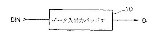
図1は従来の技術におけるデータ入出力回路のブロック図を示した図面であり、外部から入力されるデータは単に入力バッファ10を経てメモリ装置に入力されることがわかる。
【0005】
また図2は、従来の技術においてtCCの限界を招く各種所要時間を示した図面である。ここで、CLK_SYSはシステムクロックの波形を、CLK_CNTRは制御部に入力されるクロックの波形を、CLK_DRAMはDRAMに入力されるクロックの波形を、DATA_DRAMはDRAMから出力されるデータを、DATA_CNTRは制御部から発生するデータを各々示す。
【0006】
【発明が解決しようとする課題】
上記従来のSDRAMにおいては、図2を参照すると、システム上でtCCは、tSW、tAC,tFL及びtSSの和よりも大きくなければならないという限界を有することが分かる。従って、従来のデータ入出力回路では例えば300MHz以上の周波数を有するSDRAMを実現することは不可能であった。
本発明は前記の目的を達成するために案出されたものであり、クロックのサイクル時間を短縮可能な半導体メモリ装置のデータ入力回路及びデータ入力方法を提供することを目的とする。
【課題を解決するための手段】
前記目的を達成するために本発明の半導体メモリ装置のデータ入力回路は、半導体メモリ装置において、入力データと同一のタイミングで入力されるデータクロック信号に基づいて発生する反響クロック信号に同期して、前記入力データを前記半導体メモリ装置に入力することを特徴とする。
例えば、前記データクロック信号のパルス数をカウントして指定された数に到るまでパルスを発生する反響クロック発生器と、前記反響クロック発生器により発生されるパルスに同期して前記入力データを前記半導体メモリ装置に伝送する入力データ伝送手段と、を具備することを特徴とする。
【発明の実施の形態】
以下、本発明に係る一実施形態について、添付した図面に基づき詳細に説明する。尚、各図面において同一の参照符号は同一の構成要素を表す。
【0007】
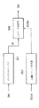
図3は、本実施形態の反響クロック発生器を有するデータ入力回路を示すブロック図である。同図によれば、本実施形態の半導体メモリ装置のデータ入出力回路は、データ入力バッファ301、反響クロック発生器303及び入力データ伝送部305から構成される。
【0008】
データ入力バッファ301は外部から入力される入力データDINをバッファリングする。また、反響クロック発生器303は外部データクロックDCLKの数が指定された数に到るまで、外部データクロックDCLKの遷移に応答してパルスを発生する。また、入力データ伝送部305は反響クロック発生器303の出力信号XCONのパルスに応答してデータ入力バッファ301の出力信号DIを伝送する。
【0009】
図4は、図3に示す入力データ伝送部305の詳細構成を示した図である。同図によれば、入力データ伝送部305は第1反転バッファ401、伝送ゲート403及び第2反転バッファ405等から構成される。第1反転バッファ401はデータ入力バッファ301の出力信号をバッファリングして反転させる。そして、伝送ゲート403の一端には反響クロック発生器303の出力信号XCONが入力され、他端には第3反転バッファ407を経て反転されたXCONが入力され、その入力パルスに応答して第1反転バッファ401の出力信号(N402)を伝送する。かつ、前記第2反転バッファ405は伝送ゲート403により伝送された第1反転バッファ401の出力信号(N402)をバッファリングして反転させる。
【0010】
従って、外部データクロックDCLKの遷移が発生する度に、反響クロック発生器303の出力信号であるXCONはパルスを発生するようになる。よって、入力データ伝送部305の伝送ゲート403が“ターンオン”されて、データ入力バッファ301の出力信号DIをメモリチップの内部に伝送する。ところで、前記反響クロック発生器303は外部データクロックDCLKの数が外部システムにより決定された所定数に至ると、パルスの発生を中止する。よって、入力データDINは外部システムで決定した所定数のみが、チップの内部に入力される。
【0011】
図5は、本実施形態のデータ入力回路における反響クロック発生器303の詳細構成を示した図である。同図によれば、反響クロック発生器303は反響クロックバッファ501、反響パルス発生部503、バスト長カウンタ505、ラッチ部507及びリセットパルス発生部509から構成される。
【0012】
反響クロックバッファ501は外部データクロック信号DCLKをバッファリングしてXPULを出力する。そして、反響パルス発生部503は所定のパルスイネーブル信号PULENによりイネーブルされ、反響クロックバッファ501の出力信号XPULの遷移に応答して自身の出力信号XCONパルスを発生する。また、バスト長カウンタ505は所定のリセットパルスRESETにより先充電され、反響パルス発生部503から発生する出力信号XCONのパルス数が指定された数に一致する時に、自身の出力信号BLCNTが遷移される。
【0013】
尚、ラッチ部507はリセットパルスRESETにより先充電され、反響クロックバッファ501の出力信号XPULの最初の遷移によりラッチされ、バスト長カウンタ505の出力信号BLCNTの遷移によりラッチが解除されるパルスイネーブル信号PULENを発生する。以下、ラッチ部507の構成を更に具体的に説明する。
ラッチ部507は第1論理和反転部511及び第2論理和反転部513を具備する。前記第1論理和反転部511は、前記DCLKに応答する信号XPULと第2論理和反転部513の出力VPREを入力信号とする。そして、第2論理和反転部513はバスト長カウンタ505の出力信号BLCNTと第1論理和反転部513の出力信号(N512)を入力信号とする。
以下、ラッチ部507の動作を説明する。ラッチ部507の動作初期においては、バスト長カウンタ505の出力信号BLCNTは“ロー”状態である。すると、反響クロックバッファ501の出力信号XPULが“ハイ”に遷移されると、第1論理和反転部511の出力(N512)は“ロー”状態になり、第2論理和反転部513の出力信号VPREは“ハイ”状態にラッチされる。従って、後に反響クロックバッファ501の出力信号XPULが引き続き遷移されても、ラッチ部507の出力信号PULENの論理状態は遷移されなくなる。
【0014】
そして、反響パルス発生部503で指定された数のパルス、すなわちデータバスト長分のパルスが発生すると、バスト長カウンタ505の出力信号BLCNTが“ハイ”に遷移される。すると、反響クロックバッファ501の出力信号XPULが“ロー”になる時、ラッチ部507の出力信号PULENが“ロー”になり、反響パルス発生部503の出力信号XCONはパルスを発生しなくなる。
そして、リセットパルス発生部509はパルスイネーブル信号PULENの遷移に応答してリセットパルスRESETを発生する。ここで、本実施形態のラッチ部507はラッチ解除部515を具備する。ラッチ解除部515はパワーアップ(POWER−UP)やリセット(RESET)パルスが発生する際に、第2論理和反転部513の出力信号VPREのラッチを解除する。
【0015】
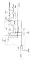
図6は、図5に示した反響クロックバッファ501の詳細構成例を示す図である。同図によれば、本実施形態の反響クロックバッファ501は、下位電流ミラー601、上位電流ミラー603及びラッチ部605から構成される。下位電流ミラー601は所定の下位基準電圧VRLを基準として、データクロックDCLKの電圧をバッファリングする。また、上位電流ミラー603は下位基準電圧VRLより高い所定の上位基準電圧VRHを基準として、データクロックDCLKの電圧をバッファリングする。また、ラッチ部605は下位電流ミラー601の出力信号(N602)を第1入力信号とし、上位電流ミラー603の出力信号(N604)を第2入力信号とする。尚、反響クロックバッファ501の出力信号であるXPULは、データクロック信号DCLKのレベルが下位基準電圧VRL以下に下降する場合、及びデータクロック信号DCLKのレベルが上位基準電圧VRH以上に上昇する場合に、遷移される。
【0016】
下位電流ミラー601は、プルアップトランジスタ607、第1PMOSトランジスタ609、第2PMOSトランジスタ611、第1NMOSトランジスタ613及び第2NMOSトランジスタ615から構成される。プルアップトランジスタ607はそのソースが電源電圧VCCに接続され、所定の反響クロックイネーブル信号XENがアクティブ時にインバータ628を経てロー信号として入力され、ターンオンされる。そして、第1PMOSトランジスタ609はそのソースがプルアップトランジスタ607のドレインに接続され、そのゲートに下位基準電圧VRLが印加される。また、第2PMOSトランジスタ611はそのソースが前記プルアップトランジスタ607のドレインに接続され、そのゲートにデータクロック信号DCLKが印加される。そして、第1NMOSトランジスタ613はそのソースが接地電圧VSSに接続され、そのゲートとドレインが第1PMOSトランジスタ609のドレインに共通接続される共通接続点(N610)を有する。また、第2NMOSトランジスタ615はそのソースが接地電圧VSSに接続され、そのゲートは共通接続点(N610)に接続され、そのドレインは第2PMOSトランジスタ611のドレインに共通接続されて、下位電流ミラーの出力信号(N602)を発生する。
【0017】
従って、前記XENが“ハイ”にイネーブルされると、下位電流ミラー601はデータクロック信号DCLKに応答する。データクロック信号DCLKのレベルが下位基準電圧VRLより高い場合には、第1PMOSトランジスタ609のゲートとソースとの電圧Vgsが第2PMOSトランジスタ611のVgsより大きくなる。従って、端子N610の電圧が上昇して、第2NMOSトランジスタ615の影響が第2PMOSトランジスタ611の影響よりも大きくなる。よって、下位電流ミラー601の出力端子N602の電圧はVSS側に下降するようになる。
【0018】
一方、データクロック信号DCLKのレベルが下位基準電圧VRLより低い場合には、第1PMOSトランジスタ609のVgsが第2PMOSトランジスタ611のVgsより小さくなる。従って、共通接続点(N610)の電圧が下降し、第2NMOSトランジスタ615の影響が第2PMOSトランジスタ611の影響より小さくなる。よって、下位電流ミラー601の出力端子N602の電圧はVCCの方に上昇するようになる。
【0019】
下位電流ミラー601は、そのソースが接地電圧VSSに接続され、そのドレインは下位電流ミラー601の出力(N602)に接続され、反響クロックイネーブル信号XENがディスエーブルされる時に“ターンオン”される第3NMOSトランジスタ617を更に具備する。従って、XENが“ロー”にディスエーブルされると、第3NMOSトランジスタ617は“ターンオン”されて下位電流ミラー601の出力端子(N602)のレベルはVSSにセットされる。また、XENが“ハイ”にイネーブルされると、第3NMOSトランジスタ617は“ターンオフ”されて下位電流ミラー601の出力端子(N602)のセッティグが解除される。
【0020】
上位電流ミラー603は、プルダウントランジスタ619、第4NMOSトランジスタ621、第5NMOSトランジスタ623、第3PMOSトランジスタ625及び第4PMOSトランジスタ627から構成される。プルダウントランジスタ619はそのソースが接地電圧VSSに接続され、所定の反響クロックイネーブル信号XENがアクティブされる時にターンオンされる。そして、第4NMOSトランジスタ621はそのソースが前記プルダウントランジスタ619のドレインに接続され、そのゲートに上位基準電圧VRHが印加される。また、第5NMOSトランジスタ623はそのソースがプルダウントランジスタ619のドレインに接続され、そのゲートにデータクロック信号DCLKが印加される。そして、第3PMOSトランジスタ625はそのソースが電源電圧VCCに接続され、そのゲートとドレインが第4NMOSトランジスタ621のドレインに共通接続される共通接続点(N622)を有する。また、第4PMOSトランジスタ627はそのソースが電源電圧VCCに接続され、そのゲートが共通接続点(N622)に接続され、そのドレインが第5NMOSトランジスタ623のドレインに共通接続されて上位電流ミラー603の出力信号(N604)を発生する。
【0021】
従って、XENが“ハイ”にイネーブルされると、上位電流ミラー603はデータクロック信号DCLKに応答する。データクロック信号DCLKのレベルが上位基準電圧VRHより低い場合には、第5NMOSトランジスタ621のVgsが第5NMOSトランジスタ623のVgsより大きくなる。よって、共通接続点(N622)の電圧が下降して、第3PMOSトランジスタ627の影響が第5NMOSトランジスタ623の影響より大きくなる。よって、上位電流ミラー603の出力端子N604の電圧はVCCの方に上昇するようになる。
一方、データクロック信号DCLKのレベルが上位基準電圧VRHより高い場合には、第4NMOSトランジスタ621のVgsが第5NMOSトランジスタ623のVgsより小さくなる。従って、共通接続点(N622)の電圧が上昇して、第3PMOSトランジスタ627の影響が第5NMOSトランジスタ623の影響より小さくなる。よって、上位電流ミラー603の出力端子N604の電圧はVSSの方に下降するようになる。
【0022】
上位電流ミラー603は、そのソースが電源電圧VCCに接続され、そのドレインが上位電流ミラー603の出力(N604)に接続され、反響クロックイネーブル信号XENがディスエーブルされる時に“ターンオン”される第5PMOSトランジスタ629を更に具備する。従って、XENが“ロー”にディスエーブルされると、第5PMOSトランジスタ629は“ターンオン”されて上位電流ミラー603の出力端子(N604)のレベルがVCCにセットされる。また、XENが“ハイ”にイネーブルされると、第5PMOSトランジスタ629は“ターンオフ”されて上位電流ミラー603の出力端子(N604)のセッティンが解除される。
【0023】
ラッチ部605は、反転部631、第1論理積反転部633、第2論理積反転部635及び反転バッファ637を具備する。反転部631は、下位電流ミラー601の出力信号(N602)のレベルを反転させる。そして第1論理積反転部633は、反転部631の出力信号(N632)を第1入力信号とする。また、第2論理積反転部635は上位電流ミラー603の出力信号(N604)と第1論理積反転部633の出力信号(N634)の論理積をとって反転させ、その出力信号(N636)を前記第1論理積反転部633の第2入力信号とする。そして、反転バッファ637は第1論理積反転部633の出力信号(N634)を反転かつバッファリングして、反響クロックバッファ501の出力信号XPULを発生する。
【0024】
以上の構成により、データクロック信号DCLKのレベルが下位基準電圧VRLより低くなる場合には、下位電流ミラー601の出力信号(N602)のレベルが上昇する。かつ、反転部631の出力信号(N632)のレベルは“ロー”になり、反響クロックバッファ501の出力信号XPULのレベルは“ロー”に下降するようになる。この際、上位電流ミラー603の出力信号(N604)のレベルは“ハイ”になり、第2論理積反転部635の出力信号(N636)の論理状態は“ロー”になる。
【0025】
また、データクロック信号DCLKのレベルが“下位基準電圧VRL以下”から“VRLとVRHの間の電圧”に上昇する場合、下位電流ミラー601の出力信号(N602)のレベルは下降するようになる。従って、反転部631の出力信号(N632)のレベルは“ハイ”になる。ところが、第2論理積反転部635の出力信号(N636)の論理状態は“ロー”を保つので、反響クロックバッファ501の出力信号XPULのレベルは変わらなくなる。
また、データクロック信号DCLKのレベルが上位基準電圧VRHより高くなる場合には、下位電流ミラー601の出力信号(N602)のレベルは下降するようになる。そして、反転部631の出力信号(N632)のレベルは“ハイ”になる。この際、上位電流ミラー603の出力信号(N604)のレベルは“ロー”になり、第2論理積反転部635の出力信号(N636)の論理状態は“ハイ”になる。よって、反響クロックバッファ501の出力信号XPULのレベルは“ハイ”に上昇するようになる。
【0026】
また、データクロック信号DCLKのレベルが“前記上位基準電圧VRH以上”から“VRLとVRHの間の電圧”に下降する場合、上位電流ミラー603の出力信号(N604)のレベルは上昇するようになる。ところが、第1論理積反転部633の出力信号(N634)の論理状態は“ロー”を保つので、第2論理積反転部635の出力信号(N636)の論理状態は引き続き“ハイ”状態を保つ。よって、反響クロックバッファ501の出力信号XPULのレベルは変わらなくなる。
【0027】
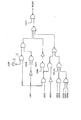
次に図7に、図5に示した反響パルス発生部503の詳細構成を示す。同図によれば、反響パルス発生部503は反転遅延部701、第1論理積部703、論理和反転部705、論理和部707及び第2論理積部709から構成される。反転遅延部701は、反響クロックバッファ501の出力信号XPULを反転して遅延させる。そして、第1論理積部703は反響クロックバッファ501の出力信号XPULと、反転遅延部701の出力信号(N702)の論理積をとる。そして論理和反転部705は、反響クロックバッファ501の出力信号XPULと反転遅延部701の出力信号(N702)との論理和をとって反転させる。そして、論理和部707は第1論理積部703の出力信号(N704)と論理和反転部705の出力信号(N706)を論理和をとる。また、第2論理積部709はパルスイネーブル信号PULENによりイネーブルされ、論理和部707の出力信号(N708)に応答して、XCON信号を出力する。図8は、信号XPULの遷移に応じる図7の反響パルス発生部503の主要端子におけるタイミングチャートである。同図を参照して反響パルス発生部503の動作を説明すると、信号XPULの論理状態が“ハイからローに”又は“ローからハイに”遷移される度に、論理和部707の出力信号(N708)はパルスとして発生される。従って、パルスイネーブル信号PULENの論理状態が“ハイ”である時には、反響パルス発生部503の出力信号XCONは論理和部707の出力信号(N708)の遷移に応答して同じくパルスとして発生される。ところが、パルスイネーブル信号PULENの論理状態が“ロー”である時には、反響パルス発生部503はパルスを発生しない。図9は、図5のリセットパルス発生部509の詳細構成を示す図である。リセットパルス発生部509は、指定された数、すなわちデータバスト長だけのクロック信号が入力される時、リセットパルスを発生する。図9を参照して説明すると、リセットパルス発生部509は反転遅延部901、論理和反転部903及び論理和部905から構成される。反転遅延部901はパルスイネーブル信号PULENを反転遅延させる。そして、論理和反転部903はパルスイネーブル信号PULENと反転遅延部901の出力信号(N902)を入力信号とする。従って、パルスイネーブル信号PULENの論理状態が“ハイ”から“ロー”に遷移する度に、論理和反転部903の出力信号(N904)は“ロー”から“ハイ”へのパルスが発生する。そして、論理和部905はパワーアップ時にパルスが発生するパワーアップ信号VCCHBと、論理和反転部903の出力信号(N904)を入力信号とする。従って、パワーアップ時やPULENの論理状態が“ハイ”から“ロー”に遷移する時に、論理和部905の出力信号であるリセット信号RESETはパルスとして発生される。図10は、図5のバスト長カウンタ505の詳細構成を示した図面である。同図によれば、バスト長カウンタ505はカウンティング信号発生部1001及びバスト信号発生部1003から構成される。カウンティング信号発生部1001は、反響パルス発生部503から発生する出力信号XCONのパルス数を測定してその出力信号であるカウンティング信号群CNT0〜CNT8を発生する。バスト信号発生部1003は、該カウンティング信号群を受けてバスト長を表す信号BLCNTを発生する。図11は、図10のカウンティング信号発生部1001の詳細構成を示した図面である。同図を参照すると、カウンティング信号発生部1001はA型カウンタ1101及びB型カウンタ(1102,1103,…)から構成される。図12は、図11のA型カウンタ1101の詳細構成を示した図面である。同図によれば、A型カウンタ1101は論理和反転部1201、第1及び第2反転部1203,1215、第1伝送ゲート1205、第1ラッチ部1207、第2伝送ゲート1209、第2ラッチ部1211及びNMOSトランジスタ1213から構成されている。論理和反転部1201は、リセットパルスRESETと反響パルス発生部503の出力信号XCONとの論理和を反転させる。そして、第1反転部1203はA型カウンタ1101の出力信号であるCNT0の論理状態を反転させる。また、第1伝送ゲート1205はリセットパルスRESETが“ロー”にディスエーブルされた状態で反響パルス発生部503の出力信号XCONが“ロー”にディスエーブルされる時、第1反転部1203の出力信号(N1204)を伝送する。そして、第1ラッチ部1207は第1伝送ゲート1205により伝送された信号をラッチさせる。また、第2伝送ゲート1209はリセットパルスRESETが“ハイ”にイネーブルされるかXCONが“ハイ”にイネーブルされる時、第1ラッチ部1207の出力信号(N1208)を伝送する。尚、第2ラッチ部1211は第2伝送ゲート1207により伝送された信号をラッチさせる。そして、NMOSトランジスタ1213はそのソースが接地電圧VSSに接続され、リセットパルスRESETによりゲートされて第1ラッチ部1207の入力端子(N1206)をVSSに先充電させる。
【0028】
以上の構成からなるA型カウンタ1101の動作について、以下に説明する。まず、リセットパルスRESETが“ハイ”にアクティブされると、NMOSトランジスタ1213が“ターンオン”される。よって、第1ラッチ部1207の入力端子(N1206)はVSSに先充電される。そして、第2伝送ゲート1209は“ターンオン”され、A型カウンタ1101の出力信号CNT0の論理状態は“ロー”である。また、第1反転部1203の出力信号(N1204)は“ハイ”であり、第1伝送ゲート1205は“ターンオフ”される。そして、リセットパルスRESETが“ロー”にディスエーブルされると、NMOSトランジスタ1213が“ターンオフ”される。また、第1伝送ゲート1205は“ターンオン”され、第1ラッチ部1207の出力信号(N1208)の論理状態は“ロー”になる。この際、第2伝送ゲート1209は“ターンオフ”されている。そして、反響パルス発生部503の出力信号XCONが“ハイ”にアクティブされる時、第2伝送ゲート1209が“ターンオン”され、A型カウンタ1101の出力信号CNT0の論理状態は“ハイ”に遷移される。また、反響パルス発生部503の出力信号XCONが“ロー”にディスエーブルされる時、第1伝送ゲート1209が“ターンオン”されて第1ラッチ部1207の出力信号(N1208)の論理状態が遷移される。このように、反響パルス発生部503の出力信号XCONがパルスを形成する度に、A型カウンタ1101の出力信号CNT0の論理状態は遷移を繰り返すようになる。
図13は、図11のB型カウンタ(1102,1103,…)の詳細構成を示した図面である。同図を参照すると、図12に示されたA型カウンタ1101とほとんど類似しているが、やや異なる点もある。即ち、A型カウンタ1101の論理和反転部1201はリセットパルスRESETと反響パルス発生部503の出力信号XCONを入力信号としたが、B型カウンタ(1102,1103,…)の論理和反転部1301はリセットパルスRESETと反響パルス発生部503の出力信号XCON、及び前段階のカウンタの出力信号の論理状態を表す信号CARRYBi-1を入力信号としている。前段階のカウンタの出力信号の論理状態がすべて“ハイ”である時のみに、信号CARRYBi-1の論理状態が“ロー”になる。また、信号CARRYBi-1の論理状態が“ロー”である時、B型カウンタはA型カウンタと同様に動作するようになる。
【0029】
上述した図12のA型カウンタと図13のB型カウンタを参照して、図11のカウンティング信号発生部1001の動作を以下に説明する。まず、リセットパルスRESETによりリセット動作が行われると、A型カウンタ1101とB型カウンタ(1102,1103,…)の出力信号であるCNT0〜CNT8がすべて“0”に先充電される。そして、信号XCONが一番目のパルスを発生すると、CNT0の論理状態が“1”になる。かつ、信号XCONが二番目のパルスを発生すると、CNT0の論理状態は“0”になり、CNT1の論理状態が“1”になる。尚、信号XCONが三番目のパルスを発生すると、CNT0の論理状態は再び“1”になる。そして、信号XCONが四番目のパルスを発生すると、CNT0とCNT1の論理状態は“0”になり、CNT2の論理状態が“1”になる。このように、信号XCONがパルスを発生する度に、カウンティング信号発生部1001の出力信号であるCNT0〜CNT8が順次変換され、信号XCONのパルスを測定するようになる。また、XCONが指定された数だけパルスを発生するようになると、リセット信号RESETがアクティブされて信号CNT0〜CNT8がすべて“0”に先充電される。
図14は、図10のバスト長カウンタ505のバスト信号発生部1003を示した図面である。バスト信号発生部1003は、カウンティング信号群CNT0〜CNT8に応答して、反響パルス発生部503から発生する出力信号XCONのパルス数が指定入力パルス数に一致する時に遷移される出力信号BLCNTを発生する。
図14に示すSZ2Bは、入力データのバスト長が2以上である場合に“ハイ”になる信号である。そして、SZ4Bは入力データのバスト長が4以上である場合に“ハイ”になる信号であり、SZ8Bは入力データのバスト長が8以上である場合に“ハイ”になる信号である。また、SZFULLは入力データのバスト長がFULLである場合に“ハイ”になる信号である。
ここで、例えば入力データのバスト長が4である場合を仮定すると、この場合、SZ2BとSZ4Bは“ハイ”であり、SZ8BとSZFULLは“ロー”である。この際、反響パルス発生部503から発生する出力信号XCONの四番目のパルスが発生すると、CNT2が“ハイ”になり残りのカウンティング信号群CNT0,CNT1,CNT3〜CNT8は“ロー”になる。この際、出力信号BLCNTの論理状態は“ロー”から“ハイ”に遷移されるようになる。
【0030】
以上説明したように本実施形態に示す反響クロック発生器を具備したデータ入力回路においては、データ入力時に反響クロック発生器303で指定された数、すなわちデータバスト長に応答してパルスを発生させる。そして、反響クロック発生器303のパルスを用いて、データ入力バッファ301を経て入力された外部データDINを半導体メモリチップの内部に伝送する。
【0031】
従って、データの入力時、クロック同期からデータの出力までかかる時間(データアクセスタイム)tAC及びデータがメモリから制御部まで伝送される時間tFLの影響を排除して、同期式半導体メモリ装置のデータアクセス動作速度を改善することができる。
【0032】
尚、本発明は本実施形態に限られず、本発明が属した技術的思想内で当分野において通常の知識を有する者により、多くの変形が可能であることは明らかである。
【発明の効果】
以上説明したように、本発明による反響クロック発生器を具備したデータ入力回路によれば、クロックサイクルタイムtCCに対して、クロック同期からデータの出力までかかる時間tAC及びデータがメモリから制御部まで伝送されるにかかる時間tFLの影響を排除することができるため、半導体メモリ装置のクロックのサイクル時間tCCを短縮することができ、データアクセス動作速度を改善することができる。
【0033】
【図面の簡単な説明】
【図1】従来のデータ入出力回路構成を示すブロック図である。
【図2】従来のクロックサイクルタイムを決定するタイミングチャートである。
【図3】本発明に係る一実施形態における反響クロック発生器を有するデータ入力回路の構成を示すブロック図である。
【図4】本実施形態における入力データ伝送部の詳細構成を示すブロック図である
【図5】本実施形態における反響クロック発生器の詳細構成を示すブロック図である。
【図6】本実施形態における反響クロックバッファの詳細構成を示すブロック図である。
【図7】本実施形態における反響パルス発生部の詳細構成を示すブロック図である。
【図8】本実施形態における反響パルス発生部の主要端子のタイミングチャートである。
【図9】本実施形態におけるリセットパルス発生部の詳細構成を示すブロック図である。
【図10】本実施形態におけるバスト長カウンタの詳細構成を示すブロック図である。
【図11】本実施形態におけるカウンティング信号発生部の詳細構成を示すブロック図である。
【図12】本実施形態におけるA型カウンタの詳細構成を示すブロック図である。
【図13】本実施形態におけるB型カウンタの詳細構成を示すブロック図である。
【図14】本実施形態におけるバスト信号発生部の詳細構成を示すブロック図である。
【符号の説明】
301 データ入力バッファ
303 反響クロック発生器
305 データ伝送部
501 反響クロックバッファ
503 反響パルス発生部
505 バスト長カウンタ
509 リセットパルス発生部[0001]
BACKGROUND OF THE INVENTION
The present invention relates to a data input circuit and a data input method of a semiconductor memory device, and more particularly, to a data input circuit and a data input method of a synchronous semiconductor memory device having an echo clock generator to shorten a clock cycle period.
[Prior art]
Generally, a computer system has a central processing unit (CPU) for executing instructions for a given work, and a main memory for storing data and programs required by the CPU. Therefore, in order to improve the performance of the computer system, it is required that the operation speed of the CPU is improved and that the CPU operates without waiting time to shorten the access time to the main memory as much as possible. In response to such a demand, a synchronous DRAM (SDRAM) that operates under the control of the system clock and whose access time to the main memory is significantly shortened has appeared.
[0002]
In general, the SDRAM is characterized in that the operation is controlled in response to a pulse signal generated by the transition of the system clock. However, in a synchronous semiconductor memory device that operates in synchronization with a clock, the clock cycle time (tCC) is limited by various factors.
[0003]
That is, the limit of tCC (CLOCK CYCLE TIME) is the difference between the required time of the clock input to the memory and the data control unit (hereinafter referred to as tSW), the required time from clock synchronization to data output (hereinafter referred to as tAC), data Is transmitted from the memory to the control unit (hereinafter referred to as tFL), the data setup time in the control unit (hereinafter referred to as tSS), and the like.
[0004]
FIG. 1 is a block diagram of a conventional data input / output circuit, and it can be seen that data input from the outside is simply input to a memory device via an
[0005]
FIG. 2 is a diagram illustrating various required times that cause the limit of tCC in the conventional technology. Here, CLK_SYS is the waveform of the system clock, CLK_CNTR is the waveform of the clock input to the control unit, CLK_DRAM is the waveform of the clock input to the DRAM, DATA_DRAM is the data output from the DRAM, and DATA_CNTR is the control unit The data generated from is shown respectively.
[0006]
[Problems to be solved by the invention]
In the conventional SDRAM, referring to FIG. 2, it can be seen that tCC has a limit that it must be larger than the sum of tSW, tAC, tFL and tSS on the system. Therefore, it has been impossible to realize an SDRAM having a frequency of, for example, 300 MHz or more with a conventional data input / output circuit.
The present invention has been devised to achieve the above-described object, and an object thereof is to provide a data input circuit and a data input method for a semiconductor memory device capable of shortening the clock cycle time.
[Means for Solving the Problems]
In order to achieve the above object, the data input circuit of the semiconductor memory device of the present invention is synchronized with an echo clock signal generated based on a data clock signal input at the same timing as the input data in the semiconductor memory device. The input data is input to the semiconductor memory device.
For example, an echo clock generator that counts the number of pulses of the data clock signal and generates pulses until a specified number is reached, and the input data is synchronized with the pulse generated by the echo clock generator. Input data transmission means for transmitting to the semiconductor memory device.
DETAILED DESCRIPTION OF THE INVENTION
Hereinafter, an embodiment according to the present invention will be described in detail with reference to the accompanying drawings. In the drawings, the same reference numerals represent the same components.
[0007]
FIG. 3 is a block diagram showing a data input circuit having an echo clock generator according to this embodiment. As shown in the figure, the data input / output circuit of the semiconductor memory device of this embodiment includes a
[0008]
The
[0009]
FIG. 4 is a diagram showing a detailed configuration of the input
[0010]
Therefore, every time a transition of the external data clock DCLK occurs, the XCON which is the output signal of the
[0011]
FIG. 5 is a diagram showing a detailed configuration of the
[0012]
The
[0013]
Note that the
The
Hereinafter, the operation of the
[0014]
When the number of pulses designated by the
The
[0015]
FIG. 6 is a diagram showing a detailed configuration example of the
[0016]
The lower
[0017]
Therefore, when the XEN is enabled high, the lower
[0018]
On the other hand, when the level of the data clock signal DCLK is lower than the lower reference voltage VRL, Vgs of the
[0019]
The lower
[0020]
The upper
[0021]
Thus, when XEN is enabled “high”, the upper
On the other hand, when the level of the data clock signal DCLK is higher than the upper reference voltage VRH, Vgs of the
[0022]
The upper
[0023]
The
[0024]
With the above configuration, when the level of the data clock signal DCLK becomes lower than the lower reference voltage VRL, the level of the output signal (N602) of the lower
[0025]
Further, when the level of the data clock signal DCLK increases from “below the lower reference voltage VRL” to “the voltage between VRL and VRH”, the level of the output signal (N602) of the lower
In addition, when the level of the data clock signal DCLK becomes higher than the upper reference voltage VRH, the level of the output signal (N602) of the lower
[0026]
Further, when the level of the data clock signal DCLK decreases from “above the upper reference voltage VRH” to “voltage between VRL and VRH”, the level of the output signal (N604) of the upper
[0027]
Next, FIG. 7 shows a detailed configuration of the
[0028]
The operation of the
FIG. 13 is a diagram showing a detailed configuration of the B-type counters (1102, 1103,...) Of FIG. Referring to the figure, it is almost similar to the
[0029]
The operation of the
FIG. 14 shows a
SZ2B shown in FIG. 14 is a signal that goes “high” when the bust length of the input data is 2 or more. SZ4B is a signal that becomes “high” when the bust length of the input data is 4 or more, and SZ8B is a signal that becomes “high” when the bust length of the input data is 8 or more. SZFULL is a signal that goes high when the bust length of the input data is FULL.
Here, for example, assuming that the bust length of the input data is 4, in this case, SZ2B and SZ4B are “high”, and SZ8B and SZFULL are “low”. At this time, when the fourth pulse of the output signal XCON generated from the
[0030]
As described above, in the data input circuit having the echo clock generator shown in the present embodiment, pulses are generated in response to the number designated by the
[0031]
Therefore, the data access time of the synchronous semiconductor memory device is eliminated by eliminating the influence of the time (data access time) tAC from the clock synchronization to the data output at the time of data input and the time tFL during which the data is transmitted from the memory to the control unit. The operation speed can be improved.
[0032]
It should be noted that the present invention is not limited to the present embodiment, and it is obvious that many modifications are possible by those having ordinary knowledge in the art within the technical idea to which the present invention belongs.
【The invention's effect】
As described above, according to the data input circuit including the echo clock generator according to the present invention, the time tAC required from clock synchronization to data output and the data are transmitted from the memory to the control unit with respect to the clock cycle time tCC. Since the influence of the time tFL required for the operation can be eliminated, the clock cycle time tCC of the semiconductor memory device can be shortened, and the data access operation speed can be improved.
[0033]
[Brief description of the drawings]
FIG. 1 is a block diagram showing a configuration of a conventional data input / output circuit.
FIG. 2 is a timing chart for determining a conventional clock cycle time.
FIG. 3 is a block diagram showing a configuration of a data input circuit having an echo clock generator according to an embodiment of the present invention.
FIG. 4 is a block diagram showing a detailed configuration of an input data transmission unit in the present embodiment.
FIG. 5 is a block diagram showing a detailed configuration of an echo clock generator in the present embodiment.
FIG. 6 is a block diagram showing a detailed configuration of an echo clock buffer in the present embodiment.
FIG. 7 is a block diagram showing a detailed configuration of an echo pulse generator in the present embodiment.
FIG. 8 is a timing chart of main terminals of an echo pulse generator in the present embodiment.
FIG. 9 is a block diagram showing a detailed configuration of a reset pulse generator in the present embodiment.
FIG. 10 is a block diagram showing a detailed configuration of a bust length counter in the present embodiment.
FIG. 11 is a block diagram showing a detailed configuration of a counting signal generator in the present embodiment.
FIG. 12 is a block diagram showing a detailed configuration of an A-type counter in the present embodiment.
FIG. 13 is a block diagram showing a detailed configuration of a B-type counter in the present embodiment.
FIG. 14 is a block diagram showing a detailed configuration of a bust signal generator in the present embodiment.
[Explanation of symbols]
301 Data input buffer
303 echo clock generator
305 Data transmission unit
501 Echo clock buffer
503 echo pulse generator
505 Bust length counter
509 Reset pulse generator
Claims (13)
前記反響クロック信号のパルス数をカウントして指定された数に到るまでパルスを発生する反響クロック発生器と、前記反響クロック発生器により発生されるパルスに同期して前記入力データを前記半導体メモリ装置に伝送する入力データ伝送手段と、を具備することを特徴とするデータ入力回路。In a semiconductor memory device, a data input circuit for inputting the input data to the semiconductor memory device in synchronization with an echo clock signal generated based on a data clock signal input at the same timing as the input data ,
An echo clock generator that counts the number of pulses of the echo clock signal and generates pulses until a specified number is reached, and the input data is synchronized with the pulses generated by the echo clock generator in the semiconductor memory An input data transmission means for transmitting to the apparatus .
前記反響クロック信号のパルス数をカウントして指定された数に到るまでパルスを発生する反響クロック発生工程と、前記反響クロック発生工程において発生されたパルスに同期して前記入力データを前記半導体メモリ装置に伝送する入力データ伝送工程と、を備えることを特徴とするデータ入力方法。In a semiconductor memory device, a data input method for inputting the input data to the semiconductor memory device in synchronization with an echo clock signal generated based on a data clock signal input at the same timing as the input data ,
An echo clock generating step for counting the number of pulses of the echo clock signal until a specified number is reached, and the input data in synchronization with the pulses generated in the echo clock generating step An input data transmission step for transmitting to an apparatus .
Applications Claiming Priority (2)
| Application Number | Priority Date | Filing Date | Title |
|---|---|---|---|
| KR97-2885 | 1997-01-30 | ||
| KR1019970002885A KR100224687B1 (en) | 1997-01-30 | 1997-01-30 | Semiconductor memory device with echo clock receiver |
Publications (2)
| Publication Number | Publication Date |
|---|---|
| JPH10214483A JPH10214483A (en) | 1998-08-11 |
| JP4198770B2 true JP4198770B2 (en) | 2008-12-17 |
Family
ID=19496031
Family Applications (1)
| Application Number | Title | Priority Date | Filing Date |
|---|---|---|---|
| JP33327397A Expired - Fee Related JP4198770B2 (en) | 1997-01-30 | 1997-12-03 | Data input circuit and data input method for semiconductor memory device |
Country Status (3)
| Country | Link |
|---|---|
| JP (1) | JP4198770B2 (en) |
| KR (1) | KR100224687B1 (en) |
| TW (1) | TW342501B (en) |
Families Citing this family (2)
| Publication number | Priority date | Publication date | Assignee | Title |
|---|---|---|---|---|
| JP2013131277A (en) | 2011-12-22 | 2013-07-04 | Elpida Memory Inc | Semiconductor device and manufacturing method for the same |
| KR20160045270A (en) | 2014-10-17 | 2016-04-27 | 박종민 | Fishing hook assembly for catching squids |
-
1997
- 1997-01-30 KR KR1019970002885A patent/KR100224687B1/en not_active Expired - Fee Related
- 1997-09-05 TW TW086112832A patent/TW342501B/en not_active IP Right Cessation
- 1997-12-03 JP JP33327397A patent/JP4198770B2/en not_active Expired - Fee Related
Also Published As
| Publication number | Publication date |
|---|---|
| JPH10214483A (en) | 1998-08-11 |
| KR100224687B1 (en) | 1999-10-15 |
| TW342501B (en) | 1998-10-11 |
| KR19980067040A (en) | 1998-10-15 |
Similar Documents
| Publication | Publication Date | Title |
|---|---|---|
| US5920511A (en) | High-speed data input circuit for a synchronous memory device | |
| JP4322209B2 (en) | Method and apparatus for setting and compensating for read latency in high speed DRAM | |
| KR100370293B1 (en) | Cycle independent data to echo clock tracking circuit | |
| US5384735A (en) | Data output buffer of a semiconductor memory device | |
| US6064625A (en) | Semiconductor memory device having a short write time | |
| JP3979690B2 (en) | Semiconductor memory device system and semiconductor memory device | |
| US7889595B2 (en) | Semiconductor memory device | |
| KR100303775B1 (en) | Method and apparatus for controlling data strobe signal in DISD DRAM | |
| KR101879394B1 (en) | Semiconductor system and command address setup/hold time control method | |
| US5535171A (en) | Data output buffer of a semiconducter memory device | |
| KR20190112838A (en) | Apparatus and method for determining phase relationship between input clock signal and multiphase clock signal | |
| US9111607B2 (en) | Multiple data rate memory with read timing information | |
| KR19990072385A (en) | Semiconductor device reconciling different timing signals | |
| KR100883140B1 (en) | Data output control circuit, semiconductor memory device and operation method thereof | |
| US6192004B1 (en) | Semiconductor integrated circuit | |
| US7016256B2 (en) | Data input unit of synchronous semiconductor memory device, and data input method using the same | |
| KR0167683B1 (en) | Data output buffer control method for high frequency operation of synchronous memory | |
| JPH09120672A (en) | Synchronous semiconductor memory | |
| JP2000036192A (en) | Semiconductor integrated circuit | |
| JP2001093280A (en) | Semiconductor storage device | |
| JP4198770B2 (en) | Data input circuit and data input method for semiconductor memory device | |
| KR100638748B1 (en) | Semiconductor memory device | |
| US20080211551A1 (en) | Semiconductor memory device | |
| US7142467B2 (en) | Synchronous semiconductor memory device | |
| KR100748461B1 (en) | Data input circuit and method of semiconductor memory device |
Legal Events
| Date | Code | Title | Description |
|---|---|---|---|
| A621 | Written request for application examination |
Free format text: JAPANESE INTERMEDIATE CODE: A621 Effective date: 20040930 |
|
| A977 | Report on retrieval |
Free format text: JAPANESE INTERMEDIATE CODE: A971007 Effective date: 20061220 |
|
| A131 | Notification of reasons for refusal |
Free format text: JAPANESE INTERMEDIATE CODE: A131 Effective date: 20070205 |
|
| A601 | Written request for extension of time |
Free format text: JAPANESE INTERMEDIATE CODE: A601 Effective date: 20070507 |
|
| A602 | Written permission of extension of time |
Free format text: JAPANESE INTERMEDIATE CODE: A602 Effective date: 20070516 |
|
| A521 | Written amendment |
Free format text: JAPANESE INTERMEDIATE CODE: A523 Effective date: 20070524 |
|
| A131 | Notification of reasons for refusal |
Free format text: JAPANESE INTERMEDIATE CODE: A131 Effective date: 20080107 |
|
| A601 | Written request for extension of time |
Free format text: JAPANESE INTERMEDIATE CODE: A601 Effective date: 20080124 |
|
| A602 | Written permission of extension of time |
Free format text: JAPANESE INTERMEDIATE CODE: A602 Effective date: 20080129 |
|
| RD03 | Notification of appointment of power of attorney |
Free format text: JAPANESE INTERMEDIATE CODE: A7423 Effective date: 20080201 |
|
| RD04 | Notification of resignation of power of attorney |
Free format text: JAPANESE INTERMEDIATE CODE: A7424 Effective date: 20080206 |
|
| RD04 | Notification of resignation of power of attorney |
Free format text: JAPANESE INTERMEDIATE CODE: A7424 Effective date: 20080611 |
|
| A521 | Written amendment |
Free format text: JAPANESE INTERMEDIATE CODE: A523 Effective date: 20080707 |
|
| TRDD | Decision of grant or rejection written | ||
| A01 | Written decision to grant a patent or to grant a registration (utility model) |
Free format text: JAPANESE INTERMEDIATE CODE: A01 Effective date: 20080902 |
|
| A01 | Written decision to grant a patent or to grant a registration (utility model) |
Free format text: JAPANESE INTERMEDIATE CODE: A01 |
|
| A61 | First payment of annual fees (during grant procedure) |
Free format text: JAPANESE INTERMEDIATE CODE: A61 Effective date: 20081002 |
|
| FPAY | Renewal fee payment (event date is renewal date of database) |
Free format text: PAYMENT UNTIL: 20111010 Year of fee payment: 3 |
|
| R150 | Certificate of patent or registration of utility model |
Free format text: JAPANESE INTERMEDIATE CODE: R150 |
|
| FPAY | Renewal fee payment (event date is renewal date of database) |
Free format text: PAYMENT UNTIL: 20121010 Year of fee payment: 4 |
|
| FPAY | Renewal fee payment (event date is renewal date of database) |
Free format text: PAYMENT UNTIL: 20131010 Year of fee payment: 5 |
|
| R250 | Receipt of annual fees |
Free format text: JAPANESE INTERMEDIATE CODE: R250 |
|
| LAPS | Cancellation because of no payment of annual fees |