JP4200516B2 - How to remove flicker from an image - Google Patents
How to remove flicker from an image Download PDFInfo
- Publication number
- JP4200516B2 JP4200516B2 JP2002212267A JP2002212267A JP4200516B2 JP 4200516 B2 JP4200516 B2 JP 4200516B2 JP 2002212267 A JP2002212267 A JP 2002212267A JP 2002212267 A JP2002212267 A JP 2002212267A JP 4200516 B2 JP4200516 B2 JP 4200516B2
- Authority
- JP
- Japan
- Prior art keywords
- flicker
- image
- function
- image data
- energy
- Prior art date
- Legal status (The legal status is an assumption and is not a legal conclusion. Google has not performed a legal analysis and makes no representation as to the accuracy of the status listed.)
- Expired - Lifetime
Links
- 238000000034 method Methods 0.000 claims description 63
- 238000003384 imaging method Methods 0.000 description 11
- 238000005286 illumination Methods 0.000 description 7
- 230000000694 effects Effects 0.000 description 5
- OAICVXFJPJFONN-UHFFFAOYSA-N Phosphorus Chemical compound [P] OAICVXFJPJFONN-UHFFFAOYSA-N 0.000 description 4
- 238000001514 detection method Methods 0.000 description 4
- 238000010586 diagram Methods 0.000 description 4
- 230000010354 integration Effects 0.000 description 2
- 230000003287 optical effect Effects 0.000 description 2
- 230000000737 periodic effect Effects 0.000 description 2
- 238000009825 accumulation Methods 0.000 description 1
- 230000004397 blinking Effects 0.000 description 1
- 230000000295 complement effect Effects 0.000 description 1
- 238000001816 cooling Methods 0.000 description 1
- 238000003702 image correction Methods 0.000 description 1
- QSHDDOUJBYECFT-UHFFFAOYSA-N mercury Chemical compound [Hg] QSHDDOUJBYECFT-UHFFFAOYSA-N 0.000 description 1
- 229910044991 metal oxide Inorganic materials 0.000 description 1
- 150000004706 metal oxides Chemical class 0.000 description 1
- 238000012544 monitoring process Methods 0.000 description 1
- 239000004065 semiconductor Substances 0.000 description 1
Images





Classifications
-
- H—ELECTRICITY
- H04—ELECTRIC COMMUNICATION TECHNIQUE
- H04N—PICTORIAL COMMUNICATION, e.g. TELEVISION
- H04N23/00—Cameras or camera modules comprising electronic image sensors; Control thereof
- H04N23/70—Circuitry for compensating brightness variation in the scene
- H04N23/745—Detection of flicker frequency or suppression of flicker wherein the flicker is caused by illumination, e.g. due to fluorescent tube illumination or pulsed LED illumination
-
- H—ELECTRICITY
- H04—ELECTRIC COMMUNICATION TECHNIQUE
- H04N—PICTORIAL COMMUNICATION, e.g. TELEVISION
- H04N23/00—Cameras or camera modules comprising electronic image sensors; Control thereof
- H04N23/70—Circuitry for compensating brightness variation in the scene
-
- H—ELECTRICITY
- H04—ELECTRIC COMMUNICATION TECHNIQUE
- H04N—PICTORIAL COMMUNICATION, e.g. TELEVISION
- H04N23/00—Cameras or camera modules comprising electronic image sensors; Control thereof
- H04N23/80—Camera processing pipelines; Components thereof
- H04N23/81—Camera processing pipelines; Components thereof for suppressing or minimising disturbance in the image signal generation
-
- H—ELECTRICITY
- H04—ELECTRIC COMMUNICATION TECHNIQUE
- H04N—PICTORIAL COMMUNICATION, e.g. TELEVISION
- H04N25/00—Circuitry of solid-state image sensors [SSIS]; Control thereof
- H04N25/70—SSIS architectures; Circuits associated therewith
- H04N25/76—Addressed sensors, e.g. MOS or CMOS sensors
Landscapes
- Engineering & Computer Science (AREA)
- Multimedia (AREA)
- Signal Processing (AREA)
- Transforming Light Signals Into Electric Signals (AREA)
- Studio Devices (AREA)
- Picture Signal Circuits (AREA)
Description
【0001】
【発明の属する技術分野】
本発明は、概ね画像処理分野に係り、より具体的には周期的に変動する光源によって生ずる偽画像を画像から除去する方法及び装置に関する。
【0002】
【従来の技術】
CMOS(相補型金属酸化膜半導体)のアクティブ画素方式画像センサでは、露光制御に一般に回転シャッタが用いられる。回転シャッタは、画像センサ列のセンサ各行を順次リセットし、後刻各行の値を順次読み出すことで稼働する。露光期間はリセットと読出しの時間間隔に等しく、フレーム周期は配列内の各行の値を読み出すのに必要な時間となる。
【0003】
図1は、本発明を明瞭に理解して貰えるよう、回転シャッタの動作について概略図示した線図である。100行(図1には説明の便宜上9行だけを図示)を有する画像データアレイについて検討する。単一行の読み出しに必要な時間、すなわち行期間をTとし、図1の矢印10で示す露光期間をn×Tに設定したとする。行1の露光は時間t=0にて始まり、その行は時間t=n×Tで読み出される。行2の露光は時間t=Tで開始され、行2は時間t=(n+1)×Tにて読み出される。配列の行100は時間t=99×Tで露光を開始し、その行は時間t=(n+99)×Tにて読み出される。
【0004】
回転シャッタの一つの特性は、図1に示す如く、各行ごとの露光が異なる時間期間に亙って起こることである。従って、シーンの照明が時間とともに変動する場合、撮像された画像の輝度は行ごとに変動する。シーンの照度レベルにおける変動期間が回転シャッタの集積期間より長くてフレーム周期よりも短い場合、上記変動は画像内に水平帯の形で偽画像(image artifacts)が現われる結果を招く。画像内の帯の数は、フレーム周期で割ったフリッカ周期に等しい。
【0005】
光源の照度レベルにおけるこれらの時間に対する変動は、「フリッカ」として知られており、画像の水平帯は偽画像或いは「フリッカパターン」と呼ばれる。例えば、蛍光灯は非常に強いフリッカを有する。ランプの蛍光体は、電力線周波数の各ピークで励起され、ピーク間で減衰する。生成される光パルスは、交流電力線の2倍のフリッカ周波数を有する。白熱バルブはフリッカを示さないが、それはフィラメントの熱量が十分に大きく、フィラメントが交流ピーク間でかなり冷めるのを防止するからである。
【0006】
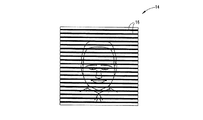
CMOS画像センサの出力へのフリッカの影響は、図2の概略画像14に例示してあり、同図では周期的な水平バー16が非常に明白であり、画像の全般的な品質を相当に損なうものである。
【0007】
図2に示したような画像内の水平バーの数は、フリッカ周期に対するフレーム周期の比に等しい。水平バーの振幅は、特定光源の特性とCMOS画像センサの回転シャッタの集積期間に依存する。
【0008】
幾つかの方法が、フレームごとのフリッカを除去するのに考案されてきた。例えば、米国特許第5,793,886号には異なる画像フレームのヒストグラムを比較し、これにより時間の関数としての平均照度の変動を取り除くようにした方法が開示されている。しかしながら、ここに記述された方法は、単一の画像フレームしか利用できず、しかもフリッカが生成画像内の一連の水平帯として明示される状況には適用し得ないのである。
【0009】
フレームごとのフリッカを取り除く他の公知の方法は、光源の輝度をフレーム露光期間中に監視するものである。例えば、米国特許第6,208,433号に記載された方法では、光源の変動監視用に別個のセンサが用いられ、このセンサの出力が画像補正に用いられる。米国特許第5,960,153号では、撮像と光源変動の計測の両方にリニア画像センサが用いられる。光源変動を露光時間制御に用い、これにより最終画像にフリッカが現われないようにしてある。
【0010】
さらに別の公知の方法では、露光期間をフリッカ周期の整数倍に制限することでフリッカを防止している。この種の状況下では、各行は光源変動の全周期の整数倍で光を集積する。その結果、集積された光レベルは各行ごとに同一となり、画像に帯が現われることはなくなる。本方法の欠点は、露光期間をフリッカ期間よりも短くできないことにある。光源が非常に明るく、露光期間が低減できない場合、生成画像は露出過多となる。この種の問題は、明るい蛍光源でシーンを照らすか、カメラを直接蛍光源へ向けたときに生ずることがある。
【0011】
【発明が解決しようとする課題】
一般に、画像からフレームごとのフリッカを除去する公知の方法は、処理用に幾つかの連続画像フレームを必要としたり、フリッカを独立に監視する必要があったり、追加の入力を必要としたりする。従って、フリッカ除去用の公知の方法は完全に満足は出来ないのである。必要なものは、単一画像上に作用する周期的に変動する光源により生成されたフリッカを除去し、フリッカ周期とフレーム周期の値を除きどんな追加の入力も必要とせず、フリッカを独立して監視する必要のない方法と装置である。同じく必要とされるのは、非常に明るい蛍光照明下でも非常に低いフリッカをもって画像を撮像することに活用できる方法と装置である。
【0012】
【課題を解決するための手段】
本発明は、蛍光源のような周期的に変動する光源により生成される画像から偽画像を除去する方法と装置を提供するものである。本発明による方法は、画像データにより表される画像から偽画像を除去するものである。本方法では、フリッカ関数を割り出し、このフリッカ関数を用いて画像データを処理して偽画像を除去する。
【0013】
本発明にあっては、撮像シーンを照明する光源の光照射をモデル化したフリッカ関数を用いて画像を処理することにより画像から偽画像を除去或いは大幅に低減できることが判った。本発明は、回転シャッタを用いてCMOS画像センサから収集した画像データにより表される画像から偽画像を除去するのに特に適したものである。
【0014】
本発明の一実施形態によれば、画像を表わす画像データは、複数行の画像データからなる画像データアレイからなり、画像データの処理ステップは、行単位ベースで画像データをフリッカ関数により除算することからなる。
【0015】
画像データのフリッカ関数の割り出しは、前以て用意したフリッカモデルに関連するパラメータ値の割り出しを含む。特に、フリッカ関数を割り出すため光源のフリッカ周波数やフリッカ振幅やフリッカ位相が割り出される。本発明の一実施形態では、フリッカ周波数とフリッカ振幅とフリッカ位相は、画像データアレイの各行沿いに画素を寄せ集めて列ベクトルを生成し、フレーム周期と画像フレームごとの交流線繰り返し周波数との積からフリッカ周波数を割り出し、補正列ベクトル内のフリッカエネルギを最小化してフリッカの振幅及び位相を割り出すことで割り出される。
【0016】
より詳しくは、本発明のさらなる実施形態によれば、フリッカの振幅及び位相の初期推定を行ない、割り出されたフリッカ周波数と推定されたフリッカの振幅及び位相から計算したフリッカ関数により生成列ベクトルを除算して補正列ベクトルを計算し、補正列ベクトル内のフリッカエネルギを算出することにより、フリッカの振幅及び位相を割り出す。そこで、フリッカエネルギがさらに低減可能であるかどうか判断する。判断が否定された場合は、推定されたフリッカの振幅及び位相をフリッカ関数の割り出しに用いる。判断が肯定された場合は、フリッカの振幅及び位相の推定は改められ、さらなる補正列ベクトルが計算され、さらに補正された列ベクトルを用いてフリッカエネルギを計算する。この手順は、フリッカエネルギがこれ以上低減できなくなるまで繰り返される。
【0017】
一旦フリッカエネルギが最小化されると、割り出されたフリッカ関数でもって画像データを除算することでフリッカが画像データから取り除かれる。
【0018】
本発明方法は、蛍光源のような任意の周期的に変動する光源にもよってもたらされるフリッカを除去することに効果があるという長所がある。本発明方法には任意の露光期間を用いることができ、その結果、本方法は明るい蛍光源の下でさえフリッカを大幅に低減した画像の撮像に用いることができる。本発明は、単一画像上に作用する偽画像を画像から除去し、フリッカとフレーム周期の値以外のどんな追加の入力も必要とせず、フリッカを独立して監視する必要のない方法と装置を提供するものである。さらに、本発明は上記したそれらに加え或いはそれらに代わる他の特徴ならびに効果を備えた実施形態をもたらす。これらの特徴と効果の多くは、本発明の例示実施形態の下記の図面と詳細な説明とを併せ、以下に明らかとなろう。
【0019】
【発明の実施の形態】
回転シャッタモードで動作するCMOS画像センサでは、画像データアレイの露光期間は、図1に示したアレイ内で行ごとに変動する(ただし、特定の行では全ての画素は同一期間に亙って露光する)。撮像シーンを照らす光源の強度が時間とともに変動する場合は、画像データ内で行ごとに強度変動が生ずることがある。行期間が固定され、光源強度が時間とともに周期的に変動する場合は、強度変動は画像データから生成される画像内の周期的な水平バーの形をした偽画像として現われる。
【0020】
集積期間がフリッカ周期の整数倍に等しい場合は、水平バーの振幅は零となろう。しかしながら、バー振幅を前以て割り出すことは一般に不可能であり、それは光源の特性が既知でないからである。加えて、画像についての水平バーパターンの垂直方向の並び方は露光期間当初の光フリッカの位相に依存する。しかしながら、振幅と同様、位相もまた前以て割り出すことはできない。
【0021】
蛍光の点滅は、光の電源交播によって生じる。蛍光管は、水銀蒸気原子雲に電子を放射するフィラメントを含む。蒸気原子は励起され、紫外(UV)光を発する。紫外光が蛍光管の管球容器を叩くと、紫外光が管内面の蛍光体を励起する。そこで蛍光体が蛍光し、白色光を発する。
【0022】
電子の放出は、電源の駆動電圧のピークで最大化される。1周期ごとに2つのピークが存在するため、フリッカ周波数は駆動電圧周波数の2倍となる。従って、60Hz電気系により給電される蛍光管は120Hzで点滅する。
【0023】
関数(1+αsin2(ωt+Φ))は、蛍光管の照射をモデル化するのに用いることができる。同式中、αはフリッカ振幅であり、ωはフリッカ周波数であり、Φはフリッカ位相である。このフリッカ関数はまた、画像アレイの行の行番号をもって次式の如く表わすことができる。
【0024】
f(j)=1+αsin2(jωTf/N+Φ) (1)
【0025】
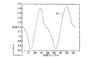
同式中、Tfはフレーム周期であり、Nはフレームごとのライン数である。蛍光管の実際の発光は、図3の曲線20に示すもっと複雑な時間変動を有する。同図は、x軸が時間サンプルを表わし、y軸が照度を表わすグラフである。蛍光管内の蛍光体とフィラメントの特性が原因で、この関数はゆっくりと減衰する。従って、所望とあらば、上記の式(1)により与えられるもっと複雑なフリッカ関数を生成し、曲線にもっと適合させることもできる。
【0026】
本発明の一実施形態によれば、行単位ベースのフリッカ関数でもって画像を表わす画像データを除算することにより画像から偽画像が取り除かれる。画像が二次元データアレイI[i,j]により表される場合、偽画像を除去する処理は下記の如く表わされる。
【0027】
I’[i,j]=I[i,j]/f(j) (2)
【0028】
本発明の一実施形態によれば、フリッカ関数は照明光源のフリッカ周波数とフリッカ振幅とフリッカ位相を算出することにより割り出される。フリッカ周波数とフリッカ振幅とフリッカ位相は、本発明の一実施形態によれば、デジタル画像の各行沿いに画素を寄せ集めて列ベクトルを生成し、フレーム周期と画像フレームごとの交流線繰り返し周波数との積からフリッカ周波数を算出し、補正列ベクトル内のフリッカエネルギを最小化してフリッカの振幅及び位相を割り出すことで算出される。
【0029】
より詳しくは、列ベクトルを作成するため、画像データアレイの全ての列は併せ加算されて列平均を生成する。この処理が、二次元画像データアレイを一次元ベクトルに折りたたむ。この処理は、下式により表わされる。
【0030】
【数1】

【0031】
この式において、Mは画像データの列数である。
【0032】
フリッカの振幅及び位相を算出するため、補正列ベクトル内のフリッカエネルギを最小化するよう、初回の推定が先ずフリッカの振幅及び位相についてなされる。次に、割り出されたフリッカ周波数と推定されたフリッカの振幅及び位相から算出されたフリッカ関数により生成列ベクトルを除算することで、補正列ベクトルが計算される。そこで補正列ベクトル内でフリッカエネルギが計算され、フリッカエネルギがそれ以上低減できるかどうかの判断がなされる。この判断が否定された場合は、推定されたフリッカの振幅及び位相がフリッカ関数の割り出しに用いられる。判断が肯定された場合は、フリッカの振幅及び位相の改善推定がなされ、フリッカエネルギがそれ以上低減できなくなるまで、この手順が繰り返される。
【0033】
補正列ベクトルのフリッカエネルギは、C[j]/f(j)の正弦値及び余弦値を計算することにより算出される。エネルギは、画像データの平均値により正規化した2つの項の二乗の平方根である。
【0034】
【数2】
式(4),(5)中、A(j)は、画像フレーム端での不連続部分がエネルギ値に寄与するのを防止するのに用いるアポディゼーション関数である。この種の関数例には、ハニング関数やハミング関数が含まれる。
【0036】
フリッカエネルギは、下記で表わされる。
【0037】
Ef=√(XS+XC)/<C> (6)
【0038】
式(6)では、平均画像データは列平均から割り出してある。
【0039】
振幅と位相の関数としてのフリッカエネルギの変動により規定される面が図4にプロットしてあり、図ではx軸が振幅を表わしy軸が位相を表わす。図4に示したように、この関数は良好に規定されたユニークな最小値を備えた滑らかなものである。
【0040】
一旦フリッカエネルギが最小化されると、フリッカ周波数の計算値と最小化から得られたフリッカの位相及び振幅の計算値を用いて割り出したフリッカ関数により画像データを除算することで、全画像から偽画像を取り除くことができる。
【0041】
図5,6は、本発明の一実施形態になる方法の効果を示す画像である。図5の画像は、CMOS画像センサすなわち原画像の単色平面からの生データで構成してある。図6の画像は、本発明の一実施形態になるフリッカ補正、すなわちフリッカ補正画像を適用した結果である。図5,6から明らかなように、図5の画像に存在する水平線が図6の画像からは除去されている。
【0042】
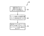
図7は、本発明の一実施形態によるシーンの画像から偽画像を取り除く方法を大略例示するフローチャートである。図7に示すように、本方法はステップ30でのシーンを照らす光源の発光をモデル化するフリッカ関数の割り出しを含むものであり、その後にステップ40でのフリッカ関数を用いてシーンの画像を表わす画像データの処理を含む。
【0043】
図8Aは、本発明の別の実施形態により図7のフリッカ関数を割り出すステップをより詳細に例示するフローチャートである。特に、前述した如く、撮像対象シーンを照明する光源のフリッカ関数を割り出すため、光源のフリッカ周波数とフリッカ振幅とフリッカ位相が割り出される。これは、ステップ50に示したように先ず画像アレイの各行沿いに画像アレイの画素を寄せ集めて列ベクトルを生成することにより、図8Aに開示した如く達成される。フリッカ周波数は、ステップ60に示したように、フレーム周期と画像フレームごとの交流線繰り返し周波数との積から割り出される。フリッカ位相とフリッカ振幅は、ステップ70で示すように補正列ベクトルのフリッカエネルギを最小化することにより割り出される。
【0044】
図8Aに示されるフリッカ位相とフリッカ振幅を割り出すステップを、図8Bでさらに詳細に説明する。具体的には、フリッカの振幅及び位相の初期推定はステップ72に示した如くなされる。それ故に、補正列ベクトルは図8Aのステップ50で生成された列ベクトルをステップ74の推定フリッカ関数で除算することで計算される。この推定フリッカ関数は、図8Aのステップ60で割り出したフリッカ周波数と図8Bのステップ72で推定したフリッカ振幅とフリッカ位相を用いて計算される。補正列ベクトルのフリッカエネルギは次にステップ76において計算され、ステップ78においてフリッカエネルギがさらに低減できるかどうかの判断がなされる。この判断が否定された場合は、ステップ72においてなされたフリッカ振幅とフリッカ位相の初期推定を用いてフリッカ関数が割り出される。判断が肯定された場合は、ステップ80においてフリッカ振幅とフリッカ位相の改善推定がなされ、ステップ74においてさらなる補正列ベクトルが計算され、ステップ76において新たなフリッカエネルギが計算される。この手順は、フリッカエネルギがこれ以上低減できなくなるまで、すなわちステップ78における判断がなされなくなるまで繰り返される。
【0045】
図9は、本発明の一実施形態によりシーンの画像から偽画像を取り除く装置を図示するものである。この装置は、参照符合100により概ね指し示したディジタルカメラなどの撮像装置を備える。撮像装置は、シーンから受光し、CMOS画像センサなどの画像検出ユニット104に光を合焦する図9のレンズにより表わされる光学システム102を含む。画像検出ユニットは、その上の光パターンを画像検出ユニット内に含まれるAD変換器によりディジタル化される電圧サンプルアレイへ変換する。
【0046】
フリッカ関数割り出し器106は、前述したように、光源のフリッカ周波数とフリッカ振幅とフリッカ位相を割り出すことでディジタル画像データから光源のフリッカ関数を割り出し、画像データプロセッサ108はフリッカ関数を用いて画像データを処理し、シーンの生成画像から偽画像を取り除く。
【0047】
ここに説明した内容は本発明の例示実施形態を構成するものであるが、本発明はその範囲を逸脱することなく様々に変形可能であることは認識されたい。従って、本発明が特許請求の範囲により必要とされる範囲内にだけ限定さるべきことは理解されたい。
【0048】
本発明の態様を以下に例示する。
【0049】
1.画像データにより表わされる、光源により照らされたシーンの画像から偽画像を除去する方法であって、フリッカ関数を割り出すステップと、前記フリッカ関数を用いて前記画像データを処理し、前記画像から偽画像を除去するステップを含む方法。
【0050】
2.上記1記載の方法であって、前記画像データは複数行の画像データからなる画像データアレイからなり、前記処理ステップが行単位ベースで前記画像データを前記フリッカ関数により除算するステップを含む方法。
【0051】
3.上記2記載の方法であって、前記フリッカ関数は、前記光源のフリッカ周波数とフリッカ振幅とフリッカ位相の関数である方法。
【0052】
4.上記3記載の方法であって、前記フリッカ関数の割り出しステップが、フレーム周期と画像フレームごとの交流線の繰り返し周波数との積からフリッカ周波数を割り出すことを含む方法。
【0053】
5.上記4記載の方法であって、前記フリッカ関数の割り出しステップはさらに、前記画像データアレイの各行沿いに前記画像データアレイの画素を寄せ集めて列ベクトルを生成するステップを含み、さらに前記補正列ベクトルのフリッカエネルギを最小化することで前記フリッカ位相と前記フリッカ振幅を割り出すステップを含む方法。
【0054】
6.上記5記載の方法であって、補正列ベクトルのフリッカエネルギの前記最小化ステップが、フリッカの振幅及び位相の推定ステップと、割り出されたフリッカ周波数と推定されたフリッカの振幅及び位相とを用いて計算したフリッカ関数により生成列ベクトルを除算することで補正列ベクトルを計算するステップと、補正列ベクトルのフリッカエネルギを計算するステップと、フリッカエネルギがさらに低減できるかどうか判定するステップと、フリッカエネルギがさらに低減できない場合は、推定されたフリッカの振幅及び位相を用いてフリッカ関数を割り出し、フリッカエネルギがさらに低減できる場合は、フリッカエネルギがこれ以上低減できなくなるまで、フリッカの振幅及び位相を推定し、補正列ベクトルを計算し、フリッカエネルギを計算するステップを繰り返すステップを含む方法。
【0055】
7.前記光源は、周期的に変動する光源からなる上記2記載の方法。
【0056】
8.前記周期的に変動する光源は、蛍光源からなる上記7記載の方法。
【0057】
9.前記画像データアレイの行の行番号で表わされる前記フリッカ関数が、
f(j)=1+αsin2(jωTf/N+Φ)
であり、αがフリッカ振幅、ωがフリッカ周波数、Φがフリッカ位相、Tfがフレーム周期、Nが画像フレームごとの行数を表わす上記8記載の方法。
【0058】
10.前記画像データは回転シャッタを用いてCMOS画像センサから収集され、露光制御をもたらす上記1記載の方法。
【0059】
11.複数行の画像データからなる画像データアレイにより表わされる、周期的に変動する光源により照明されたシーンの画像から偽画像を除去する方法であって、周期的に変動する光源の光照射をモデル化したフリッカ関数を割り出すステップと、前記フリッカ関数を用いて前記画像データを処理し、前記画像から偽画像を除去するステップを含む方法。
【0060】
12.上記11記載の方法であって、前記フリッカ関数は、周期的に変動する光源のフリッカ振幅とフリッカ周波数とフリッカ位相の関数である方法。
【0061】
13.上記12記載の方法であって、フリッカ関数を割り出す前記ステップが、画像データアレイの各行沿いに画素を寄せ集めて列ベクトルを生成し、フレーム周期と画像フレームごとの交流線の繰り返し周波数との積からフリッカ周波数を割り出すステップと、補正列ベクトルのフリッカエネルギを最小化することによりフリッカの振幅及び位相を割り出すステップとを含む方法。
【0062】
14.上記13記載の方法であって、補正列ベクトルのフリッカエネルギを最小化する前記ステップが、フリッカの振幅及び位相の推定ステップと、割り出されたフリッカ周波数と推定されたフリッカの振幅及び位相とを用いて計算したフリッカ関数により生成列ベクトルを除算することで補正列ベクトルを計算するステップと、補正列ベクトルのフリッカエネルギを計算するステップと、フリッカエネルギがさらに低減できるかどうか判定するステップと、フリッカエネルギがさらに低減できない場合は、推定されたフリッカの振幅及び位相を用いてフリッカ関数を割り出し、フリッカエネルギがさらに低減できる場合は、フリッカエネルギがこれ以上低減できなくなるまで、フリッカの振幅及び位相を推定し、補正列ベクトルを計算し、フリッカエネルギを計算するステップを繰り返すステップを含む方法。
【0063】
15.上記11記載の方法であって、前記周期的に変動する光源は蛍光源からなり、前記画像データアレイの行の行番号で表わされる前記フリッカ関数が、
f(j)=1+αsin2(jωTf/N+Φ)
であり、αがフリッカ振幅、ωがフリッカ周波数、Φがフリッカ位相、Tfがフレーム周期、Nが画像フレームごとの行数を表わす方法。
【0064】
16.上記11記載の方法であって、前記画像データは回転シャッタを用いてCMOS画像センサから収集され、画像制御をもたらす方法。
【0065】
17.光源によって照らされたシーンの画像から偽画像を除去する装置であって、前記シーンを表わす画像データを供給するユニットと、フリッカ関数を割り出すフリッカ関数割り出し器と、前記フリッカ関数を用いて前記画像データを処理し、前記画像から前記偽画像を除去する画像データプロセッサを備える装置。
【0066】
18.上記17記載の装置であって、前記画像データが複数行の画像データからなる画像データアレイを含み、前記画像データプロセッサが行単位ベースで前記画像データを前記フリッカ関数により除算することで前記画像データを処理する装置。
【0067】
19.上記18記載の装置であって、前記フリッカ関数は、前記光源のフリッカ周波数とフリッカ振幅とフリッカ位相の関数であり、前記フリッカ関数割り出し器が前記フリッカ周波数と前記フリッカ振幅と前記フリッカ位相を割り出す手段を含む装置。
【0068】
20. 前記光源は、蛍光源からなる上記17記載の装置。
【0069】
21.ディジタル撮像方法であって、ディジタル画像を分析してフリッカ関数を割り出すステップと、前記フリッカ関数を用いて前記ディジタル画像を処理し、該ディジタル画像から偽画像を低減するステップとを含み、前記割り出しステップが前以て定めたフリッカモデルに関連するパラメータ値の割り出しを含む方法。
【0070】
22.前記処理ステップが、前記ディジタル画像を前記フリッカ関数により除算するステップを含む上記21記載のディジタル撮像方法。
【0071】
23.前記割り出しステップが、フリッカ周波数とフリッカ振幅とフリッカ位相の算出を含む上記21記載のディジタル撮像方法。
【0072】
24.上記23記載のディジタル撮像方法であって、フリッカ周波数とフリッカ振幅とフリッカ位相の前記割り出しステップが、画像データアレイの各行沿いに画素を寄せ集めて列ベクトルを生成し、フレーム周期と画像フレームごとの交流線の繰り返し周波数との積からフリッカ周波数を割り出すステップと、補正列ベクトルのフリッカエネルギを最小化することによりフリッカの振幅及び位相を割り出すステップとを含む方法。
【0073】
25.上記24記載のディジタル撮像方法であって、前記補正列ベクトルのフリッカエネルギを最小化するステップが、フリッカの振幅及び位相を推定するステップと、割り出されたフリッカ周波数と推定されたフリッカの振幅及び位相を用いて計算したフリッカ関数により生成列ベクトルを除算することにより補正列ベクトルを計算するステップと、補正列ベクトルのフリッカエネルギを算出するステップと、フリッカエネルギがさらに低減できるかどうか判定するステップと、フリッカエネルギがさらに低減できない場合は、推定されたフリッカの振幅及び位相を用いてフリッカ関数を割り出し、フリッカエネルギがさらに低減できる場合は、フリッカエネルギがこれ以上低減できなくなるまで、フリッカの振幅及び位相を推定し、補正列ベクトルを計算し、フリッカエネルギを計算するステップを繰り返すステップを含む方法。
【0074】
26.ディジタル画像処理システムであって、ディジタル画像のフリッカ関数を割り出す手段と、前記フリッカ関数を用いて前記ディジタル画像内の偽画像を低減する該ディジタル画像の処理手段とを備えるシステム。
【図面の簡単な説明】
【図1】本発明の明瞭な理解を助ける回転シャッタの動作を概略説明する図である。
【図2】回転シャッタを用いてCMOS画像センサの出力上のフリッカの影響を例示する概略画像である。
【図3】蛍光管の発光特性を例示するグラフである。
【図4】本発明の一実施形態になるフリッカ補正を例示するグラフである。
【図5】本発明の一実施形態の方法と装置の効果を表わす図であり、回転シャッタを用いたCMOS画像センサの単色平面からの生データの画像である。
【図6】本発明の一実施形態の方法と装置の効果を表わす図であり、本発明の一実施形態によりフリッカ補正を適用した結果得られる画像である。
【図7】本発明の一実施形態による偽画像を画像から除去する方法のステップを示すフローチャートである。
【図8A】本発明の他の実施形態による図7のフリッカ関数の割り出しステップを詳細に示すフローチャートである。
【図8B】本発明の他の実施形態による図8Aのフリッカの位相及び振幅の割り出しステップを詳細に示すフローチャートである。
【図9】本発明の他の実施形態による偽画像を画像から除去する装置を概略示す図である。
【符号の説明】
10 露光期間
14 概略画像
16 水平バー
100 撮像装置
102 光学システム
104 画像検出ユニット
106 フリッカ関数割り出し器
108 画像データプロセッサ[0001]
BACKGROUND OF THE INVENTION
The present invention relates generally to the field of image processing, and more specifically to a method and apparatus for removing false images produced by a periodically varying light source from an image.
[0002]
[Prior art]
In a CMOS (complementary metal oxide semiconductor) active pixel image sensor, a rotary shutter is generally used for exposure control. The rotary shutter operates by sequentially resetting the sensor rows of the image sensor column and sequentially reading the values of the rows later. The exposure period is equal to the reset and read time interval, and the frame period is the time required to read the value of each row in the array.
[0003]
FIG. 1 is a diagram schematically illustrating the operation of a rotary shutter so that the present invention can be clearly understood. Consider an image data array having 100 rows (FIG. 1 shows only 9 rows for convenience). Assume that the time required for reading a single row, that is, the row period is T, and the exposure period indicated by the
[0004]
One characteristic of the rotary shutter is that the exposure for each row occurs over different time periods, as shown in FIG. Therefore, when the scene illumination varies with time, the brightness of the captured image varies from row to row. If the variation period in the illumination level of the scene is longer than the accumulation period of the rotary shutter and shorter than the frame period, the variation results in the appearance of image artifacts in the form of horizontal bands in the image. The number of bands in the image is equal to the flicker period divided by the frame period.
[0005]
These time variations in the illuminance level of the light source are known as “flicker” and the horizontal band of the image is called a fake image or “flicker pattern”. For example, fluorescent lamps have very strong flicker. The lamp phosphor is excited at each peak of the power line frequency and decays between the peaks. The generated light pulse has a flicker frequency twice that of the AC power line. Incandescent bulbs do not exhibit flicker because the amount of heat in the filament is large enough to prevent the filament from cooling significantly between AC peaks.
[0006]
The effect of flicker on the output of a CMOS image sensor is illustrated in the
[0007]
The number of horizontal bars in the image as shown in FIG. 2 is equal to the ratio of the frame period to the flicker period. The amplitude of the horizontal bar depends on the characteristics of the specific light source and the integration period of the rotary shutter of the CMOS image sensor.
[0008]
Several methods have been devised to remove flicker from frame to frame. For example, U.S. Pat. No. 5,793,886 discloses a method in which histograms of different image frames are compared, thereby removing the variation in average illumination as a function of time. However, the method described here can only be used for a single image frame and is not applicable to situations where flicker is manifested as a series of horizontal bands in the generated image.
[0009]
Another known method of removing flicker from frame to frame is to monitor the brightness of the light source during the frame exposure period. For example, in the method described in US Pat. No. 6,208,433, a separate sensor is used for light source fluctuation monitoring, and the output of this sensor is used for image correction. In US Pat. No. 5,960,153, linear image sensors are used for both imaging and measuring light source fluctuations. The light source variation is used for exposure time control, so that flicker does not appear in the final image.
[0010]
In another known method, flicker is prevented by limiting the exposure period to an integral multiple of the flicker cycle. Under this type of situation, each row accumulates light at an integral multiple of the total period of light source variation. As a result, the integrated light level is the same for each row, and no band appears in the image. The disadvantage of this method is that the exposure period cannot be shorter than the flicker period. If the light source is very bright and the exposure period cannot be reduced, the generated image will be overexposed. This type of problem can occur when the scene is illuminated with a bright fluorescent source or when the camera is pointed directly at the fluorescent source.
[0011]
[Problems to be solved by the invention]
In general, known methods for removing frame-by-frame flicker from an image require several consecutive image frames for processing, need to monitor flicker independently, or require additional input. Therefore, the known methods for flicker removal are not completely satisfactory. What is needed is to eliminate flicker generated by a periodically fluctuating light source acting on a single image, no flicker period and frame period values are required, and flicker is independent Methods and devices that do not need to be monitored. What is also needed is a method and apparatus that can be used to capture images with very low flicker even under very bright fluorescent illumination.
[0012]
[Means for Solving the Problems]
The present invention provides a method and apparatus for removing false images from an image generated by a periodically varying light source such as a fluorescent source. The method according to the present invention removes false images from an image represented by image data. In this method, a flicker function is determined, and image data is processed using the flicker function to remove a false image.
[0013]
According to the present invention, it has been found that by processing an image using a flicker function that models light irradiation of a light source that illuminates an imaging scene, a false image can be removed or greatly reduced from the image. The present invention is particularly suitable for removing false images from an image represented by image data collected from a CMOS image sensor using a rotating shutter.
[0014]
According to an embodiment of the present invention, the image data representing an image is composed of an image data array composed of a plurality of rows of image data, and the image data processing step divides the image data by a flicker function on a row-by-row basis. Consists of.
[0015]
The determination of the flicker function of the image data includes the determination of parameter values related to the flicker model prepared in advance. In particular, the flicker frequency, flicker amplitude, and flicker phase of the light source are determined to determine the flicker function. In one embodiment of the present invention, the flicker frequency, flicker amplitude, and flicker phase are obtained by gathering pixels along each row of the image data array to generate a column vector, which is the product of the frame period and the AC line repetition frequency for each image frame. From this, the flicker frequency is determined, the flicker energy in the correction sequence vector is minimized, and the flicker amplitude and phase are determined.
[0016]
More specifically, according to a further embodiment of the present invention, an initial estimation of flicker amplitude and phase is performed, and a generated column vector is calculated by a flicker function calculated from the determined flicker frequency and the estimated flicker amplitude and phase. Dividing to calculate the correction column vector and calculating the flicker energy in the correction column vector, the flicker amplitude and phase are determined. Therefore, it is determined whether or not the flicker energy can be further reduced. If the determination is negative, the estimated flicker amplitude and phase are used to determine the flicker function. If the determination is affirmative, the flicker amplitude and phase estimates are amended, a further corrected column vector is calculated, and the corrected column vector is used to calculate the flicker energy. This procedure is repeated until the flicker energy can no longer be reduced.
[0017]
Once the flicker energy is minimized, the flicker is removed from the image data by dividing the image data by the determined flicker function.
[0018]
The method of the present invention has the advantage of eliminating flicker caused by any periodically fluctuating light source such as a fluorescent source. Any exposure period can be used in the method of the present invention, so that the method can be used to capture images with significantly reduced flicker even under bright fluorescent sources. The present invention eliminates false images that act on a single image from the image, does not require any additional input other than flicker and frame period values, and does not require flicker to be monitored independently. It is to provide. Furthermore, the present invention provides embodiments with other features and advantages in addition to or in lieu of those described above. Many of these features and advantages will become apparent from the following drawings and detailed description of exemplary embodiments of the invention.
[0019]
DETAILED DESCRIPTION OF THE INVENTION
In a CMOS image sensor operating in the rotary shutter mode, the exposure period of the image data array varies from row to row within the array shown in FIG. 1 (however, in a particular row, all pixels are exposed over the same period. To do). When the intensity of the light source that illuminates the imaging scene varies with time, the intensity may vary for each row in the image data. If the row period is fixed and the light source intensity varies periodically with time, the intensity variation appears as a false image in the form of a periodic horizontal bar in the image generated from the image data.
[0020]
If the integration period is equal to an integer multiple of the flicker period, the horizontal bar amplitude will be zero. However, it is generally not possible to determine the bar amplitude in advance because the characteristics of the light source are not known. In addition, the vertical arrangement of horizontal bar patterns for an image depends on the phase of light flicker at the beginning of the exposure period. However, like amplitude, phase cannot also be determined in advance.
[0021]
The blinking of the fluorescence is caused by the power supply of light. The fluorescent tube includes a filament that emits electrons into the mercury vapor atomic cloud. Vapor atoms are excited and emit ultraviolet (UV) light. When the ultraviolet light hits the tube vessel of the fluorescent tube, the ultraviolet light excites the phosphor on the inner surface of the tube. The phosphor then fluoresces and emits white light.
[0022]
Electron emission is maximized at the peak of the drive voltage of the power supply. Since there are two peaks per period, the flicker frequency is twice the drive voltage frequency. Therefore, the fluorescent tube fed by the 60 Hz electrical system blinks at 120 Hz.
[0023]
Function (1 + αsin 2 (Ωt + Φ)) can be used to model the illumination of the fluorescent tube. In the equation, α is the flicker amplitude, ω is the flicker frequency, and Φ is the flicker phase. This flicker function can also be expressed as the following equation with the row number of the row of the image array.
[0024]
f (j) = 1 + αsin 2 (JωT f / N + Φ) (1)
[0025]
T f Is the frame period, and N is the number of lines per frame. The actual emission of the fluorescent tube has a more complex time variation as shown by
[0026]
According to one embodiment of the present invention, false images are removed from an image by dividing the image data representing the image by a line-based flicker function. When the image is represented by the two-dimensional data array I [i, j], the process of removing the fake image is represented as follows.
[0027]
I ′ [i, j] = I [i, j] / f (j) (2)
[0028]
According to one embodiment of the invention, the flicker function is determined by calculating the flicker frequency, flicker amplitude and flicker phase of the illumination light source. According to an embodiment of the present invention, the flicker frequency, the flicker amplitude, and the flicker phase are generated by collecting pixels along each row of a digital image to generate a column vector, and calculating a frame period and an AC line repetition frequency for each image frame. The flicker frequency is calculated from the product, and the flicker energy in the correction sequence vector is minimized to determine the flicker amplitude and phase.
[0029]
More specifically, to create a column vector, all columns of the image data array are added together to produce a column average. This process folds the two-dimensional image data array into a one-dimensional vector. This process is expressed by the following equation.
[0030]
[Expression 1]
[0031]
In this equation, M is the number of columns of image data.
[0032]
In order to calculate the flicker amplitude and phase, an initial estimation is first made on the flicker amplitude and phase so as to minimize the flicker energy in the correction sequence vector. Next, a corrected column vector is calculated by dividing the generated column vector by the flicker function calculated from the calculated flicker frequency and the estimated flicker amplitude and phase. Therefore, the flicker energy is calculated in the correction column vector, and it is determined whether the flicker energy can be further reduced. If this determination is negative, the estimated flicker amplitude and phase are used to determine the flicker function. If the determination is affirmative, an improvement estimate of the flicker amplitude and phase is made and this procedure is repeated until the flicker energy cannot be reduced any further.
[0033]
The flicker energy of the correction column vector is calculated by calculating the sine value and cosine value of C [j] / f (j). The energy is the square root of the square of the two terms normalized by the average value of the image data.
[0034]
[Expression 2]
In equations (4) and (5), A (j) is an apodization function used to prevent the discontinuity at the image frame end from contributing to the energy value. Examples of this type of function include a Hanning function and a Hamming function.
[0036]
The flicker energy is expressed below.
[0037]
E f = √ (X S + X C ) / <C> (6)
[0038]
In equation (6), the average image data is determined from the column average.
[0039]
The plane defined by the flicker energy variation as a function of amplitude and phase is plotted in FIG. 4, where the x-axis represents amplitude and the y-axis represents phase. As shown in FIG. 4, this function is smooth with a well-defined unique minimum.
[0040]
Once the flicker energy is minimized, the image data is divided by the flicker function calculated using the calculated flicker frequency and the calculated flicker phase and amplitude from the minimization. The image can be removed.
[0041]
5 and 6 are images showing the effect of the method according to one embodiment of the present invention. The image of FIG. 5 is composed of a CMOS image sensor, that is, raw data from a monochromatic plane of the original image. The image in FIG. 6 is a result of applying the flicker correction, that is, the flicker correction image according to the embodiment of the present invention. As is apparent from FIGS. 5 and 6, the horizontal line existing in the image of FIG. 5 is removed from the image of FIG. 6.
[0042]
FIG. 7 is a flowchart schematically illustrating a method of removing a fake image from a scene image according to an embodiment of the present invention. As shown in FIG. 7, the method includes the determination of a flicker function that models the light emission of the light source that illuminates the scene at
[0043]
FIG. 8A is a flowchart illustrating in more detail the steps of determining the flicker function of FIG. 7 according to another embodiment of the invention. In particular, as described above, in order to determine the flicker function of the light source that illuminates the scene to be imaged, the flicker frequency, flicker amplitude, and flicker phase of the light source are determined. This is accomplished as disclosed in FIG. 8A by first gathering the pixels of the image array along each row of the image array as shown in
[0044]
The step of determining the flicker phase and flicker amplitude shown in FIG. 8A will be described in more detail with reference to FIG. 8B. Specifically, initial estimation of flicker amplitude and phase is performed as shown in
[0045]
FIG. 9 illustrates an apparatus for removing a fake image from a scene image according to an embodiment of the present invention. This apparatus comprises an imaging device, such as a digital camera, generally indicated by
[0046]
As described above, the
[0047]
Although the contents described herein constitute exemplary embodiments of the present invention, it should be recognized that the present invention can be variously modified without departing from the scope thereof. Accordingly, it is to be understood that the invention is limited only to the extent required by the appended claims.
[0048]
Embodiments of the present invention are exemplified below.
[0049]
1. A method for removing a fake image from an image of a scene illuminated by a light source represented by image data, comprising: calculating a flicker function; processing the image data using the flicker function; A method comprising the step of removing.
[0050]
2. 2. The method according to claim 1, wherein the image data includes an image data array including a plurality of rows of image data, and the processing step includes a step of dividing the image data by the flicker function on a row-by-row basis.
[0051]
3. 3. The method according to 2 above, wherein the flicker function is a function of a flicker frequency, a flicker amplitude, and a flicker phase of the light source.
[0052]
4). 4. The method of claim 3, wherein the step of determining the flicker function includes determining a flicker frequency from a product of a frame period and a repetition frequency of an AC line for each image frame.
[0053]
5. 5. The method according to claim 4, wherein the step of determining the flicker function further includes a step of generating a column vector by collecting pixels of the image data array along each row of the image data array, and further comprising the correction column vector. Determining the flicker phase and the flicker amplitude by minimizing the flicker energy.
[0054]
6). 6. The method of claim 5, wherein the step of minimizing the flicker energy of the correction sequence vector uses a flicker amplitude and phase estimation step, the determined flicker frequency and the estimated flicker amplitude and phase. Calculating the correction column vector by dividing the generated column vector by the calculated flicker function, calculating the flicker energy of the correction column vector, determining whether the flicker energy can be further reduced, and flicker energy. If the flicker energy cannot be further reduced, the flicker energy and the phase are estimated until the flicker energy cannot be further reduced. Calculate the correction column vector and flicker energy Method comprising the step of repeating the step of calculating the formic.
[0055]
7). 3. The method according to 2 above, wherein the light source comprises a periodically varying light source.
[0056]
8). 8. The method of claim 7, wherein the periodically varying light source comprises a fluorescent source.
[0057]
9. The flicker function represented by the row number of the row of the image data array is:
f (j) = 1 + αsin 2 (JωT f / N + Φ)
Where α is the flicker amplitude, ω is the flicker frequency, Φ is the flicker phase, T f 9. The method of claim 8, wherein is the frame period and N is the number of rows per image frame.
[0058]
10. The method of claim 1, wherein the image data is collected from a CMOS image sensor using a rotating shutter to provide exposure control.
[0059]
11. A method for removing fake images from a scene image illuminated by a periodically varying light source, represented by an image data array consisting of multiple rows of image data, modeling light illumination of a periodically varying light source Determining a flicker function, and processing the image data using the flicker function to remove a false image from the image.
[0060]
12 12. The method according to 11 above, wherein the flicker function is a function of a flicker amplitude, a flicker frequency, and a flicker phase of a light source that varies periodically.
[0061]
13. 13. The method according to claim 12, wherein the step of calculating a flicker function includes a pixel vector gathered along each row of the image data array to generate a column vector, and a product of a frame period and an AC line repetition frequency for each image frame. And determining the flicker amplitude and phase by minimizing the flicker energy of the correction sequence vector.
[0062]
14 14. The method of claim 13, wherein the step of minimizing the flicker energy of the correction sequence vector comprises the step of estimating the flicker amplitude and phase, the determined flicker frequency and the estimated flicker amplitude and phase. Calculating a correction column vector by dividing the generated column vector by the calculated flicker function, calculating a flicker energy of the correction column vector, determining whether the flicker energy can be further reduced, and a flicker. If the energy cannot be further reduced, use the estimated flicker amplitude and phase to determine the flicker function, and if the flicker energy can be further reduced, estimate the flicker amplitude and phase until the flicker energy can no longer be reduced. Calculate the correction column vector and Method comprising the step of repeating the step of calculating the energy.
[0063]
15. 12. The method according to 11 above, wherein the periodically varying light source is a fluorescent source, and the flicker function represented by a row number of a row of the image data array is:
f (j) = 1 + αsin 2 (JωT f / N + Φ)
Where α is the flicker amplitude, ω is the flicker frequency, Φ is the flicker phase, T f Represents the frame period and N represents the number of rows per image frame.
[0064]
16. 12. The method of claim 11, wherein the image data is collected from a CMOS image sensor using a rotary shutter to provide image control.
[0065]
17. An apparatus for removing a false image from an image of a scene illuminated by a light source, the unit supplying image data representing the scene, a flicker function indexer for calculating a flicker function, and the image data using the flicker function And an image data processor for removing the fake image from the image.
[0066]
18. 18. The apparatus according to 17, wherein the image data includes an image data array including image data of a plurality of rows, and the image data processor divides the image data by the flicker function on a row unit basis. Processing equipment.
[0067]
19. 19. The apparatus according to claim 18, wherein the flicker function is a function of a flicker frequency, a flicker amplitude, and a flicker phase of the light source, and the flicker function indexer determines the flicker frequency, the flicker amplitude, and the flicker phase. Including the device.
[0068]
20. 18. The apparatus according to 17 above, wherein the light source is a fluorescent source.
[0069]
21. A digital imaging method comprising: analyzing a digital image to determine a flicker function; and processing the digital image using the flicker function to reduce false images from the digital image, the determining step A method involving the determination of parameter values associated with a predefined flicker model.
[0070]
22. 22. The digital imaging method according to claim 21, wherein the processing step includes a step of dividing the digital image by the flicker function.
[0071]
23. 22. The digital imaging method according to 21 above, wherein the determining step includes calculation of a flicker frequency, a flicker amplitude, and a flicker phase.
[0072]
24. 24. The digital imaging method according to 23, wherein the step of determining the flicker frequency, the flicker amplitude, and the flicker phase generates a column vector by collecting pixels along each row of the image data array, A method comprising: determining a flicker frequency from a product of the AC line repetition frequency and determining the flicker amplitude and phase by minimizing the flicker energy of the correction sequence vector.
[0073]
25. 25. The digital imaging method according to 24, wherein the step of minimizing the flicker energy of the correction sequence vector includes the step of estimating the flicker amplitude and phase, the determined flicker frequency and the estimated flicker amplitude and Calculating a correction column vector by dividing the generated column vector by a flicker function calculated using the phase; calculating a flicker energy of the correction column vector; and determining whether the flicker energy can be further reduced. If the flicker energy cannot be further reduced, the flicker function is calculated by using the estimated flicker amplitude and phase. If the flicker energy can be further reduced, the flicker amplitude and phase until the flicker energy cannot be further reduced. And the correction column vector The method comprising repeating the step of calculating the Le, calculates the flicker energy.
[0074]
26. A digital image processing system, comprising: means for determining a flicker function of a digital image; and processing means for the digital image that reduces false images in the digital image using the flicker function.
[Brief description of the drawings]
FIG. 1 is a diagram schematically illustrating the operation of a rotary shutter that helps a clear understanding of the present invention.
FIG. 2 is a schematic image illustrating the effect of flicker on the output of a CMOS image sensor using a rotating shutter.
FIG. 3 is a graph illustrating the emission characteristics of a fluorescent tube.
FIG. 4 is a graph illustrating flicker correction according to an embodiment of the present invention.
FIG. 5 is a diagram representing the effect of the method and apparatus of an embodiment of the present invention, which is an image of raw data from a monochromatic plane of a CMOS image sensor using a rotating shutter.
FIG. 6 is a diagram representing the effect of the method and apparatus of an embodiment of the present invention, and is an image obtained as a result of applying flicker correction according to an embodiment of the present invention.
FIG. 7 is a flowchart illustrating the steps of a method for removing a false image from an image according to an embodiment of the present invention.
8A is a flowchart illustrating in detail a flicker function determination step of FIG. 7 according to another embodiment of the present invention.
8B is a flowchart detailing the flicker phase and amplitude determination steps of FIG. 8A according to another embodiment of the present invention.
FIG. 9 schematically illustrates an apparatus for removing a false image from an image according to another embodiment of the present invention.
[Explanation of symbols]
10 Exposure period
14 Outline image
16 Horizontal bar
100 Imaging device
102 Optical system
104 Image detection unit
106 Flicker function indexer
108 Image data processor
Claims (7)
前記画像データは、複数行の画像データからなる画像データアレイからなり、
フリッカ関数を割り出すステップと、
行単位ベースで前記画像データを前記フリッカ関数により除算し、前記画像から偽画像を除去または減少する処理ステップ、を含み、
前記フリッカ関数は、前記光源のフリッカ周波数とフリッカ振幅とフリッカ位相の関数であり、
前記フリッカ関数の割り出しステップが、フレーム周期と画像フレームごとの交流線の繰り返し周波数との積からフリッカ周波数を割り出すことを含む
ことを特徴とする方法。A method for removing or reducing fake images from an image of a scene illuminated by a light source represented by image data, comprising:
The image data comprises an image data array consisting of a plurality of rows of image data,
Determining the flicker function;
Processing to divide the image data on a line-by-line basis by the flicker function to remove or reduce false images from the image ;
The flicker function is a function of the flicker frequency, flicker amplitude and flicker phase of the light source,
The step of determining the flicker function includes determining the flicker frequency from the product of the frame period and the AC line repetition frequency for each image frame.
A method characterized by that .
前記フリッカ関数の割り出しステップはさらに、前記画像データアレイの各行沿いに前記画像データアレイの画素を寄せ集めて列ベクトルを生成するステップを含み、
さらに前記補正列ベクトルのフリッカエネルギを最小化することで前記フリッカ位相と前記フリッカ振幅を割り出すステップを含む方法。The method of claim 1 , comprising:
The step of determining the flicker function further includes gathering pixels of the image data array along each row of the image data array to generate a column vector;
The method further includes determining the flicker phase and the flicker amplitude by minimizing the flicker energy of the correction column vector.
補正列ベクトルのフリッカエネルギの前記最小化ステップが、フリッカの振幅及び位相の推定ステップと、割り出されたフリッカ周波数と推定されたフリッカの振幅及び位相とを用いて計算したフリッカ関数により生成列ベクトルを除算することで補正列ベクトルを計算するステップと、補正列ベクトルのフリッカエネルギを計算するステップと、フリッカエネルギがさらに低減できるかどうか判定するステップと、フリッカエネルギがさらに低減できない場合は、推定されたフリッカの振幅及び位相を用いてフリッカ関数を割り出し、フリッカエネルギがさらに低減できる場合は、フリッカエネルギがこれ以上低減できなくなるまで、フリッカの振幅及び位相を推定し、補正列ベクトルを計算し、フリッカエネルギを計算するステップを繰り返すステップを含む方法。The method of claim 2 , comprising:
The step of minimizing the flicker energy of the correction column vector is generated by a flicker function calculated using the flicker amplitude and phase estimation step, the calculated flicker frequency and the estimated flicker amplitude and phase. And calculating the correction column vector, dividing the correction column vector, calculating the flicker energy of the correction column vector, determining whether the flicker energy can be further reduced, and estimating if the flicker energy cannot be further reduced. If the flicker function is calculated using the flicker amplitude and phase and the flicker energy can be further reduced, the flicker amplitude and phase are estimated until the flicker energy can no longer be reduced, the correction column vector is calculated, and the flicker energy is calculated. Repeat the steps to calculate energy The method comprising the step to return.
f(j)=1+αsin2(jωTf/N+Φ)
であり、αがフリッカ振幅、ωがフリッカ周波数、Φがフリッカ位相、Tfがフレーム周期、Nが画像フレームごとの行数を表わす請求項5記載の方法。The flicker function represented by the row number of the row of the image data array is:
f (j) = 1 + αsin 2 (jωT f / N + Φ)
6. The method of claim 5 wherein α represents the flicker amplitude, ω represents the flicker frequency, Φ represents the flicker phase, T f represents the frame period, and N represents the number of rows per image frame.
Applications Claiming Priority (2)
| Application Number | Priority Date | Filing Date | Title |
|---|---|---|---|
| US09/927,201 | 2001-08-10 | ||
| US09/927,201 US7298401B2 (en) | 2001-08-10 | 2001-08-10 | Method and apparatus for removing flicker from images |
Publications (3)
| Publication Number | Publication Date |
|---|---|
| JP2003110880A JP2003110880A (en) | 2003-04-11 |
| JP2003110880A5 JP2003110880A5 (en) | 2005-10-27 |
| JP4200516B2 true JP4200516B2 (en) | 2008-12-24 |
Family
ID=25454378
Family Applications (1)
| Application Number | Title | Priority Date | Filing Date |
|---|---|---|---|
| JP2002212267A Expired - Lifetime JP4200516B2 (en) | 2001-08-10 | 2002-07-22 | How to remove flicker from an image |
Country Status (4)
| Country | Link |
|---|---|
| US (1) | US7298401B2 (en) |
| EP (1) | EP1289285B1 (en) |
| JP (1) | JP4200516B2 (en) |
| DE (1) | DE60239438D1 (en) |
Families Citing this family (47)
| Publication number | Priority date | Publication date | Assignee | Title |
|---|---|---|---|---|
| FI111417B (en) * | 2001-06-01 | 2003-07-15 | Nokia Corp | Control of flash light in a digital camera |
| US6911966B2 (en) * | 2001-08-24 | 2005-06-28 | Koninklijke Philips Electronics N.V. | Matrix display device |
| KR100460755B1 (en) * | 2002-10-10 | 2004-12-14 | 매그나칩 반도체 유한회사 | Pixel array for image sensor and image sensor having the same and auto removal method for flicker noise of image sensor |
| JP4423889B2 (en) * | 2002-11-18 | 2010-03-03 | ソニー株式会社 | Flicker reduction method, imaging apparatus, and flicker reduction circuit |
| US7768500B2 (en) * | 2003-06-16 | 2010-08-03 | Humanscale Corporation | Ergonomic pointing device |
| JP4259998B2 (en) * | 2003-12-19 | 2009-04-30 | 三洋電機株式会社 | Flicker detection device and imaging device |
| US7557799B2 (en) | 2004-06-17 | 2009-07-07 | Avago Technologies Ecbu Ip (Singapore) Pte. Ltd. | System for determining pointer position, movement, and angle |
| US7920175B2 (en) * | 2005-01-13 | 2011-04-05 | Canon Kabushiki Kaisha | Electronic still camera performing composition of images and image capturing method therefor |
| JP4207926B2 (en) * | 2005-05-13 | 2009-01-14 | ソニー株式会社 | Flicker correction method, flicker correction apparatus, and imaging apparatus |
| JP4335849B2 (en) * | 2005-06-13 | 2009-09-30 | 富士通マイクロエレクトロニクス株式会社 | Imaging device capable of flicker detection |
| JP4453648B2 (en) * | 2005-06-13 | 2010-04-21 | ソニー株式会社 | Image processing apparatus and imaging apparatus |
| JP2007006049A (en) * | 2005-06-23 | 2007-01-11 | Funai Electric Co Ltd | Solid-state imaging device |
| JP4371108B2 (en) * | 2005-12-27 | 2009-11-25 | ソニー株式会社 | Imaging apparatus and method, recording medium, and program |
| US7561190B2 (en) * | 2006-04-19 | 2009-07-14 | Nethra Imaging Inc. | Method and system to reduce flicker artifacts in captured images |
| US8068140B2 (en) * | 2006-08-07 | 2011-11-29 | Avago Technologies General Ip (Singapore) Pte. Ltd. | Still image stabilization suitable for compact camera environments |
| JP2008109370A (en) * | 2006-10-25 | 2008-05-08 | Sanyo Electric Co Ltd | Image correcting device and method, and imaging apparatus |
| JP2009017214A (en) * | 2007-07-04 | 2009-01-22 | Canon Inc | Flicker detection apparatus and flicker detection method |
| US8081235B2 (en) * | 2007-11-12 | 2011-12-20 | Canon Kabushiki Kaisha | Image pickup apparatus and flicker detection method therefor |
| US9055260B2 (en) * | 2007-12-17 | 2015-06-09 | Echostar Technologies L.L.C. | Electronic program guide generation apparatus, systems, and methods |
| US7911505B2 (en) * | 2008-08-20 | 2011-03-22 | Eastman Kodak Company | Detecting illuminant flicker |
| US8451356B2 (en) * | 2008-10-09 | 2013-05-28 | Sony Corporation | System and method for correcting artifacts in sequential imagers caused by transient light disturbances |
| US8441551B2 (en) * | 2008-11-14 | 2013-05-14 | Ati Technologies Ulc | Flicker detection circuit for imaging sensors that employ rolling shutters |
| EP2200277A1 (en) * | 2008-12-22 | 2010-06-23 | Thomson Licensing | Method and device to capture images by emulating a mechanical shutter |
| JP2011091775A (en) | 2009-10-26 | 2011-05-06 | Toshiba Corp | Solid-state image pickup device |
| DE112010004379T5 (en) * | 2009-11-13 | 2012-11-29 | Steven Donald Edelson | Surveillance and camera system and procedures |
| JP5625371B2 (en) * | 2010-01-29 | 2014-11-19 | ソニー株式会社 | Image processing apparatus, signal processing method, and program |
| US8711245B2 (en) * | 2011-03-18 | 2014-04-29 | Digitaloptics Corporation Europe Ltd. | Methods and systems for flicker correction |
| US9088727B2 (en) | 2011-04-06 | 2015-07-21 | Pelco, Inc. | Spatially-varying flicker detection |
| US8928735B2 (en) | 2011-06-14 | 2015-01-06 | Microsoft Corporation | Combined lighting, projection, and image capture without video feedback |
| US9560314B2 (en) | 2011-06-14 | 2017-01-31 | Microsoft Technology Licensing, Llc | Interactive and shared surfaces |
| US8903043B2 (en) | 2011-10-24 | 2014-12-02 | Bruker Axs, Inc. | Method for correcting timing skew in X-ray data read out of an X-ray detector in a rolling shutter mode |
| KR102020941B1 (en) | 2013-02-08 | 2019-09-11 | 삼성전자주식회사 | Motion estimation device and estimation method thereof |
| US9083887B2 (en) * | 2013-04-08 | 2015-07-14 | Samsung Electronics Co., Ltd. | Image capture devices configured to generate compensation gains based on an optimum light model and electronic apparatus having the same |
| US9554048B2 (en) * | 2013-09-26 | 2017-01-24 | Apple Inc. | In-stream rolling shutter compensation |
| EP2950523A1 (en) * | 2014-05-28 | 2015-12-02 | Thomson Licensing | Method of estimating flicker on recorded video by camcorder |
| JP6525715B2 (en) * | 2015-05-08 | 2019-06-05 | キヤノン株式会社 | Image pickup apparatus, detection method of light amount change, and program |
| US9571749B2 (en) * | 2015-05-26 | 2017-02-14 | Novatek Microelectronics Corp. | Flicker detecting method for image capturing device |
| KR102523301B1 (en) * | 2015-12-15 | 2023-04-19 | 삼성전자주식회사 | Image sensor circuit removing flicker and camera device including the same |
| RU2658811C2 (en) * | 2016-12-12 | 2018-06-22 | Общество С Ограниченной Ответственностью "Дисикон" | Method and system of elimination of the effect of the sliding shutter of the camera |
| WO2018211511A1 (en) * | 2017-05-16 | 2018-11-22 | Technion Research & Development Foundation Limited | Computational imaging of the electric grid |
| US11025825B2 (en) | 2018-07-19 | 2021-06-01 | Karl Storz Imaging, Inc. | System and method to obtain a moving endoscopic image |
| US11699207B2 (en) * | 2018-08-20 | 2023-07-11 | Waymo Llc | Camera assessment techniques for autonomous vehicles |
| US11227409B1 (en) | 2018-08-20 | 2022-01-18 | Waymo Llc | Camera assessment techniques for autonomous vehicles |
| JP2020072392A (en) * | 2018-10-31 | 2020-05-07 | キヤノン株式会社 | Imaging apparatus, control method of imaging apparatus, and program |
| CN115866421A (en) * | 2021-09-24 | 2023-03-28 | 北京小米移动软件有限公司 | Shooting method, shooting device and storage medium |
| CN115082350B (en) * | 2022-07-06 | 2025-07-04 | 维沃移动通信有限公司 | Stroboscopic image processing method, device, electronic device and readable storage medium |
| CN117499790A (en) | 2022-07-21 | 2024-02-02 | 北京字跳网络技术有限公司 | Image processing methods, devices, equipment, media and products |
Family Cites Families (14)
| Publication number | Priority date | Publication date | Assignee | Title |
|---|---|---|---|---|
| JPS63105580A (en) * | 1986-10-22 | 1988-05-10 | Hitachi Ltd | Television camera |
| JPH04373365A (en) * | 1991-06-24 | 1992-12-25 | Hitachi Ltd | Television camera |
| DK0835585T3 (en) * | 1995-06-26 | 1999-05-17 | Phase One Denmark A S | Method and system for image capture with a digital camera |
| US5793886A (en) * | 1996-12-19 | 1998-08-11 | Eastman Kodak Company | Method of adjusting image pixel values within an image sequence by interpolation of target cumulative histograms for images to be adjusted |
| JP3098448B2 (en) * | 1997-04-18 | 2000-10-16 | 日本電気ロボットエンジニアリング株式会社 | Image input device |
| US6295085B1 (en) * | 1997-12-08 | 2001-09-25 | Intel Corporation | Method and apparatus for eliminating flicker effects from discharge lamps during digital video capture |
| JP3506900B2 (en) | 1998-03-03 | 2004-03-15 | 松下電器産業株式会社 | Flicker correction device |
| JP3583618B2 (en) * | 1998-06-15 | 2004-11-04 | 富士通株式会社 | IMAGE PROCESSING DEVICE, IMAGE PROCESSING METHOD, AND COMPUTER-READABLE RECORDING MEDIUM RECORDING PROGRAM FOR CAUSING COMPUTER TO EXECUTE THE METHOD |
| KR100344505B1 (en) * | 1998-11-30 | 2002-07-24 | 가부시끼가이샤 도시바 | Solid-state imaging device |
| JP2000165752A (en) | 1998-11-30 | 2000-06-16 | Toshiba Corp | Signal processing method for solid-state imaging device and solid-state imaging device |
| JP3375557B2 (en) * | 1999-01-29 | 2003-02-10 | 松下電器産業株式会社 | Video signal processing device |
| US6271884B1 (en) * | 1999-09-28 | 2001-08-07 | Conexant Systems, Inc. | Image flicker reduction with fluorescent lighting |
| US6710818B1 (en) * | 1999-10-08 | 2004-03-23 | Matsushita Electric Industrial Co., Ltd. | Illumination flicker detection apparatus, an illumination flicker compensation apparatus, and an ac line frequency detection apparatus, methods of detecting illumination flicker, compensating illumination flicker, and measuring ac line frequency |
| JP2003198932A (en) | 2001-12-27 | 2003-07-11 | Sharp Corp | Flicker correction device, flicker correction method, and recording medium storing flicker correction program |
-
2001
- 2001-08-10 US US09/927,201 patent/US7298401B2/en not_active Expired - Lifetime
-
2002
- 2002-06-12 EP EP02012997A patent/EP1289285B1/en not_active Expired - Lifetime
- 2002-06-12 DE DE60239438T patent/DE60239438D1/en not_active Expired - Lifetime
- 2002-07-22 JP JP2002212267A patent/JP4200516B2/en not_active Expired - Lifetime
Also Published As
| Publication number | Publication date |
|---|---|
| US7298401B2 (en) | 2007-11-20 |
| EP1289285B1 (en) | 2011-03-16 |
| DE60239438D1 (en) | 2011-04-28 |
| EP1289285A2 (en) | 2003-03-05 |
| EP1289285A3 (en) | 2004-01-28 |
| JP2003110880A (en) | 2003-04-11 |
| US20030030744A1 (en) | 2003-02-13 |
Similar Documents
| Publication | Publication Date | Title |
|---|---|---|
| JP4200516B2 (en) | How to remove flicker from an image | |
| CN1146225C (en) | Method and apparatus for reducing flicker effects from discharge lamps during pipelined digital video capture | |
| CN1226863C (en) | Flicker detection method and flicker detection device | |
| KR101950396B1 (en) | Imaging device and imaging method | |
| JP4273489B2 (en) | Pixel array portion of image sensor, image sensor using the same, and flicker noise elimination method of image sensor | |
| US20040179114A1 (en) | Apparatus and method for detecting and compensating for illuminant intensity changes within an image | |
| CN103379288A (en) | Image processing device, image processing method, and program | |
| KR20030057465A (en) | Flicker correction apparatus and flicker correction method, and recording medium storing flicker correction program | |
| CN102356631A (en) | Image processing device, signal processing device, and program | |
| US20170214835A1 (en) | Endoscopic imaging | |
| JP6478984B2 (en) | Intraoral imaging method and system using HDR imaging and removing highlights | |
| US9486141B2 (en) | Identification of dental caries in live video images | |
| KR102757961B1 (en) | Reduce flickering effects of multiple light sources in an image | |
| JP6779670B2 (en) | Electronic endoscopy system | |
| US20180080877A1 (en) | Device for generating fluorescence image and method for generating fluorescence image | |
| JP2017531829A (en) | Microscope and method for acquiring a high dynamic range composite image of an object | |
| JP2010263423A (en) | Image processing method and image processing apparatus | |
| JP3880117B2 (en) | Image reading method and apparatus | |
| CN106572309A (en) | Method for correcting flickers in single-shot multiple-exposure image and associated apparatus | |
| JP2003187230A (en) | Photographed image processing device and makeup simulation device | |
| JP5302838B2 (en) | Image processing apparatus, image processing method, image processing program, and X-ray image photographing apparatus | |
| JP7094161B2 (en) | High-speed radiation imaging device and imaging method | |
| JP7752695B2 (en) | Method and image capture device | |
| JP2002330343A (en) | Radiation image processing apparatus, image processing system, radiation image processing method, storage medium, and program | |
| JP2004173016A (en) | Flicker removing apparatus and method |
Legal Events
| Date | Code | Title | Description |
|---|---|---|---|
| A521 | Request for written amendment filed |
Free format text: JAPANESE INTERMEDIATE CODE: A523 Effective date: 20050706 |
|
| A621 | Written request for application examination |
Free format text: JAPANESE INTERMEDIATE CODE: A621 Effective date: 20050706 |
|
| A711 | Notification of change in applicant |
Free format text: JAPANESE INTERMEDIATE CODE: A711 Effective date: 20070727 |
|
| RD02 | Notification of acceptance of power of attorney |
Free format text: JAPANESE INTERMEDIATE CODE: A7422 Effective date: 20070807 |
|
| A711 | Notification of change in applicant |
Free format text: JAPANESE INTERMEDIATE CODE: A711 Effective date: 20080222 |
|
| A521 | Request for written amendment filed |
Free format text: JAPANESE INTERMEDIATE CODE: A821 Effective date: 20080616 |
|
| RD02 | Notification of acceptance of power of attorney |
Free format text: JAPANESE INTERMEDIATE CODE: A7422 Effective date: 20080616 |
|
| A131 | Notification of reasons for refusal |
Free format text: JAPANESE INTERMEDIATE CODE: A131 Effective date: 20080617 |
|
| A521 | Request for written amendment filed |
Free format text: JAPANESE INTERMEDIATE CODE: A821 Effective date: 20080808 Free format text: JAPANESE INTERMEDIATE CODE: A523 Effective date: 20080808 |
|
| TRDD | Decision of grant or rejection written | ||
| A01 | Written decision to grant a patent or to grant a registration (utility model) |
Free format text: JAPANESE INTERMEDIATE CODE: A01 Effective date: 20080909 |
|
| A01 | Written decision to grant a patent or to grant a registration (utility model) |
Free format text: JAPANESE INTERMEDIATE CODE: A01 |
|
| A61 | First payment of annual fees (during grant procedure) |
Free format text: JAPANESE INTERMEDIATE CODE: A61 Effective date: 20080926 |
|
| R150 | Certificate of patent or registration of utility model |
Ref document number: 4200516 Country of ref document: JP Free format text: JAPANESE INTERMEDIATE CODE: R150 Free format text: JAPANESE INTERMEDIATE CODE: R150 |
|
| FPAY | Renewal fee payment (event date is renewal date of database) |
Free format text: PAYMENT UNTIL: 20111017 Year of fee payment: 3 |
|
| S111 | Request for change of ownership or part of ownership |
Free format text: JAPANESE INTERMEDIATE CODE: R313113 |
|
| FPAY | Renewal fee payment (event date is renewal date of database) |
Free format text: PAYMENT UNTIL: 20111017 Year of fee payment: 3 |
|
| R350 | Written notification of registration of transfer |
Free format text: JAPANESE INTERMEDIATE CODE: R350 |
|
| FPAY | Renewal fee payment (event date is renewal date of database) |
Free format text: PAYMENT UNTIL: 20121017 Year of fee payment: 4 |
|
| R250 | Receipt of annual fees |
Free format text: JAPANESE INTERMEDIATE CODE: R250 |
|
| FPAY | Renewal fee payment (event date is renewal date of database) |
Free format text: PAYMENT UNTIL: 20131017 Year of fee payment: 5 |
|
| R250 | Receipt of annual fees |
Free format text: JAPANESE INTERMEDIATE CODE: R250 |
|
| R250 | Receipt of annual fees |
Free format text: JAPANESE INTERMEDIATE CODE: R250 |
|
| R250 | Receipt of annual fees |
Free format text: JAPANESE INTERMEDIATE CODE: R250 |
|
| R250 | Receipt of annual fees |
Free format text: JAPANESE INTERMEDIATE CODE: R250 |
|
| R250 | Receipt of annual fees |
Free format text: JAPANESE INTERMEDIATE CODE: R250 |
|
| R250 | Receipt of annual fees |
Free format text: JAPANESE INTERMEDIATE CODE: R250 |
|
| R250 | Receipt of annual fees |
Free format text: JAPANESE INTERMEDIATE CODE: R250 |
|
| R250 | Receipt of annual fees |
Free format text: JAPANESE INTERMEDIATE CODE: R250 |
|
| R250 | Receipt of annual fees |
Free format text: JAPANESE INTERMEDIATE CODE: R250 |
|
| R250 | Receipt of annual fees |
Free format text: JAPANESE INTERMEDIATE CODE: R250 |
|
| EXPY | Cancellation because of completion of term |