JP4201764B2 - 電界救済特性を有するトレンチ型mosfet - Google Patents
電界救済特性を有するトレンチ型mosfet Download PDFInfo
- Publication number
- JP4201764B2 JP4201764B2 JP2004506063A JP2004506063A JP4201764B2 JP 4201764 B2 JP4201764 B2 JP 4201764B2 JP 2004506063 A JP2004506063 A JP 2004506063A JP 2004506063 A JP2004506063 A JP 2004506063A JP 4201764 B2 JP4201764 B2 JP 4201764B2
- Authority
- JP
- Japan
- Prior art keywords
- region
- electric field
- trench
- field relief
- base region
- Prior art date
- Legal status (The legal status is an assumption and is not a legal conclusion. Google has not performed a legal analysis and makes no representation as to the accuracy of the status listed.)
- Expired - Lifetime
Links
Images


Classifications
-
- H—ELECTRICITY
- H10—SEMICONDUCTOR DEVICES; ELECTRIC SOLID-STATE DEVICES NOT OTHERWISE PROVIDED FOR
- H10D—INORGANIC ELECTRIC SEMICONDUCTOR DEVICES
- H10D30/00—Field-effect transistors [FET]
- H10D30/60—Insulated-gate field-effect transistors [IGFET]
- H10D30/64—Double-diffused metal-oxide semiconductor [DMOS] FETs
- H10D30/66—Vertical DMOS [VDMOS] FETs
- H10D30/668—Vertical DMOS [VDMOS] FETs having trench gate electrodes, e.g. UMOS transistors
-
- H—ELECTRICITY
- H10—SEMICONDUCTOR DEVICES; ELECTRIC SOLID-STATE DEVICES NOT OTHERWISE PROVIDED FOR
- H10D—INORGANIC ELECTRIC SEMICONDUCTOR DEVICES
- H10D30/00—Field-effect transistors [FET]
- H10D30/01—Manufacture or treatment
- H10D30/021—Manufacture or treatment of FETs having insulated gates [IGFET]
- H10D30/028—Manufacture or treatment of FETs having insulated gates [IGFET] of double-diffused metal oxide semiconductor [DMOS] FETs
- H10D30/0291—Manufacture or treatment of FETs having insulated gates [IGFET] of double-diffused metal oxide semiconductor [DMOS] FETs of vertical DMOS [VDMOS] FETs
- H10D30/0297—Manufacture or treatment of FETs having insulated gates [IGFET] of double-diffused metal oxide semiconductor [DMOS] FETs of vertical DMOS [VDMOS] FETs using recessing of the gate electrodes, e.g. to form trench gate electrodes
-
- H—ELECTRICITY
- H10—SEMICONDUCTOR DEVICES; ELECTRIC SOLID-STATE DEVICES NOT OTHERWISE PROVIDED FOR
- H10D—INORGANIC ELECTRIC SEMICONDUCTOR DEVICES
- H10D62/00—Semiconductor bodies, or regions thereof, of devices having potential barriers
- H10D62/01—Manufacture or treatment
- H10D62/051—Forming charge compensation regions, e.g. superjunctions
- H10D62/054—Forming charge compensation regions, e.g. superjunctions by high energy implantations in bulk semiconductor bodies, e.g. forming pillars
-
- H—ELECTRICITY
- H10—SEMICONDUCTOR DEVICES; ELECTRIC SOLID-STATE DEVICES NOT OTHERWISE PROVIDED FOR
- H10D—INORGANIC ELECTRIC SEMICONDUCTOR DEVICES
- H10D62/00—Semiconductor bodies, or regions thereof, of devices having potential barriers
- H10D62/10—Shapes, relative sizes or dispositions of the regions of the semiconductor bodies; Shapes of the semiconductor bodies
- H10D62/102—Constructional design considerations for preventing surface leakage or controlling electric field concentration
- H10D62/103—Constructional design considerations for preventing surface leakage or controlling electric field concentration for increasing or controlling the breakdown voltage of reverse-biased devices
- H10D62/105—Constructional design considerations for preventing surface leakage or controlling electric field concentration for increasing or controlling the breakdown voltage of reverse-biased devices by having particular doping profiles, shapes or arrangements of PN junctions; by having supplementary regions, e.g. junction termination extension [JTE]
- H10D62/106—Constructional design considerations for preventing surface leakage or controlling electric field concentration for increasing or controlling the breakdown voltage of reverse-biased devices by having particular doping profiles, shapes or arrangements of PN junctions; by having supplementary regions, e.g. junction termination extension [JTE] having supplementary regions doped oppositely to or in rectifying contact with regions of the semiconductor bodies, e.g. guard rings with PN or Schottky junctions
- H10D62/107—Buried supplementary regions, e.g. buried guard rings
-
- H—ELECTRICITY
- H10—SEMICONDUCTOR DEVICES; ELECTRIC SOLID-STATE DEVICES NOT OTHERWISE PROVIDED FOR
- H10D—INORGANIC ELECTRIC SEMICONDUCTOR DEVICES
- H10D62/00—Semiconductor bodies, or regions thereof, of devices having potential barriers
- H10D62/10—Shapes, relative sizes or dispositions of the regions of the semiconductor bodies; Shapes of the semiconductor bodies
- H10D62/102—Constructional design considerations for preventing surface leakage or controlling electric field concentration
- H10D62/103—Constructional design considerations for preventing surface leakage or controlling electric field concentration for increasing or controlling the breakdown voltage of reverse-biased devices
- H10D62/105—Constructional design considerations for preventing surface leakage or controlling electric field concentration for increasing or controlling the breakdown voltage of reverse-biased devices by having particular doping profiles, shapes or arrangements of PN junctions; by having supplementary regions, e.g. junction termination extension [JTE]
- H10D62/109—Reduced surface field [RESURF] PN junction structures
- H10D62/111—Multiple RESURF structures, e.g. double RESURF or 3D-RESURF structures
-
- H—ELECTRICITY
- H10—SEMICONDUCTOR DEVICES; ELECTRIC SOLID-STATE DEVICES NOT OTHERWISE PROVIDED FOR
- H10D—INORGANIC ELECTRIC SEMICONDUCTOR DEVICES
- H10D62/00—Semiconductor bodies, or regions thereof, of devices having potential barriers
- H10D62/10—Shapes, relative sizes or dispositions of the regions of the semiconductor bodies; Shapes of the semiconductor bodies
- H10D62/17—Semiconductor regions connected to electrodes not carrying current to be rectified, amplified or switched, e.g. channel regions
- H10D62/393—Body regions of DMOS transistors or IGBTs
Landscapes
- Insulated Gate Type Field-Effect Transistor (AREA)
- Electrodes Of Semiconductors (AREA)
- Metal-Oxide And Bipolar Metal-Oxide Semiconductor Integrated Circuits (AREA)
- Element Separation (AREA)
Description
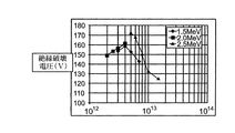
a)絶縁破壊電圧を上昇させ、かつON抵抗値を低下させる。
b)高電界領域をトレンチの角部から引き離すことにより、装置の信頼性を高めることができる。
c)ベースダイオード領域が後退して、積層欠陥等の欠損部が、漏洩電流の通り道となりうる高導電性接触領域に到達するのを防止し、ドレイン・ソース遮断電流(Idss)の漏洩を減少させることができる。
d)絶縁破壊電圧とドレイン・ソース遮断電流(Idss)をエッチングの深さの変動に影響されないようにすることにより、トレンチと接合領域をエッチングする際の制約を小さくすることができる。
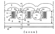
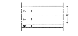
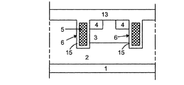
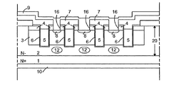
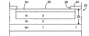
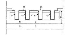
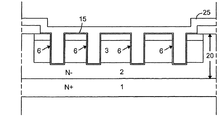
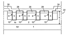
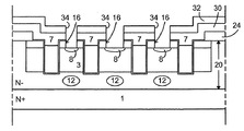
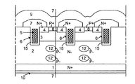
3 ベース領域
4 ソース領域
5 ゲート電極
6 トレンチ
7 絶縁中間層
8 高導電性接触領域
9 ソース接合部
10 ドレイン接合部
11 高導電性領域
12 電界救済領域
13 酸化物層
15 ゲート酸化膜
16 凹部
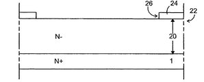
19 ウィンドー
20 エピタキシャル層
22 金型
23 ウィンドー
24 電界酸化膜層
25 ポリシリコン層
26 ウィンドー
28 ソース層
29 フォトレジスト層
30 酸化膜
32 フォトレジスト膜
34 ウィンドー
Claims (5)
- 第1の導電型の半導体基板と、
基板の上方に配置される、前記第1の導電型の共通導電領域と、
前記共通導電領域上に形成された第2の導電型のベース領域と、
前記ベース領域を経て前記共通導電領域まで下方に延びるように形成され、各トレンチは、少なくとも1つの側壁上に位置するゲート絶縁層を含み、かつ導電性のゲート材料により充填されるようになっている複数のトレンチと、
前記ベース領域の表面に、各々がトレンチに隣接するように形成された前記第1の導電型の複数のソース領域と、
前記ベース領域内に形成され、各前記トレンチの間の2つの前記ソース領域の間に位置する複数の高導電性接触領域と、
前記共通導電領域内に形成され、前記ベース領域の下方に延在する、前記第2の導電型の複数の電界救済領域と
を備え、
前記電界救済領域の各々は、少量のドーパントを有し、前記ベース領域及び前記トレンチから離間し、各々の前記高導電性接触領域に対してその下方に整列される
MOSゲート装置。 - 前記第1の導電型のソース領域とオーミック接合をなす第1の接合部も備えていることを特徴とする請求項1記載のMOSゲート装置。
- 前記複数の高導電性接触領域が、前記第2の導電型であり、かつ前記第1の接合部とオーミック接合をなすことを特徴とする請求項2記載のMOSゲート装置。
- 前記基板とオーミック接合をなす第2の接合部も備えていることを特徴とする請求項1記載のMOSゲート装置。
- 前記複数の電界救済領域よりも深い位置に形成された、もう1つの組をなす複数の電界救済領域を、さらに備えていることを特徴とする請求項1記載のMOSゲート装置。
Applications Claiming Priority (3)
| Application Number | Priority Date | Filing Date | Title |
|---|---|---|---|
| US37817302P | 2002-05-14 | 2002-05-14 | |
| US10/437,984 US7161208B2 (en) | 2002-05-14 | 2003-05-13 | Trench mosfet with field relief feature |
| PCT/US2003/015117 WO2003098663A2 (en) | 2002-05-14 | 2003-05-14 | Trench mosfet with field relief feature |
Publications (2)
| Publication Number | Publication Date |
|---|---|
| JP2005526392A JP2005526392A (ja) | 2005-09-02 |
| JP4201764B2 true JP4201764B2 (ja) | 2008-12-24 |
Family
ID=29423628
Family Applications (1)
| Application Number | Title | Priority Date | Filing Date |
|---|---|---|---|
| JP2004506063A Expired - Lifetime JP4201764B2 (ja) | 2002-05-14 | 2003-05-14 | 電界救済特性を有するトレンチ型mosfet |
Country Status (5)
| Country | Link |
|---|---|
| US (1) | US7161208B2 (ja) |
| EP (1) | EP1504474A4 (ja) |
| JP (1) | JP4201764B2 (ja) |
| AU (1) | AU2003251298A1 (ja) |
| WO (1) | WO2003098663A2 (ja) |
Families Citing this family (29)
| Publication number | Priority date | Publication date | Assignee | Title |
|---|---|---|---|---|
| US6916745B2 (en) * | 2003-05-20 | 2005-07-12 | Fairchild Semiconductor Corporation | Structure and method for forming a trench MOSFET having self-aligned features |
| JP2004335990A (ja) * | 2003-03-10 | 2004-11-25 | Fuji Electric Device Technology Co Ltd | Mis型半導体装置 |
| TWI222685B (en) * | 2003-12-18 | 2004-10-21 | Episil Technologies Inc | Metal oxide semiconductor device and fabricating method thereof |
| JP4813762B2 (ja) * | 2003-12-25 | 2011-11-09 | ルネサスエレクトロニクス株式会社 | 半導体装置及びその製造方法 |
| JP4564362B2 (ja) * | 2004-01-23 | 2010-10-20 | 株式会社東芝 | 半導体装置 |
| JP4454396B2 (ja) * | 2004-06-08 | 2010-04-21 | 株式会社ブリヂストン | 生タイヤの成型方法、およびそれに用いられる生タイヤ冷却装置 |
| GB0417749D0 (en) * | 2004-08-10 | 2004-09-08 | Eco Semiconductors Ltd | Improved bipolar MOSFET devices and methods for their use |
| JP2006332607A (ja) * | 2005-04-28 | 2006-12-07 | Nec Electronics Corp | 半導体装置 |
| JP2007005657A (ja) * | 2005-06-24 | 2007-01-11 | Nec Electronics Corp | 半導体装置及び半導体装置の製造方法 |
| JP2007027193A (ja) * | 2005-07-12 | 2007-02-01 | Renesas Technology Corp | 半導体装置およびその製造方法、ならびに非絶縁型dc/dcコンバータ |
| JP2008098530A (ja) * | 2006-10-13 | 2008-04-24 | Toshiba Corp | 半導体装置の製造方法 |
| JP2008108962A (ja) * | 2006-10-26 | 2008-05-08 | Toshiba Corp | 半導体装置 |
| EP2093802B1 (en) * | 2006-12-04 | 2015-11-11 | Sanken Electric Co., Ltd. | Insulating-gate fet and its manufacturing method |
| JP4564514B2 (ja) * | 2007-05-18 | 2010-10-20 | 株式会社東芝 | 半導体装置 |
| US7875951B2 (en) * | 2007-12-12 | 2011-01-25 | Infineon Technologies Austria Ag | Semiconductor with active component and method for manufacture |
| JP5526496B2 (ja) * | 2008-06-02 | 2014-06-18 | サンケン電気株式会社 | 電界効果半導体装置及びその製造方法 |
| JP5136674B2 (ja) * | 2010-07-12 | 2013-02-06 | 株式会社デンソー | 半導体装置およびその製造方法 |
| JP2012043955A (ja) * | 2010-08-18 | 2012-03-01 | Toshiba Corp | 半導体装置及びその製造方法 |
| JP6290526B2 (ja) | 2011-08-24 | 2018-03-07 | ローム株式会社 | 半導体装置およびその製造方法 |
| JP5763514B2 (ja) * | 2011-12-13 | 2015-08-12 | トヨタ自動車株式会社 | スイッチング素子の製造方法 |
| CN104106142B (zh) * | 2012-02-10 | 2016-03-09 | 松下知识产权经营株式会社 | 半导体装置及其制造方法 |
| CN104810408A (zh) * | 2014-01-24 | 2015-07-29 | 无锡华润华晶微电子有限公司 | 一种超势垒整流器件及其制造方法 |
| JP2017112161A (ja) * | 2015-12-15 | 2017-06-22 | 三菱電機株式会社 | 半導体装置 |
| CN108604603B (zh) * | 2016-02-02 | 2021-05-28 | Abb电网瑞士股份公司 | 功率半导体装置 |
| JP7238828B2 (ja) * | 2020-02-14 | 2023-03-14 | 豊田合成株式会社 | 半導体素子の製造方法 |
| CN111293174A (zh) * | 2020-02-25 | 2020-06-16 | 英诺赛科(珠海)科技有限公司 | 半导体器件及其制造方法 |
| CN113808946B (zh) * | 2020-06-12 | 2026-03-17 | 芯恩(青岛)集成电路有限公司 | 超结功率器件及其制备方法 |
| CN113808945B (zh) * | 2020-06-12 | 2024-11-26 | 芯恩(青岛)集成电路有限公司 | 超结功率器件及其制备方法 |
| CN113990935A (zh) * | 2021-11-25 | 2022-01-28 | 芜湖启迪半导体有限公司 | 一种沟槽碳化硅mosfet器件及其制备方法 |
Family Cites Families (26)
| Publication number | Priority date | Publication date | Assignee | Title |
|---|---|---|---|---|
| US5034785A (en) | 1986-03-24 | 1991-07-23 | Siliconix Incorporated | Planar vertical channel DMOS structure |
| US4767722A (en) | 1986-03-24 | 1988-08-30 | Siliconix Incorporated | Method for making planar vertical channel DMOS structures |
| US4967245A (en) | 1988-03-14 | 1990-10-30 | Siliconix Incorporated | Trench power MOSFET device |
| US5072266A (en) | 1988-12-27 | 1991-12-10 | Siliconix Incorporated | Trench DMOS power transistor with field-shaping body profile and three-dimensional geometry |
| US5910669A (en) | 1992-07-24 | 1999-06-08 | Siliconix Incorporated | Field effect Trench transistor having lightly doped epitaxial region on the surface portion thereof |
| US5665996A (en) | 1994-12-30 | 1997-09-09 | Siliconix Incorporated | Vertical power mosfet having thick metal layer to reduce distributed resistance |
| US5674766A (en) | 1994-12-30 | 1997-10-07 | Siliconix Incorporated | Method of making a trench MOSFET with multi-resistivity drain to provide low on-resistance by varying dopant concentration in epitaxial layer |
| US5592005A (en) | 1995-03-31 | 1997-01-07 | Siliconix Incorporated | Punch-through field effect transistor |
| JP3158973B2 (ja) * | 1995-07-20 | 2001-04-23 | 富士電機株式会社 | 炭化けい素縦型fet |
| US6037632A (en) * | 1995-11-06 | 2000-03-14 | Kabushiki Kaisha Toshiba | Semiconductor device |
| US6090716A (en) | 1996-12-17 | 2000-07-18 | Siliconix Incorporated | Method of fabricating a field effect transistor |
| US6342709B1 (en) * | 1997-12-10 | 2002-01-29 | The Kansai Electric Power Co., Inc. | Insulated gate semiconductor device |
| DE19816448C1 (de) * | 1998-04-14 | 1999-09-30 | Siemens Ag | Universal-Halbleiterscheibe für Hochspannungs-Halbleiterbauelemente, ihr Herstellungsverfahren und ihre Verwendung |
| JP3988262B2 (ja) * | 1998-07-24 | 2007-10-10 | 富士電機デバイステクノロジー株式会社 | 縦型超接合半導体素子およびその製造方法 |
| EP2261961B1 (de) * | 1999-03-04 | 2019-07-17 | Infineon Technologies AG | Verfahren zur Herstellung einer vertikalen MOS-Transistoranordnung |
| GB9906247D0 (en) | 1999-03-18 | 1999-05-12 | Koninkl Philips Electronics Nv | An electronic device comprising a trench gate field effect device |
| US6188105B1 (en) * | 1999-04-01 | 2001-02-13 | Intersil Corporation | High density MOS-gated power device and process for forming same |
| JP2006210368A (ja) * | 1999-07-02 | 2006-08-10 | Toyota Central Res & Dev Lab Inc | 縦型半導体装置及びその製造方法 |
| US6211018B1 (en) * | 1999-08-14 | 2001-04-03 | Electronics And Telecommunications Research Institute | Method for fabricating high density trench gate type power device |
| DE19947020B4 (de) * | 1999-09-30 | 2006-02-23 | Infineon Technologies Ag | Kompensationsbauelement mit variabler Ladungsbilanz und dessen Herstellungsverfahren |
| US6534828B1 (en) | 2000-09-19 | 2003-03-18 | Fairchild Semiconductor Corporation | Integrated circuit device including a deep well region and associated methods |
| KR100385859B1 (ko) * | 2000-12-27 | 2003-06-02 | 한국전자통신연구원 | 트렌치 게이트 mosfet 전력소자 제조방법 |
| JP3506676B2 (ja) * | 2001-01-25 | 2004-03-15 | Necエレクトロニクス株式会社 | 半導体装置 |
| US7045859B2 (en) * | 2001-09-05 | 2006-05-16 | International Rectifier Corporation | Trench fet with self aligned source and contact |
| US6465304B1 (en) * | 2001-10-04 | 2002-10-15 | General Semiconductor, Inc. | Method for fabricating a power semiconductor device having a floating island voltage sustaining layer |
| US7701001B2 (en) * | 2002-05-03 | 2010-04-20 | International Rectifier Corporation | Short channel trench power MOSFET with low threshold voltage |
-
2003
- 2003-05-13 US US10/437,984 patent/US7161208B2/en not_active Expired - Lifetime
- 2003-05-14 EP EP03753029A patent/EP1504474A4/en not_active Ceased
- 2003-05-14 AU AU2003251298A patent/AU2003251298A1/en not_active Abandoned
- 2003-05-14 WO PCT/US2003/015117 patent/WO2003098663A2/en not_active Ceased
- 2003-05-14 JP JP2004506063A patent/JP4201764B2/ja not_active Expired - Lifetime
Also Published As
| Publication number | Publication date |
|---|---|
| EP1504474A2 (en) | 2005-02-09 |
| WO2003098663A2 (en) | 2003-11-27 |
| US7161208B2 (en) | 2007-01-09 |
| JP2005526392A (ja) | 2005-09-02 |
| US20030213993A1 (en) | 2003-11-20 |
| AU2003251298A8 (en) | 2003-12-02 |
| EP1504474A4 (en) | 2006-12-06 |
| AU2003251298A1 (en) | 2003-12-02 |
| WO2003098663A3 (en) | 2004-12-09 |
Similar Documents
| Publication | Publication Date | Title |
|---|---|---|
| JP4201764B2 (ja) | 電界救済特性を有するトレンチ型mosfet | |
| US7821063B2 (en) | Semiconductor device having enhanced performance and method | |
| US11545569B2 (en) | Method of fabricating a field-effect transistor | |
| JP2007515079A (ja) | 従来の端子を備えた超接合装置の製造方法 | |
| KR20010023861A (ko) | 반도체 전력 장치의 제조 방법 | |
| JP2010021176A (ja) | 半導体装置および半導体装置の製造方法 | |
| JP5048214B2 (ja) | 低閾値電圧を有する短チャンネルトレンチパワーmosfet | |
| US9853099B1 (en) | Double diffused metal oxide semiconductor device and manufacturing method thereof | |
| US7696061B2 (en) | Semiconductor device and method for manufacturing same | |
| JP4800566B2 (ja) | 半導体装置及びその製造方法 | |
| US7629645B2 (en) | Folded-gate MOS transistor | |
| US8421149B2 (en) | Trench power MOSFET structure with high switching speed and fabrication method thereof | |
| US20240234495A1 (en) | Gate trench power semiconductor devices having self-aligned trench shielding regions and related methods | |
| KR101044778B1 (ko) | 비대칭 고전압 트랜지스터 및 그 제조방법 | |
| KR101177485B1 (ko) | 매립 게이트형 반도체 소자 및 그 제조방법 | |
| TWI523229B (zh) | 一種溝槽式功率半導體結構之製造方法 | |
| KR100649836B1 (ko) | 반도체 소자의 제조 방법 | |
| JP2006332231A (ja) | 半導体装置の製造方法 | |
| HK1107445B (en) | Power semiconductor device having improved performance and method | |
| HK1107445A1 (en) | Power semiconductor device having improved performance and method | |
| KR20080114222A (ko) | 반도체 소자 및 그 제조 방법 | |
| KR20060075000A (ko) | 반도체 메모리 소자의 트랜지스터 및 그 제조 방법 |
Legal Events
| Date | Code | Title | Description |
|---|---|---|---|
| A977 | Report on retrieval |
Free format text: JAPANESE INTERMEDIATE CODE: A971007 Effective date: 20070223 |
|
| A131 | Notification of reasons for refusal |
Free format text: JAPANESE INTERMEDIATE CODE: A131 Effective date: 20070306 |
|
| A601 | Written request for extension of time |
Free format text: JAPANESE INTERMEDIATE CODE: A601 Effective date: 20070605 |
|
| A602 | Written permission of extension of time |
Free format text: JAPANESE INTERMEDIATE CODE: A602 Effective date: 20070612 |
|
| A521 | Request for written amendment filed |
Free format text: JAPANESE INTERMEDIATE CODE: A523 Effective date: 20070903 |
|
| A131 | Notification of reasons for refusal |
Free format text: JAPANESE INTERMEDIATE CODE: A131 Effective date: 20071106 |
|
| A521 | Request for written amendment filed |
Free format text: JAPANESE INTERMEDIATE CODE: A523 Effective date: 20080205 |
|
| A131 | Notification of reasons for refusal |
Free format text: JAPANESE INTERMEDIATE CODE: A131 Effective date: 20080415 |
|
| A601 | Written request for extension of time |
Free format text: JAPANESE INTERMEDIATE CODE: A601 Effective date: 20080715 |
|
| A521 | Request for written amendment filed |
Free format text: JAPANESE INTERMEDIATE CODE: A523 Effective date: 20080716 |
|
| A602 | Written permission of extension of time |
Free format text: JAPANESE INTERMEDIATE CODE: A602 Effective date: 20080723 |
|
| TRDD | Decision of grant or rejection written | ||
| A01 | Written decision to grant a patent or to grant a registration (utility model) |
Free format text: JAPANESE INTERMEDIATE CODE: A01 Effective date: 20080930 |
|
| A01 | Written decision to grant a patent or to grant a registration (utility model) |
Free format text: JAPANESE INTERMEDIATE CODE: A01 |
|
| A61 | First payment of annual fees (during grant procedure) |
Free format text: JAPANESE INTERMEDIATE CODE: A61 Effective date: 20081007 |
|
| R150 | Certificate of patent or registration of utility model |
Ref document number: 4201764 Country of ref document: JP Free format text: JAPANESE INTERMEDIATE CODE: R150 Free format text: JAPANESE INTERMEDIATE CODE: R150 |
|
| FPAY | Renewal fee payment (event date is renewal date of database) |
Free format text: PAYMENT UNTIL: 20111017 Year of fee payment: 3 |
|
| FPAY | Renewal fee payment (event date is renewal date of database) |
Free format text: PAYMENT UNTIL: 20121017 Year of fee payment: 4 |
|
| R250 | Receipt of annual fees |
Free format text: JAPANESE INTERMEDIATE CODE: R250 |
|
| FPAY | Renewal fee payment (event date is renewal date of database) |
Free format text: PAYMENT UNTIL: 20131017 Year of fee payment: 5 |
|
| R250 | Receipt of annual fees |
Free format text: JAPANESE INTERMEDIATE CODE: R250 |
|
| R250 | Receipt of annual fees |
Free format text: JAPANESE INTERMEDIATE CODE: R250 |
|
| R250 | Receipt of annual fees |
Free format text: JAPANESE INTERMEDIATE CODE: R250 |
|
| R250 | Receipt of annual fees |
Free format text: JAPANESE INTERMEDIATE CODE: R250 |
|
| R250 | Receipt of annual fees |
Free format text: JAPANESE INTERMEDIATE CODE: R250 |
|
| R250 | Receipt of annual fees |
Free format text: JAPANESE INTERMEDIATE CODE: R250 |
|
| S531 | Written request for registration of change of domicile |
Free format text: JAPANESE INTERMEDIATE CODE: R313531 |
|
| S533 | Written request for registration of change of name |
Free format text: JAPANESE INTERMEDIATE CODE: R313533 |
|
| R350 | Written notification of registration of transfer |
Free format text: JAPANESE INTERMEDIATE CODE: R350 |
|
| R250 | Receipt of annual fees |
Free format text: JAPANESE INTERMEDIATE CODE: R250 |
|
| R250 | Receipt of annual fees |
Free format text: JAPANESE INTERMEDIATE CODE: R250 |
|
| R250 | Receipt of annual fees |
Free format text: JAPANESE INTERMEDIATE CODE: R250 |
|
| R250 | Receipt of annual fees |
Free format text: JAPANESE INTERMEDIATE CODE: R250 |
|
| R250 | Receipt of annual fees |
Free format text: JAPANESE INTERMEDIATE CODE: R250 |
|
| EXPY | Cancellation because of completion of term |