JP4222678B2 - Current measuring device - Google Patents
Current measuring device Download PDFInfo
- Publication number
- JP4222678B2 JP4222678B2 JP10237599A JP10237599A JP4222678B2 JP 4222678 B2 JP4222678 B2 JP 4222678B2 JP 10237599 A JP10237599 A JP 10237599A JP 10237599 A JP10237599 A JP 10237599A JP 4222678 B2 JP4222678 B2 JP 4222678B2
- Authority
- JP
- Japan
- Prior art keywords
- circuit
- current
- measurement
- terminal
- amplifier
- Prior art date
- Legal status (The legal status is an assumption and is not a legal conclusion. Google has not performed a legal analysis and makes no representation as to the accuracy of the status listed.)
- Expired - Fee Related
Links
Images
Landscapes
- Measurement Of Resistance Or Impedance (AREA)
- Measurement Of Current Or Voltage (AREA)
Description
【0001】
【発明の属する技術分野】
本発明は、各種直流回路の直流回路電流を、回路を切断することなく、あるいはクランプセンサ等を使用することなく、簡便に測定する装置に関するものであり、詳しくはバッテリ等の電源回路電流やプリント板内の回路電流、プロセスオートメーションにおける各種センサーの直流出力電流4−20mA等を、回路を切断することなく、プローブを接触させるだけで測定できるようにした装置に関するものである。
【0002】
【従来の技術】
従来より、直流回路の電流を測定するには通常次の方式がある。
(1) 回路を切断して電流計を挿入し、そこに流れる電流を測定する方式。
(2) 直流クランプセンサを用い、回路を切断しないで電流を測定する方式。
【0003】
【発明が解決しようとする課題】
ところで、上記方式では次のような課題がある。すなわち、
▲1▼上記(1) の方式では回路を切断する必要があり、特にプリント板回路の場合には好ましい方式とは言えない。
▲2▼上記(2) の方式では、微小電流測定において感度的に限界がある。また回路がクランプセンサでクランプできる形状(ワイヤまたはブスバー)でなければならず、例えばプリント板パターン上の電流は測定できない。
【0004】
本発明の目的は、このような課題を解決するもので、非切断で直流回路電流を高感度に測定することのできる電流測定装置を実現することにある。
【0005】
【課題を解決するための手段】
このような目的を達成するために請求項1の発明では、
4端子構造の測定端子を用い、この測定端子の電流端子より被測定対象の低抵抗回路に交流の定電流を印加する交流定電流源と、
前記測定端子の電圧端子より交流信号の電圧降下を検出し、この検出信号を交流アンプで増幅後、同期整流により前記交流信号成分に同期した信号のみを検出して前記低抵抗回路の抵抗値を測定する抵抗測定手段と、
前記測定端子間に生ずる微小直流電圧降下を直流アンプにより検出し、この検出信号をフィルタに通して前記交流信号成分を除去し測定端子間の直流電圧降下を測定する電圧降下測定手段と、
前記抵抗測定手段と電圧降下測定手段の各出力をデジタル変換し、そのデジタルデータをもとに演算により前記測定端子の2点間に流れる被測定対象の直流回路電流値を求め、この求めた直流回路電流を表示するように構成された手段
を具備し、前記被測定対象の回路を切断することなく直流回路電流を測定できるように構成したことを特徴とする。
【0006】
この発明では、被測定対象の低抵抗回路に測定端子の電流端子より交流の定電流を印加した状態において、測定端子の電圧端子より交流信号の電圧降下を検出し、この検出信号を増幅後、印加交流成分に同期した信号のみ同期整流・検出する。次に、電圧端子間に生ずる微小直流電圧降下を高感度直流アンプとフィルタを介して検出する。
【0007】
そしてこの2つの検出信号を交互にA−D変換し、その変換データをもとに演算により、電流値(mA)=直流電圧降下(μV)/直流抵抗値(mΩ)を求めて、測定端子間の電流値(mA)を得る。
このようにして、被測定対象の回路(導線)を切断することなく回路電流を求めることができる。
【0008】
また、請求項2のように、
4端子構造の測定端子を用い、この測定端子の電流端子より被測定対象の低抵抗回路に交流の定電流を印加する交流定電流源と、
前記測定端子の電圧端子より交流信号の電圧降下を検出し、この検出信号を交流アンプで増幅後、同期整流により前記交流信号成分に同期した信号のみを検出して前記低抵抗回路の抵抗値を測定する抵抗測定手段と、
前記測定端子間に生ずる微小直流電圧降下を直流アンプにより検出し、この検出信号をフィルタに通して前記交流信号成分を除去し測定端子間の直流電圧降下を測定する電圧降下測定手段と、
前記抵抗測定手段と電圧降下測定手段の各出力をデジタル変換し、そのデジタルデータをもとに演算により前記測定端子の2点間に流れる被測定対象の直流回路電流値を求め、この求めた直流回路電流を表示するように構成された手段と、
前記抵抗測定手段の交流アンプと前記電圧降下測定手段の直流アンプを共通化して1系統の構成とすると共に、その出力を平均化する平均化回路より構成し、
抵抗測定モードにおいては、直流分を阻止すると共に、前記印加する交流定電流の周波数の半周期ごとに信号を反転させて前記平均化回路に印加することにより同期整流を構成して直流抵抗分に比例した出力を得るようにし、
直流電圧測定モードにおいては、前記半周期ごとの反転切換えを止めて単なるフィルタ回路が構成されるようにし、
前記抵抗測定モードと直流電圧測定モードを切換えて前記測定端子間の直流低抵抗と直流微小電圧降下を交互に測定するように構成することもできる。
【0009】
また、請求項3の発明では、
4端子構造の測定端子を用い、この測定端子の2点間に生じた被測定対象の低抵抗回路における電圧降下を検出するアンプと、
このアンプの出力電圧で駆動され前記測定端子の電流端子より前記電圧降下がゼロとなるように被測定対象に電流を供給する電流発生回路と、
前記アンプの出力が安定した状態のときのアンプ出力を読み取って前記測定端子の2点間に流れる被測定対象の回路電流を求める手段を具備し、
前記被測定対象の回路を切断することなく回路電流を測定できるように構成したことを特徴とする。
【0010】
このような構成では、回路抵抗による電圧降下を直流アンプで検出し、その出力で駆動される直流電流発生回路より測定端子の電流端子に電流を印加し、電圧降下がゼロになるように電流発生回路を制御する。制御が安定した状態における電流発生回路の出力電流から回路電流を求めることができる。
【0011】
ただし、ここでは電流発生回路の出力電流が直流アンプの出力電圧に対応しているので、直流アンプの出力電圧の測定をもって回路電流を求めるようにしている。このような構成によれば、構成が簡単であるばかりでなく、零位法により容易に高精度の測定が可能であるという利点がある。
【0012】
【発明の実施の形態】
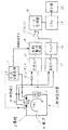
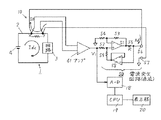
以下図面を用いて本発明を詳しく説明する。本発明は4端子構造の測定端子を用いて被測定回路の電流を測定する方式であり、図1は本発明に係る電流測定装置の一実施例を示す構成図である。
【0013】
図1において、測定端子10は2つの電圧端子と2つの電流端子からなる4端子構造の測定端子であり、測定時には電圧端子の外側に電流端子が接続されるように被測定対象1の導線2の測定点x,yの2点にそれぞれ接続される。
被測定対象1としては例えば回路3と電池4を導線2で接続したものである。
【0014】
交流定電流源11は測定端子10の電流端子に周波数fの交流定電流を供給する。交流アンプ13は交流電圧を適宜増幅するもので、コンデンサ12で直流カットされた測定端子10からの電圧信号を受けて適宜増幅する。同期整流回路14は交流アンプ14の出力を交流定電流源11の周波数fの交流信号成分で同期整流する。
【0015】
なお、コンデンサ12、交流アンプ13および同期整流回路14からなる部分は、測定端子により検出された信号から被測定対象の測定端子間の回路抵抗を測定するための回路部分であり、ここではこれを抵抗測定手段と呼ぶ。
【0016】
直流アンプ15は測定端子10の電圧端子からの電圧信号を増幅する。フィルタ16はその増幅信号から交流成分を除去する(主として周波数fの信号成分を除去する)。
なお、直流アンプ15およびフィルタ16からなる部分は、入力信号から交流信号成分を除去し測定端子間の直流電圧降下を検出するものであり、ここではこれを電圧降下測定手段と呼ぶ。
【0017】
スイッチ17は同期整流回路14とフィルタ16の出力を択一的に選択する。アナログ・デジタル変換器(以下アナログ・デジタル変換をA−D変換という)18はアナログ信号をデジタル信号に変換するもので、スイッチ17の出力をデジタル信号に変換する。
【0018】
中央処理装置(以下単にCPUという)19は所定の演算処理および各部の制御を行う機能を有する。表示器20はCPU19での演算結果を表示する。
【0019】
このような構成における動作を次に説明する。4端子構造の測定端子10を被測定対象1の測定点x、yの2点に接続する。交流定電流源11より電流端子に周波数fの交流定電流を供給し、x、y間の回路抵抗rに比例する電圧降下を電圧端子により検出する。この電圧信号をコンデンサ12に通して交流成分のみ取り出し交流アンプ13で適宜増幅し、同期整流回路14でこれを周波数fに同期整流し印加交流成分に同期した信号のみを取り出す。
【0020】
この同期整流出力は直流抵抗r(低抵抗)に比例した電圧である。この電圧信号はスイッチ17経由でA−D変換器18に送られ、デジタル変換され、CPU19に読み取られる。
【0021】
次に、被測定対象1の測定点x、yの2点間の直流電圧降下Vdcを電圧端子で検出し、直流アンプ15でこれを増幅し、続いてフィルタ16で交流成分を除去した後スイッチ17経由でA−D変換器18でデジタル変換する。デジタル変換された電圧降下の値はCPU19に読み取られる。
【0022】
CPU19は、上記2つのデータ、すなわち直流抵抗r(例えばmΩ)に比例した電圧値と直流電圧降下Vdc(例えばμV)に比例した電圧値をもとに、次式の演算により測定点x、y間の直流電流Idc(mA)を求める。
Idc=Vdc/r
このようにして得られた直流電流IdcはCPU19の制御により表示器20に表示される。
【0023】
このように、回路抵抗rとそのrに生ずる電圧降下Vdcを正確に捉えることができ、回路を切断することなく回路電流を計測することができる。
【0024】
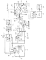
図2は本発明の他の実施例を示す構成図である。図2において図1と同等部分には同一符号を付してある。
【0025】
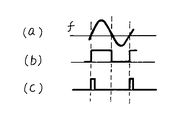
波形整形回路21は図3の(a)に示す交流定電流源11の同期信号(周波数fの交流電流信号)を波形整形し、図3の(b)に示すようなパルス幅が同期信号の半周期幅であるパルス信号を発生する。
パルス発生器22は、図3の(c)に示すように波形整形回路21の出力パルスの立ち上がりに同期したパルスを発生する。
【0026】
アンプ23は測定端子10で検出した電圧信号を適宜増幅するもので、ここでは演算増幅器231と抵抗232,233より構成された一般的な増幅回路が使用されている。この演算増幅器231の非反転入力端は、オートゼロ回路24を介して測定端子10の一方の端子またはコモンラインに接続されている。また演算増幅器231の反転入力端は、自身の出力端とコモンライン間に接続された直列接続抵抗232,233の共通接続点に接続されている。なお、測定端子10の他方の端子はコモンラインに接続されている。
【0027】
オートゼロ回路24はアンプ23の入力を切り替えるもので、通常測定時にはアンプ23の非反転入力端を測定端子10に接続し、ゼロ点補正時には非反転入力端をコモンラインに接続するものである。
【0028】
反転回路27はアンプ23の出力信号を反転する回路で、ここでは演算増幅器271と入力抵抗272、帰還抵抗273より構成された一般的な反転増幅回路が使用されている。
【0029】
切換スイッチ28(S2,S3)は、アンプ23の出力またはその反転出力のいずれかを波形整形回路21の出力パルスの状態に関連して選択する。なお、この場合、アンプ23の出力はコンデンサ25を介して出力される。ただし、直流電圧測定モード時には、コンデンサ25に並列接続されたオン・オフスイッチ26(S1)がオンとなり、コンデンサ25は短絡状態となる。
【0030】
なお、アンプ23、コンデンサ25、スイッチ26、反転回路27、スイッチ28からなる部分を、ここでは信号選択手段と呼ぶ。
【0031】
積分器30は、スイッチ28から抵抗29を介して入力される電流を積分する。その積分電圧は、スイッチ311(S4)とコンデンサ312でなるサンプルホールド回路31によりサンプルホールドされる。
【0032】
コンデンサ312にホールドされた電圧は、トランジスタ33のコレクタ・ベース間に接続されたFET32のゲートに入力される。トランジスタ33のエミッタは抵抗34を介して低電圧源に接続され、コレクタは高電圧源にそれぞれ接続されている。また、トランジスタ33のエミッタは抵抗35を介して積分器30の入力端に接続されている。
このトランジスタ33のエミッタからはコンデンサ312のホールド電圧に対応した電圧が得られ、その電圧信号は、A−D変換器18でデジタル変換される。
【0033】
このような構成における動作を次に説明する。4端子構造の測定端子10を被測定対象1の測定点x、yの2点に接続する。以下2点間の抵抗を測定する抵抗測定モードと、2点間の電圧を測定する電圧測定モードとに分けて説明する。
【0034】
(1) 抵抗測定モード
交流定電流源11より電流端子に周波数fの交流定電流を供給し、x、y間の回路抵抗rに比例する電圧降下を電圧端子により検出する。オートゼロ回路24は測定端子10がアンプ23の入力端に接続されるように設定しておく。
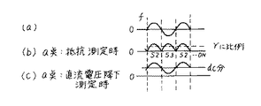
前記検出信号をアンプ23で適宜に増幅した後コンデンサ25で直流成分を除去し直流成分の除去された信号vを得る。スイッチ28では前記交流定電流印加の半周期ごとに信号vと反転信号−vを交互に選択し、図4の(b)に示すような波形を得て、これを抵抗29を介して積分器30に印加して積分する。
【0035】
積分出力を前記交流定電流印加の1周期ごとにサンプルホールドすることにより同期整流と交流信号成分の除去が行われ、トランジスタ33のエミッタからは回路抵抗rに比例した出力電圧が得られる。
【0036】
(2) 直流電圧測定モード
抵抗測定モードの場合と同様に、交流定電流源11より電流端子に周波数fの交流定電流を供給したまま、x、y間の回路抵抗rに比例する直流電圧降下を電圧端子により検出する。オートゼロ回路24は測定端子10がアンプ23の入力端に接続されるように設定しておく。
【0037】
更に、スイッチ26をオンにしてコンデンサ25を短絡すると共に、スイッチ28のS2をオンにして、アンプ23の出力vのみが積分されるように設定する。この場合、アンプ23の出力vは図4の(c)に示すように直流分に交流が重畳した波形である。
【0038】
積分出力を前記交流定電流印加の1周期ごとにサンプルホールドすることにより直流分に重畳されている交流分がフィルター効果で除去され、直流電圧降下Vdcを検出することができる。
【0039】
このようにして回路抵抗rと、そのrに生ずる電圧降下Vdcを正確に捉えることができ、回路を切断することなく回路電流を計測することができる。
【0040】
なお、電圧測定モードにおいて、オートゼロ回路24を切換えてアンプ23の入力を短絡してオフセット分を測定しておき、CPU19での演算の際にゼロ補正を行えば、より高精度の測定が可能となる。
ただし、このゼロ補正は本発明に必須の事項ではない。
【0041】
また、平均化回路としては、必ずしも実施例のように積分器とサンプルホールド回路で構成した回路である必要はなく、通常のフィルターを使用したものでもよい。通常のフィルターを使用しても本発明の本質に変わりはない。
【0042】
図5は本発明の更に他の実施例を示す構成図である。4端子構造の測定端子10で検出された信号は、利得が十分に大きいアンプ41で増幅される。直流電流発生回路50はアンプ41の出力電圧v1に対応した電流Ioを発生する。その電流は測定端子10を介して2点間x,yに印加される。この場合、電流Ioは被測定対象1に流れる電流Idcとは逆極性となるように加えられる。
【0043】
電流発生回路50は、例えば次のような構成のものが使用される。演算増幅器51の非反転入力端に入力抵抗52が接続され、演算増幅器51の反転入力端には帰還抵抗53が接続されると共に、他方がコモンラインに接続された抵抗54が接続されている。演算増幅器51の出力は抵抗55(抵抗値R)を介して出力端子56に接続されている。
【0044】
また、出力端子56の電圧はバッファアンプ58を経由し、抵抗59を介して演算増幅器51の非反転入力端に加えられている。
そして、出力端子56,57は4端子構造の電流端子に接続されている。
【0045】
さて、図5のような構成においては、電流発生回路50から出力される電流Ioがx、yの2点間に加えられるが、このときx、y間の電圧がゼロとなるように、すなわちアンプ41が制御用誤差増幅器の役割となって、Idcと逆極性の電流Ioが流れx、y間の電圧がゼロとなるように制御される。
【0046】
この場合の電流発生回路50の入力v1と出力Ioとの関係は
Io=k・v1/R
ただし、kは比例定数
で与えられ、平衡した状態のv1を知ることによりIoすなわちIdcを求めることができる。
【0047】
アンプ41の出力v1の値はA−D変換器18でデジタル変換され、CPU19ではこれを読み取って上記の関係式に基づき演算により回路電流Idcを求め、表示器20に表示する。
【0048】
図1および図2に示す電流測定装置の測定方法は偏移法であるのに対し、図5に示す電流測定装置は零位法に相当する。この方法は測定すべき回路電流と同じ出力電流を供給する必要があるが、零位法であるためより高精度が期待できる。
【0049】
以上のような本発明の電流測定装置を使用して例えばプリント板上の回路電流を測定する場合、パターン抵抗は10mΩ程度以上あるから直流電圧検出感度を0.1μVとすると、0.01mAの電流検出感度が得られ、実用上十分な感度が得られる。バッテリ回路等の大電流・低抵抗回路の場合でも、測定端子接続の2点間の電圧降下が100μV程度あれば、十分実用に供せられる。
【0050】
ただし、直流電圧測定の場合は熱起電力の影響を受けるため、2点間の温度分布が一様でないときは測定端子の正負を入れ換えて平均化するなどの工夫が必要となる。
【0051】
なお、以上の説明は、本発明の説明および例示を目的として特定の好適な実施例を示したに過ぎない。したがって本発明は、上記実施例に限定されることなく、その本質から逸脱しない範囲で更に多くの変更、変形をも含むものである。
【0052】
【発明の効果】
以上説明したように本発明によれば、少なくともクランプセンサで測定するよりも高感度化が可能であり、磁界の影響を受けず、しかもクランプセンサ方式では不可能な非切断での電流測定が可能である等の利点があり、実用に供してその効果は大である。
また、本発明は、製品形態としては、回路電流を測定する電流計または低抵抗を測定する低抵抗測定器(いわゆるmΩメータ)、あるいはその両用が可能である。
【図面の簡単な説明】
【図1】 本発明に係る電流測定装置の一実施例を示す構成図である。
【図2】 本発明に係る電流測定装置の他の実施例を示す構成図である。
【図3】 動作説明用の各部の波形を示す図である。
【図4】 各モードにおける検出信号の波形を説明するための図である。
【図5】 本発明に係る電流測定装置の更に他の実施例を示す構成図である。
【符号の説明】
1 被測定対象
2 導線
3 回路
4 電池
10 測定端子
11 交流定電流源
12,25 コンデンサ
13 交流アンプ
14 同期整流回路
15 直流アンプ
16 フィルタ
17,26,28 スイッチ
18 A−D変換器
19 CPU
20 表示器
21 波形整形回路
22 パルス発生器
23,41 アンプ
24 オートゼロ回路
27 反転回路
28 切換スイッチ
29,34,35 抵抗
30 積分器
31 サンプルホールド回路
32 FET
33 トランジスタ
50 電流発生回路
51 演算増幅器
52,53,54,55,59 抵抗
58 バッファアンプ[0001]
BACKGROUND OF THE INVENTION
The present invention relates to an apparatus for easily measuring the DC circuit current of various DC circuits without cutting the circuit or using a clamp sensor or the like. The present invention relates to a device that can measure a circuit current in a board, a DC output current 4-20 mA of various sensors in process automation, and the like by simply contacting a probe without cutting the circuit.
[0002]
[Prior art]
Conventionally, there are usually the following methods for measuring the current of a DC circuit.
(1) A system that cuts the circuit and inserts an ammeter to measure the current flowing through it.
(2) A method that uses a DC clamp sensor to measure current without disconnecting the circuit.
[0003]
[Problems to be solved by the invention]
However, the above method has the following problems. That is,
{Circle around (1)} In the method (1), it is necessary to cut the circuit, which is not a preferable method particularly in the case of a printed circuit board.
(2) The above method (2) has a limit in sensitivity in the measurement of minute current. Further, the circuit must have a shape (wire or bus bar) that can be clamped by a clamp sensor, and for example, current on a printed board pattern cannot be measured.
[0004]
An object of the present invention is to solve such a problem and to provide a current measuring device capable of measuring a DC circuit current with high sensitivity without cutting.
[0005]
[Means for Solving the Problems]
In order to achieve such an object, the invention of
An AC constant current source that applies a constant AC current to a low resistance circuit to be measured from a current terminal of the measurement terminal using a measurement terminal having a four-terminal structure;
The voltage drop of the AC signal is detected from the voltage terminal of the measurement terminal, and after the detection signal is amplified by an AC amplifier, only the signal synchronized with the AC signal component is detected by synchronous rectification and the resistance value of the low resistance circuit is obtained. A resistance measuring means for measuring;
A voltage drop measuring means for detecting a minute DC voltage drop generated between the measurement terminals by a DC amplifier, passing the detection signal through a filter to remove the AC signal component, and measuring a DC voltage drop between the measurement terminals;
The respective outputs of the resistance measuring means and the voltage drop measuring means are converted into digital values, and a DC circuit current value of the measurement target flowing between two points of the measurement terminal is obtained by calculation based on the digital data. Means is provided for displaying the circuit current, and the DC circuit current can be measured without disconnecting the circuit to be measured.
[0006]
In this invention, in a state where an AC constant current is applied from the current terminal of the measurement terminal to the low resistance circuit to be measured, the voltage drop of the AC signal is detected from the voltage terminal of the measurement terminal, and after the detection signal is amplified, Synchronous rectification and detection only for signals synchronized with the applied AC component. Next, a minute DC voltage drop generated between the voltage terminals is detected through a high sensitivity DC amplifier and a filter.
[0007]
Then, these two detection signals are alternately A / D converted, and a current value (mA) = DC voltage drop (μV) / DC resistance value (mΩ) is obtained by calculation based on the converted data, and a measurement terminal A current value (mA) is obtained.
In this way, the circuit current can be obtained without cutting the circuit (conductor) to be measured.
[0008]
Further, as in
An AC constant current source that applies a constant AC current to a low resistance circuit to be measured from a current terminal of the measurement terminal using a measurement terminal having a four-terminal structure;
The voltage drop of the AC signal is detected from the voltage terminal of the measurement terminal, and after the detection signal is amplified by an AC amplifier, only the signal synchronized with the AC signal component is detected by synchronous rectification and the resistance value of the low resistance circuit is obtained. A resistance measuring means for measuring;
A voltage drop measuring means for detecting a minute DC voltage drop generated between the measurement terminals by a DC amplifier, passing the detection signal through a filter to remove the AC signal component, and measuring a DC voltage drop between the measurement terminals;
The respective outputs of the resistance measuring means and the voltage drop measuring means are converted into digital values, and a DC circuit current value of the measurement target flowing between two points of the measurement terminal is obtained by calculation based on the digital data. Means configured to display a circuit current;
The AC amplifier of the resistance measuring unit and the DC amplifier of the voltage drop measuring unit are configured in a single system, and configured by an averaging circuit that averages the output.
In the resistance measurement mode, the DC component is blocked and the signal is inverted every half cycle of the frequency of the AC constant current to be applied and applied to the averaging circuit to configure synchronous rectification to obtain the DC resistance component. To get a proportional output,
In the DC voltage measurement mode, the inversion switching every half cycle is stopped so that a simple filter circuit is configured,
The resistance measurement mode and the DC voltage measurement mode can be switched to alternately measure the DC low resistance and the DC minute voltage drop between the measurement terminals.
[0009]
In the invention of claim 3,
An amplifier for detecting a voltage drop in a low resistance circuit to be measured, generated between two points of the measurement terminal, using a measurement terminal having a four-terminal structure;
A current generating circuit for supplying a current to be measured as the amplifier is driven by the output voltage the voltage drop from the current terminal of the measuring terminal becomes zero,
A means for reading the amplifier output when the output of the amplifier is in a stable state and obtaining a circuit current of the measurement target flowing between two points of the measurement terminal;
The circuit current can be measured without disconnecting the circuit to be measured.
[0010]
In such a configuration, a voltage drop due to circuit resistance is detected by a DC amplifier, current is applied to the current terminal of the measurement terminal from the DC current generation circuit driven by the output, and current generation is performed so that the voltage drop becomes zero Control the circuit . The circuit current can be obtained from the output current of the current generation circuit in a state where the control is stable.
[0011]
However, since the output current of the current generating circuit corresponds to the output voltage of the DC amplifier here, the circuit current is obtained by measuring the output voltage of the DC amplifier. According to such a configuration, not only is the configuration simple, but there is an advantage that high-precision measurement can be easily performed by the null method.
[0012]
DETAILED DESCRIPTION OF THE INVENTION
Hereinafter, the present invention will be described in detail with reference to the drawings. The present invention is a system for measuring the current of a circuit under measurement using a measurement terminal having a four-terminal structure, and FIG. 1 is a block diagram showing an embodiment of a current measuring apparatus according to the present invention.
[0013]
In FIG. 1, a
The
[0014]
The AC constant current source 11 supplies an AC constant current having a frequency f to the current terminal of the
[0015]
The portion consisting of the capacitor 12, the
[0016]
The
The portion composed of the
[0017]
The switch 17 alternatively selects the outputs of the
[0018]
A central processing unit (hereinafter simply referred to as a CPU) 19 has a function of performing predetermined arithmetic processing and controlling each part. The
[0019]
The operation in such a configuration will be described next. A
[0020]
This synchronous rectification output is a voltage proportional to the DC resistance r (low resistance). This voltage signal is sent to the A /
[0021]
Next, the DC voltage drop Vdc between the two measurement points x and y of the
[0022]
Based on the above two data, that is, the voltage value proportional to the DC resistance r (eg, mΩ) and the voltage value proportional to the DC voltage drop Vdc (eg, μV), the
Idc = Vdc / r
The direct current Idc obtained in this way is displayed on the
[0023]
Thus, the circuit resistance r and the voltage drop Vdc generated at the r can be accurately grasped, and the circuit current can be measured without disconnecting the circuit.
[0024]
FIG. 2 is a block diagram showing another embodiment of the present invention. In FIG. 2, the same parts as those in FIG.
[0025]
The
The
[0026]
The amplifier 23 amplifies the voltage signal detected at the
[0027]
The auto zero
[0028]
The inverting circuit 27 is a circuit that inverts the output signal of the amplifier 23. Here, a general inverting amplifier circuit including an
[0029]
The changeover switch 28 (S2, S3) selects either the output of the amplifier 23 or its inverted output in relation to the state of the output pulse of the
[0030]
Note that a portion including the amplifier 23, the
[0031]
The
[0032]
The voltage held in the capacitor 312 is input to the gate of the
A voltage corresponding to the hold voltage of the capacitor 312 is obtained from the emitter of the
[0033]
The operation in such a configuration will be described next. A
[0034]
(1) Resistance measurement mode An AC constant current having a frequency f is supplied from the AC constant current source 11 to the current terminal, and a voltage drop proportional to the circuit resistance r between x and y is detected by the voltage terminal. The auto zero
The detection signal is appropriately amplified by an amplifier 23, and then a direct current component is removed by a
[0035]
The integrated output is sampled and held for each cycle of the AC constant current application, whereby synchronous rectification and AC signal component removal are performed, and an output voltage proportional to the circuit resistance r is obtained from the emitter of the
[0036]
(2) DC voltage measurement mode As in the resistance measurement mode, a DC voltage drop proportional to the circuit resistance r between x and y while an AC constant current of frequency f is supplied from the AC constant current source 11 to the current terminal. Is detected by the voltage terminal. The auto zero
[0037]
Further, the
[0038]
By sampling and holding the integrated output for each period of the AC constant current application, the AC component superimposed on the DC component is removed by the filter effect, and the DC voltage drop Vdc can be detected.
[0039]
In this way, the circuit resistance r and the voltage drop Vdc generated at the r can be accurately grasped, and the circuit current can be measured without disconnecting the circuit.
[0040]
In the voltage measurement mode, if the auto zero
However, this zero correction is not essential to the present invention.
[0041]
Further, the averaging circuit does not necessarily need to be a circuit constituted by an integrator and a sample and hold circuit as in the embodiment, and may use a normal filter. Using a normal filter does not change the essence of the present invention.
[0042]
FIG. 5 is a block diagram showing still another embodiment of the present invention. A signal detected at the
[0043]
For example, the current generating circuit 50 having the following configuration is used. An
[0044]
The voltage of the
The
[0045]
In the configuration shown in FIG. 5, the current Io output from the current generation circuit 50 is applied between two points x and y. At this time, the voltage between x and y becomes zero, that is, The amplifier 41 serves as a control error amplifier, and a current Io having a polarity opposite to that of Idc flows to control the voltage between x and y to be zero.
[0046]
In this case, the relationship between the input v1 and the output Io of the current generation circuit 50 is Io = k · v1 / R
However, k is given by a proportional constant, and Io, that is, Idc can be obtained by knowing v1 in a balanced state.
[0047]
The value of the output v1 of the amplifier 41 is digitally converted by the A /
[0048]
The current measuring apparatus shown in FIGS. 1 and 2 uses the shift method, whereas the current measuring apparatus shown in FIG. 5 corresponds to the null method. In this method, it is necessary to supply the same output current as the circuit current to be measured. However, since this method is a null method, higher accuracy can be expected.
[0049]
For example, when the circuit current on the printed board is measured using the current measuring apparatus of the present invention as described above, since the pattern resistance is about 10 mΩ or more, if the DC voltage detection sensitivity is 0.1 μV, the current is 0.01 mA. Detection sensitivity is obtained, and practically sufficient sensitivity is obtained. Even in the case of a large current / low resistance circuit such as a battery circuit, if the voltage drop between two points connected to the measurement terminal is about 100 μV, it can be sufficiently put into practical use.
[0050]
However, in the case of DC voltage measurement, since it is affected by the thermoelectromotive force, when the temperature distribution between the two points is not uniform, it is necessary to devise such as averaging by changing the polarity of the measurement terminal.
[0051]
The above description merely shows a specific preferred embodiment for the purpose of explanation and illustration of the present invention. Therefore, the present invention is not limited to the above-described embodiments, and includes many changes and modifications without departing from the essence thereof.
[0052]
【The invention's effect】
As described above, according to the present invention, it is possible to achieve higher sensitivity than at least measurement with a clamp sensor, and not to be affected by a magnetic field, and to enable non-cutting current measurement that is impossible with the clamp sensor method. There are advantages such as that, and the effect is great for practical use.
In addition, as a product form, the present invention can be used as an ammeter for measuring circuit current, a low resistance measuring device (so-called mΩ meter) for measuring low resistance, or both.
[Brief description of the drawings]
FIG. 1 is a configuration diagram showing an embodiment of a current measuring apparatus according to the present invention.
FIG. 2 is a configuration diagram showing another embodiment of the current measuring device according to the present invention.
FIG. 3 is a diagram showing waveforms at various parts for explaining operations;
FIG. 4 is a diagram for explaining a waveform of a detection signal in each mode.
FIG. 5 is a block diagram showing still another embodiment of the current measuring device according to the present invention.
[Explanation of symbols]
DESCRIPTION OF
DESCRIPTION OF
33 transistor 50
Claims (3)
前記測定端子の電圧端子より交流信号の電圧降下を検出し、この検出信号を交流アンプで増幅後、同期整流により前記交流信号成分に同期した信号のみを検出して前記低抵抗回路の抵抗値を測定する抵抗測定手段と、
前記測定端子間に生ずる微小直流電圧降下を直流アンプにより検出し、この検出信号をフィルタに通して前記交流信号成分を除去し測定端子間の直流電圧降下を測定する電圧降下測定手段と、
前記抵抗測定手段と電圧降下測定手段の各出力をデジタル変換し、そのデジタルデータをもとに演算により前記測定端子の2点間に流れる被測定対象の直流回路電流値を求め、この求めた直流回路電流を表示するように構成された手段を具備し、
前記被測定対象の回路を切断することなく直流回路電流を測定できるように構成したことを特徴とする電流測定装置。An AC constant current source that applies a constant AC current to a low resistance circuit to be measured from a current terminal of the measurement terminal using a measurement terminal having a four-terminal structure;
The voltage drop of the AC signal is detected from the voltage terminal of the measurement terminal, and after the detection signal is amplified by an AC amplifier, only the signal synchronized with the AC signal component is detected by synchronous rectification and the resistance value of the low resistance circuit is obtained. A resistance measuring means for measuring;
A voltage drop measuring means for detecting a minute DC voltage drop generated between the measurement terminals by a DC amplifier, passing the detection signal through a filter to remove the AC signal component, and measuring a DC voltage drop between the measurement terminals;
The respective outputs of the resistance measuring means and the voltage drop measuring means are converted into digital values, and a DC circuit current value of the measurement target flowing between two points of the measurement terminal is obtained by calculation based on the digital data. Comprising means configured to display a circuit current;
A current measuring apparatus configured to measure a DC circuit current without cutting the circuit to be measured.
前記測定端子の電圧端子より交流信号の電圧降下を検出し、この検出信号を交流アンプで増幅後、同期整流により前記交流信号成分に同期した信号のみを検出して前記低抵抗回路の抵抗値を測定する抵抗測定手段と、
前記測定端子間に生ずる微小直流電圧降下を直流アンプにより検出し、この検出信号をフィルタに通して前記交流信号成分を除去し測定端子間の直流電圧降下を測定する電圧降下測定手段と、
前記抵抗測定手段と電圧降下測定手段の各出力をデジタル変換し、そのデジタルデータをもとに演算により前記測定端子の2点間に流れる被測定対象の直流回路電流値を求め、この求めた直流回路電流を表示するように構成された手段と、
前記抵抗測定手段の交流アンプと前記電圧降下測定手段の直流アンプを共通化して1系統の構成とすると共に、その出力を平均化する平均化回路より構成し、
抵抗測定モードにおいては、直流分を阻止すると共に、前記印加する交流定電流の周波数の半周期ごとに信号を反転させて前記平均化回路に印加することにより同期整流を構成して直流抵抗分に比例した出力を得るようにし、
直流電圧測定モードにおいては、前記直流分阻止を止めると共に前記半周期ごとの反転切換えを止めて単なるフィルタ回路が構成されるようにし、
前記抵抗測定モードと直流電圧測定モードを切換えて前記測定端子間の直流低抵抗と直流微小電圧降下を交互に測定するように構成したことを特徴とする電流測定装置。 An AC constant current source that applies a constant AC current to a low resistance circuit to be measured from a current terminal of the measurement terminal using a measurement terminal having a four-terminal structure;
The voltage drop of the AC signal is detected from the voltage terminal of the measurement terminal, and after the detection signal is amplified by an AC amplifier, only the signal synchronized with the AC signal component is detected by synchronous rectification and the resistance value of the low resistance circuit is obtained. A resistance measuring means for measuring;
A voltage drop measuring means for detecting a minute DC voltage drop generated between the measurement terminals by a DC amplifier, passing the detection signal through a filter to remove the AC signal component, and measuring a DC voltage drop between the measurement terminals;
The respective outputs of the resistance measuring means and the voltage drop measuring means are converted into digital values, and a DC circuit current value of the measurement target flowing between two points of the measurement terminal is obtained by calculation based on the digital data. Means configured to display a circuit current;
The AC amplifier of the resistance measuring unit and the DC amplifier of the voltage drop measuring unit are configured in a single system, and configured by an averaging circuit that averages the output.
In the resistance measurement mode, the DC component is blocked and the signal is inverted every half cycle of the frequency of the AC constant current to be applied and applied to the averaging circuit to configure synchronous rectification to obtain the DC resistance component. To get a proportional output,
In the DC voltage measurement mode, the DC component blocking is stopped and the inversion switching for each half cycle is stopped so that a simple filter circuit is configured.
A current measuring apparatus configured to switch between the resistance measurement mode and the DC voltage measurement mode to alternately measure a low DC resistance and a minute DC voltage drop between the measurement terminals.
このアンプの出力電圧で駆動され前記測定端子の電流端子より前記電圧降下がゼロとなるように被測定対象に電流を供給する電流発生回路と、
前記アンプの出力が安定した状態のときのアンプ出力を読み取って前記測定端子の2点間に流れる被測定対象の回路電流を求める手段を具備し、前記被測定対象の回路を切断することなく回路電流を測定できるように構成したことを特徴とする電流測定装置。An amplifier for detecting a voltage drop in a low resistance circuit to be measured, generated between two points of the measurement terminal, using a measurement terminal having a four-terminal structure;
A current generating circuit for supplying a current to be measured as the amplifier is driven by the output voltage the voltage drop from the current terminal of the measuring terminal becomes zero,
A circuit that reads the amplifier output when the output of the amplifier is in a stable state and obtains the circuit current of the measurement target flowing between two points of the measurement terminal; and the circuit without disconnecting the circuit of the measurement target A current measuring device configured to measure current.
Priority Applications (1)
| Application Number | Priority Date | Filing Date | Title |
|---|---|---|---|
| JP10237599A JP4222678B2 (en) | 1999-04-09 | 1999-04-09 | Current measuring device |
Applications Claiming Priority (1)
| Application Number | Priority Date | Filing Date | Title |
|---|---|---|---|
| JP10237599A JP4222678B2 (en) | 1999-04-09 | 1999-04-09 | Current measuring device |
Publications (2)
| Publication Number | Publication Date |
|---|---|
| JP2000292463A JP2000292463A (en) | 2000-10-20 |
| JP4222678B2 true JP4222678B2 (en) | 2009-02-12 |
Family
ID=14325726
Family Applications (1)
| Application Number | Title | Priority Date | Filing Date |
|---|---|---|---|
| JP10237599A Expired - Fee Related JP4222678B2 (en) | 1999-04-09 | 1999-04-09 | Current measuring device |
Country Status (1)
| Country | Link |
|---|---|
| JP (1) | JP4222678B2 (en) |
Families Citing this family (10)
| Publication number | Priority date | Publication date | Assignee | Title |
|---|---|---|---|---|
| JP4752264B2 (en) * | 2004-12-21 | 2011-08-17 | Jfeスチール株式会社 | Method and apparatus for measuring melt level in blast furnace |
| CN101467057B (en) * | 2006-04-24 | 2013-07-17 | 卡普雷斯股份有限公司 | Method for Measuring Sheet Resistance and Leakage Current Density of Shallow Semiconductor Implants |
| JP5717427B2 (en) * | 2010-12-07 | 2015-05-13 | 日置電機株式会社 | Resistance measuring device |
| GB201309823D0 (en) * | 2013-06-01 | 2013-07-17 | Metroic Ltd | Current measurement |
| JP6472687B2 (en) * | 2015-03-17 | 2019-02-20 | 日置電機株式会社 | 4-probe measurement probe zero adjustment correction jig |
| JP6492931B2 (en) * | 2015-04-23 | 2019-04-03 | 株式会社デンソー | Output voltage measurement system |
| JP7491880B2 (en) * | 2021-08-17 | 2024-05-28 | 株式会社デンソー | Current Sensors |
| JP7491879B2 (en) * | 2021-08-17 | 2024-05-28 | 株式会社デンソー | Current Sensors |
| JP7491881B2 (en) * | 2021-08-17 | 2024-05-28 | 株式会社デンソー | Current Sensors |
| CN116125131A (en) * | 2022-12-30 | 2023-05-16 | 重庆金山医疗技术研究院有限公司 | PCB current detection method and system |
-
1999
- 1999-04-09 JP JP10237599A patent/JP4222678B2/en not_active Expired - Fee Related
Also Published As
| Publication number | Publication date |
|---|---|
| JP2000292463A (en) | 2000-10-20 |
Similar Documents
| Publication | Publication Date | Title |
|---|---|---|
| JP4222678B2 (en) | Current measuring device | |
| WO2005040837A1 (en) | Magnetic bridge electric power sensor | |
| JPH11202003A (en) | Rms converter, method and apparatus for measuring rms of power line signal at high rate | |
| JP3878779B2 (en) | Resistance measuring method and apparatus | |
| JP4175704B2 (en) | Circuit element measuring device | |
| JPH09166631A (en) | Circuit for separating and measuring manual element of pcb | |
| JP3625966B2 (en) | Frequency measuring device | |
| JP3964538B2 (en) | Impedance measuring device | |
| JP4040908B2 (en) | Impedance measuring device | |
| JP2000271101A (en) | Body impedance measuring device | |
| JPS5868615A (en) | Output circuit of magnetic type rotary encoder | |
| CN223259798U (en) | Multifunctional test equipment | |
| JP3469369B2 (en) | Electric measuring instrument | |
| JP2001066334A (en) | Low resistance measuring device and circuit board inspection device | |
| JP3077022U (en) | Impedance measuring device | |
| JP2002006014A (en) | Magnetic sensor | |
| JPH0618575A (en) | Electric resistance measuring instrument | |
| JP2007132778A (en) | Impedance measuring device | |
| JP2868846B2 (en) | Measuring device | |
| JPS5847425Y2 (en) | AC electrical equipment characteristics testing equipment | |
| JPH05504616A (en) | sampling circuit | |
| JPH02129570A (en) | Earth leakage breaker operation time test method | |
| JPH0424440Y2 (en) | ||
| JPH0466878A (en) | Apparatus and method for measuring electrostatic capacitance, resistance and inductance | |
| JP3614889B2 (en) | Semiconductor IC test equipment |
Legal Events
| Date | Code | Title | Description |
|---|---|---|---|
| A621 | Written request for application examination |
Free format text: JAPANESE INTERMEDIATE CODE: A621 Effective date: 20060301 |
|
| A977 | Report on retrieval |
Free format text: JAPANESE INTERMEDIATE CODE: A971007 Effective date: 20080821 |
|
| A131 | Notification of reasons for refusal |
Free format text: JAPANESE INTERMEDIATE CODE: A131 Effective date: 20080826 |
|
| A521 | Written amendment |
Free format text: JAPANESE INTERMEDIATE CODE: A523 Effective date: 20081017 |
|
| TRDD | Decision of grant or rejection written | ||
| A01 | Written decision to grant a patent or to grant a registration (utility model) |
Free format text: JAPANESE INTERMEDIATE CODE: A01 Effective date: 20081106 |
|
| A01 | Written decision to grant a patent or to grant a registration (utility model) |
Free format text: JAPANESE INTERMEDIATE CODE: A01 |
|
| A61 | First payment of annual fees (during grant procedure) |
Free format text: JAPANESE INTERMEDIATE CODE: A61 Effective date: 20081118 |
|
| R150 | Certificate of patent or registration of utility model |
Free format text: JAPANESE INTERMEDIATE CODE: R150 |
|
| FPAY | Renewal fee payment (event date is renewal date of database) |
Free format text: PAYMENT UNTIL: 20111128 Year of fee payment: 3 |
|
| FPAY | Renewal fee payment (event date is renewal date of database) |
Free format text: PAYMENT UNTIL: 20111128 Year of fee payment: 3 |
|
| FPAY | Renewal fee payment (event date is renewal date of database) |
Free format text: PAYMENT UNTIL: 20121128 Year of fee payment: 4 |
|
| FPAY | Renewal fee payment (event date is renewal date of database) |
Free format text: PAYMENT UNTIL: 20121128 Year of fee payment: 4 |
|
| FPAY | Renewal fee payment (event date is renewal date of database) |
Free format text: PAYMENT UNTIL: 20131128 Year of fee payment: 5 |
|
| R250 | Receipt of annual fees |
Free format text: JAPANESE INTERMEDIATE CODE: R250 |
|
| R250 | Receipt of annual fees |
Free format text: JAPANESE INTERMEDIATE CODE: R250 |
|
| S531 | Written request for registration of change of domicile |
Free format text: JAPANESE INTERMEDIATE CODE: R313531 |
|
| R350 | Written notification of registration of transfer |
Free format text: JAPANESE INTERMEDIATE CODE: R350 |
|
| R250 | Receipt of annual fees |
Free format text: JAPANESE INTERMEDIATE CODE: R250 |
|
| LAPS | Cancellation because of no payment of annual fees |