JP4242995B2 - Auxiliary driver - Google Patents
Auxiliary driver Download PDFInfo
- Publication number
- JP4242995B2 JP4242995B2 JP2000064756A JP2000064756A JP4242995B2 JP 4242995 B2 JP4242995 B2 JP 4242995B2 JP 2000064756 A JP2000064756 A JP 2000064756A JP 2000064756 A JP2000064756 A JP 2000064756A JP 4242995 B2 JP4242995 B2 JP 4242995B2
- Authority
- JP
- Japan
- Prior art keywords
- node
- transistor
- terminal
- net
- signal
- Prior art date
- Legal status (The legal status is an assumption and is not a legal conclusion. Google has not performed a legal analysis and makes no representation as to the accuracy of the status listed.)
- Expired - Fee Related
Links
Images


Classifications
-
- H—ELECTRICITY
- H03—ELECTRONIC CIRCUITRY
- H03K—PULSE TECHNIQUE
- H03K19/00—Logic circuits, i.e. having at least two inputs acting on one output; Inverting circuits
- H03K19/01—Modifications for accelerating switching
- H03K19/017—Modifications for accelerating switching in field-effect transistor circuits
- H03K19/01707—Modifications for accelerating switching in field-effect transistor circuits in asynchronous circuits
- H03K19/01721—Modifications for accelerating switching in field-effect transistor circuits in asynchronous circuits by means of a pull-up or down element
Landscapes
- Physics & Mathematics (AREA)
- Engineering & Computer Science (AREA)
- Computer Hardware Design (AREA)
- Computing Systems (AREA)
- General Engineering & Computer Science (AREA)
- Mathematical Physics (AREA)
- Semiconductor Integrated Circuits (AREA)
- Logic Circuits (AREA)
- Dc Digital Transmission (AREA)
Description
【0001】
【発明の属する技術分野】
本発明は、広く、データ伝達の分野に関し、特に、集積回路内の信号経路における信号の伝送速度を増加するための装置および方法に関する。
【0002】
【従来の技術】
信号の伝送遅延時間は、ネットワーク内の信号経路の長さが長くなるのに従って増加する。伝送遅延時間は、「負荷の大きな」ネットワーク(すなわち、容量性負荷の大きなネットワークやネット)上を伝送される信号の場合に比較的長くなる。これは、容量性負荷が大きいと、伝送信号のRC遅延時間が長くなるからである。ここで、負荷の大きなネットとは、例えば、SRAMのワード線である。
【0003】
構成の規模が減少するにつれて、集積回路内の金属層における抵抗値は増加する。抵抗値が高くなると、金属層内に形成されたネット上を伝送される信号のRC遅延が大きくなる。
マイクロプロセッサの周期は、マイクロプロセッサで処理された信号の伝送遅延時間が増加すれば、長くなる。しかも、クリティカルなネット上の信号の伝送遅延時間が長くなると、「クリティカルなネット(クリティカルパス:critical path)」におけるタイミング要件が満たされなくなるかも知れない。
【0004】
【発明が解決しようとする課題】
従来の手法によれば、通常、インバータで形成される中継器を長いネットに挿入して、信号の伝送速度を上げるようにしている。中継器は、長いネットを多数の短いネットへ分割し、そこで、各中継器で1つの短いネットを駆動する。多くの場合、所望の信号タイミング(或いは、最適なタイミング)は、インバータを奇数個挿入することで達成される。しかしながら、インバータを奇数個挿入することによって、伝送信号の極性が反転する(電圧が変動する)。伝送信号の元来の極性を取り戻すために、別のインバータをネットに追加してインバータの個数を偶数にする。しかしながら、別のインバータを追加すると、遅延が増大し、その結果、ネットに対する所望の信号タイミングの制約(或いは、最適なタイミング値)が満足されなくなるかも知れない。
【0005】
従来の手法には「近接効果 (neighbor effect)」の問題もある。近接効果は、近接するネット(近接ネット)を伝送する信号が反対側に方向を替える時に生じる。近接効果は、有効切り替え静電容量の増加を引き起し、信号の伝送遅延時間の増加を招く。
従って、集積回路内のネット上での信号の伝送速度を上げることができ、上記の従来の手法における課題を解決することのできる方法および装置が要望される。
【0006】
RC遅延の問題が深刻なのは、例えば、ネットに接続された多数のドライバの中のどれか1つによって駆動されるネットである。中継器は一方向性のものなので、ドライバはネットの全部の部分に信号を送ることができず、そのため、ネットに中継器を使用することができない。この種のネットは、例えば、多機能ユニットのリザルトバス (result bus) である。このような具体例における伝送遅延を改善するための方法および装置が望まれる。これを解決する従来の手法では、双方向性の中継器を使用している。しかしながら、双方向性の中継器は、速度が遅く信号の流れの方向を決定するための制御回路を必要とする。この制御回路は、対面積経費が嵩むだけでなく、その制御回路自体による速度の問題を引き起こすことになる。
【0007】
【課題を解決するための手段】
本発明によれば、ドライバが信号を駆動するネットに含まれるノードに接続され、前記ドライバによる前記信号の駆動を補助する補助ドライバにおいて、電源に接続されたソース端子と、前記ノードに接続されたドレイン端子と、プリチャージクロック信号が入力されるゲート端子を有する第1のトランジスタと、接地されたソース端子と、前記ノードに接続されたドレイン端子と、ゲート端子を有する第2のトランジスタと、電源に接続されたソース端子と、ドレイン端子と、前記プリチャージクロック信号の反転信号が入力されるゲート端子を有する第3のトランジスタと、前記第3のトランジスタのドレイン端子に接続されたソース端子と、前記第2のトランジスタのゲート端子に接続されたドレイン端子と、前記ノードに接続されたゲート端子を有する第4のトランジスタと、接地されたソース端子と、前記第4のトランジスタのドレイン端子に接続されたドレイン端子と、前記プリチャージクロック信号の反転信号が入力されるゲート端子を有する第5のトランジスタと、接地されたソース端子と、前記第2のトランジスタのゲート端子に接続されたドレイン端子と、前記第2のトランジスタのドレイン端子または接地端子に配線により選択的に接続されるゲート端子を有する第6のトランジスタを備えることを特徴とする補助ドライバが提供される。
本発明は、集積回路内に設けられた多数のドライバ中のどれか1つによって駆動されるネット上で高速の信号伝送を達成するための装置を提供する。この装置は、ネットを介して信号を駆動するための第1のドライバを備えている。第1の状態変化アシストドライバ(TAD:transition assist driver) は、信号が第1のノードに接近するにつれて第1のノードの電圧レベルが閾値に到達するのに応えて、ネット内の第1のノードの電圧レベルを変化させる。第1のノードがプリチャージされて論理レベル『1』になっている場合、第1のTADは、第1のノードの電圧レベルを論理レベル『0』へ変化させる。第1のノードがプリチャージされて論理レベル『0』になっている場合、第1のTADは、第1のノードの電圧レベルを論理レベル『1』へ変化させる。第1のTADが、第1のノードの電圧レベルを変化させると、ネットにおける信号の伝送速度が上がる。
【0008】
本発明の他の形態によれば、第2のTADが第2のノードでネットに接続される。第2のTADは、信号が第2のノードに接近するにつれて、第2のノードの電圧レベルを変化させる。第2のノードの電圧レベルを変化させることによって、信号の伝送速度がさらに上がる。さらなるTADを追加してネット上の別のノードに接続することによって、ネットにおける信号の伝送速度をさらに上げられるかも知れない。
【0009】
本発明のさらに他の形態によれば、切り替え速度或いはTADのノイズ不活性 (noise immunity) が上がるように本発明に係るTADをプログラムすることによって、上記の閾値を調整することができる。
従来の手法では、中継器(インバータ)を用いてネットにおける信号の伝送速度を増加させている。しかしながら、中継器を奇数個設けることによって、伝送信号の極性が反転する(電圧が変動する)。本発明によれば、ネットにおける信号の伝送速度を上げるために中継器を使用することを回避できるので好都合である。加えて、本発明に係るTADは、伝送信号の極性を反転しない。
【0010】
本発明の別の形態によれば、近接するネット(近接ネット)をプリチャージし、その電圧を特定の電圧レベルにしておくというプリチャージ法が採用される。このプリチャージ法によれば、従来の手法の「近接効果」の問題を回避することができる。ここで、近接効果は、近接ネットを伝わる信号が反対方向に切り替わるときに生じる。近接効果の問題は、有効切り替え静電容量の増加を引き起し、信号の伝送遅延時間の増加を招く。本発明のプリチャージ法によれば、近接ネット上の信号が反対方向に切り替わることはない。1つのネット上の信号がある方向に切り替わるとき、近接ネット上の他の信号は、同一方向に切り替わるか、或いは、現在の極性を維持する。
【0011】
第2のドライバをネットに接続して、第1のドライバによって駆動される信号の方向と反対の方向に伝送するように信号を駆動するようにしてもよい。この場合、本発明に係る信号伝送システムにおいて双方向信号伝送が達成される。他のドライバをネット上の別の地点に追加すれば、ネットにおける双方向信号伝送が可能になる。
【0012】
本発明に係るTADは、ネットにおける信号の伝送方向に関わらずネット上の対応するノードの電圧レベルを変化させる。TADは、ネット上を伝送する信号によって生じる対応するノードの電圧レベルの変化を自動的に検出し、その対応するノードの電圧レベルを変化させて信号の伝送速度を上げる。
【0013】
【発明の実施の形態】
図1は本発明の第1実施例に係る信号伝送システム100を示す。図1に示されるように、信号伝送システム100は、信号102の伝送速度を上げることができ、集積回路(図示しない)に適用可能である。例えば、信号伝送システム100は、マイクロプロセッサ(図示しない)内で信号を送信するのに使用される。ドライバ105は、ネット(信号経路)110を介して信号102を駆動する。レシーバ112は信号102を受信する。信号伝送システム100に一方向の信号伝送機能を発揮させる場合、ドライバ115、120および125は不活性化されるか省略される。
【0014】
ネット110上に配置された抵抗およびコンデンサをRおよびCで表す。コンデンサCは、ネット110の容量性特性および/または容量性負荷を表す。抵抗Rは、ネット110の抵抗性特性を表すもので、ネット110の長さが増加するについれて、および/または、ネット110の幅が減少するにつれて、抵抗値が増大する。
【0015】
信号伝送システム100は、さらに、ノード142(または、B2)と144(または、B3)でネット110に接続された状態変化アシストドライバ(TAD)135および140を備えている。或る実施例においては、TAD135はインバータ145を備えている。インバータ145は、プリチャージクロック信号CLKを受信するための入力端子と、Pチャネル型トランジスタ150のゲートに接続された出力端子とを備えている。Pチャネル型トランジスタ150は、ソースがVDDなどの正電圧電源に接続され、ドレインがPチャネル型トランジスタ155のソースに接続される。Pチャネル型トランジスタ155は、ドレインがノード157に接続され、ゲートがノード142を介してネット110に接続される。Nチャネル型トランジスタ160は、ドレインがノード157に接続され、ソースが接地(VSS)されゲートがインバータ145の出力端子に接続される。
【0016】
TAD135は、さらにPチャネル型トランジスタ165を備えている。Pチャネル型トランジスタ165は、プリチャージクロック信号CLKを受信するためのゲートと、VDDに接続されたソースと、ノード142を介してネット110に接続されたドレインとを備えている。Nチャネル型トランジスタ170は、ドレインがノード142を介してネット110に接続され、ソースがVSSに接続され、そして、ゲートがノード157に接続される。
【0017】
本発明によれば、ネット110に接続されるTADの個数は様々に異なる。図示していない代わりの実施例によれば、TADは1つだけネット110に接続される。或いは、別のTADとドライバおよび/またはレシーバとが、後述するように、信号伝送システム100内のネット110に追加される。
TAD135および/またはTAD140を使用することによって、ネット110上で生じる電圧変動の進捗速度 (rate) が上がり、信号102の伝送速度が上がる。TAD135および/またはTAD140によって、TAD135と140とに対応するノードにおける電圧がレベル変化し、信号102に起因する電圧変動の進捗速度が上がる。TAD135と140は、信号の伝送速度の低下を効果的に補償する。信号速度の低下は、ライン線抵抗および配置された静電容量に起因する。別のTADをネット110に追加することによって、ネット110における信号の伝送速度がさらに上がる。このようにして、長いネット或いは容量性負荷の大きいネットにおける信号の伝送遅延を低減できる。
【0018】
図1および図2を参照して、信号伝送システム100の作用について考察する。具体的に、図2は、ネット110上のノード142における電圧変動を時間に関連づけて表す第1の波形200を示す。波形205は、TAD135によるアシストがない時のノード142における電圧変動を表す。システムの電力投入中および/またはシステムリセット中、ネット110は、図2の時刻ta0にプリチャージされ論理レベル『1』の電圧値を帯びる。論理レベル『1』の値は、例えば、およそ1.8ボルトである。プリチャージクロック信号CLKは、ネット110がプリチャージされて論理レベル『1』になっているとき、論理レベル『0』を示す。プリチャージクロック信号CLKは、ネット110のプリチャージ中低レベルなので、Pチャネル型トランジスタ165はオンである。Pチャネル型トランジスタ165は、ノード142の電圧をVDD電圧レベルへと変化させる。これによって、ネット110は、プリチャージされてVDD(論理レベル『1』)になる。
【0019】
ネット110がプリチャージされて高レベルになっているので、ノード142は評価 (evaluation) の前には高レベルである。従って、Pチャネル型トランジスタ155は、ゲートを介してノード142から論理レベル『1』値を受信しているので、評価前にはオフである。
ネット110のプリチャージ中、インバータ145は、クロック信号CLKの論理レベル『0』値を論理レベル『1』へと反転させる。インバータ145の高レベル出力信号は、Pチャネル型トランジスタ150とNチャネル型トランジスタ160とのゲートへ印加される。このように、ネット110のプリチャージ中であって評価期間 (evaluation period)の前には、Pチャネル型トランジスタ150はオフでNチャネル型トランジスタ160はオンである。従って、ネット110のプリチャージ中、ノード157は、電圧がNチャネル型トランジスタ160によってVSSへと変化させられる。
【0020】
次に、ユーザは、従来の外部の制御回路(図示しない)を使用して評価期間を開始する。制御回路は、プリチャージクロック信号CLKを論理レベル『0』から論理レベル『1』へと切り替える。プリチャージクロック信号CLKが論理レベル『1』へ切り替わると、Pチャネル型トランジスタ165がオフになる。プリチャージクロック信号CLKの論理レベル『1』の値は、インバータ145によって論理レベル『0』の値へと反転させられる。このように、インバータ145の低レベル出力信号で、Pチャネル型トランジスタ150はオンになり、Nチャネル型トランジスタ160はオフになる。この時、ノード157はVSS電圧レベルを維持する。
【0021】
本発明の代わりの実施例によれば、プリチャージクロック信号CLKは、チップ内(内部)クロック源(図示しない)によって生成されるかも知れない。チップ内クロック源は、プリチャージクロック信号CLKを生成する。プリチャージクロック信号は、インバータ145の入力端子およびPチャネル型トランジスタ165(図1)のゲートに印加される。そして、プリチャージクロック信号CLKの状態変化で評価期間の発生が決定する。
【0022】
時刻ta0(図2参照)の後、ドライバ105は、論理レベル『0』の電圧変動を生じさせる信号102を発生する。ネット110のRC特性によって、ネット110における(論理レベル『1』から論理レベル『0』への)電圧変動の量は、時間と距離との関数になる。電圧変動の量は、ドライバ105に近接した位置(ネット110上)の方が大きい。
【0023】
ネット110を伝送する信号102によって、時刻ta1に、ノード142の電圧はプリチャージVDD値から閾値VDD−Vthreshold(transistor 155) へと低下する。VDD値は、例えば、およそ1.8ボルトに等しい。Vthreshold(transistor 155) の電圧は、トランジスタ155の閾値電圧として定義される。Vthreshold(transistor 155) の値は、典型的には、およそ0.25ボルトに等しい。Pチャネル型トランジスタ155のゲートには、ノード142の電圧が印加される。Pチャネル型トランジスタ155のゲート電圧がおよそVDD−Vthreshold(transistor 155) へ低下すると、トランジスタ155はオンになる。Pチャネル型トランジスタ150および155は、両方ともオンになり、ノード157の電圧レベルをVSSからVDD(論理レベル『1』)へ変化させる。なお、Nチャネル型トランジスタはオフのままである。
【0024】
ノード157の電圧がVDDに変化するので、Nチャネル型トランジスタ170は時刻ta2(図2)にオンになる。Nチャネル型トランジスタ170は、時刻ta3にノード142の電圧をVSS(論理レベル『0』)へ変化させる。これで、ノード142における論理レベル『1』から論理レベル『0』への電圧変動は完了する。
【0025】
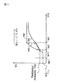
図2に示すように、TAD135により、ノード142の電圧レベルは、時刻ta3にΔV1の電圧値だけさらに低下する。TAD135のアシストがない時、ノード142の電圧変動は、波形205で示すようにゆっくりと進む。長く負荷の大きいネットの場合、TAD135のアシストがないと、ノード142の電圧変動の進捗速度はさらに低下する。
【0026】
信号102がネット110を伝わるとき、他のTAD(例えばTAD140)は、ネット110上の他のノードの電圧が論理レベル『0』へ変化し易くする。これによって、信号102のネット110における伝送速度はさらに上がる。
従来の手法では、中継器(インバータ)を使用してネットにおける信号の伝送速度を上げていた。しかし、中継器を奇数個設けることによって、伝送信号の極性(電圧変動)が反転する。本発明によれば、優位にも、ネットにおける信号の伝送速度を上げるために中継器を使用することを回避できる。加えて、本発明に係るTADは、伝送信号の極性を反転させない。
【0027】
本発明のプリチャージ法によれば、近接ネットは、評価期間の前に、特定の電圧レベル(例えば論理レベル『1』)までプリチャージされる。このプリチャージ法によって、従来の方法の「近接効果」問題を回避できる。ちなみに、近接効果は、近接ネットを伝わる信号が逆方向へ切り替えられたときに生じる。近接効果の問題は、有効切り替え静電容量の増加を引き起し、信号の伝送遅延時間の増加を招く。本発明のプリチャージ法では、近接ネットを伝わる信号は、逆方向へ切り替わらない。1つのネット上の信号が1つの方向に切り替わると、近接ネット上の他の信号は、同一方向に切り替わるか、或いは、現在の極性を維持する。
【0028】
図3、図4および図5は、本発明の機能性について示すものである。図3は、本発明の第2実施例に係る信号伝送システム300の概略ブロック図である。システム300は、信号305を受信するためのレシーバ112、325および330を備えている。TAD135、140、345および350は、ノードB2、B3、B4およびB5でネット110に接続される。TAD135、140、345および350は、それぞれ対応するノードの電圧レベルが閾値(例えば、VDD−Vthreshold 、ここで、Vthreshold は、例えば、およそ0.25ボルトに等しい)に達すると、そのノードの電圧レベルを変化させる。図4は、ネット410で信号405を送信する従来の信号伝送システム400を示す。ドライバ415は、レシーバ420、425および430によって受信される信号405を駆動する。信号405は、ネット410上のノードB1T〜B5Tを介して伝わり、その後レシーバ420によって受信される。
【0029】
図5は、ネット110上のノードB1〜B5における電圧レベルとネット410上のノードB1T〜B5Tにおける電圧レベルとを特定の時間に関連づけて比較するためのグラフを示す。TAD135、140、345および350は、ノードB2、B3、B4およびB5の電圧が論理レベル『1』から論理レベル『0』へと変化し易くする。これによって、論理レベル『1』から論理レベル『0』への電圧変動は、ノードB2T〜B5TでのものよりもノードB2〜B5での方が速くなる。例えば、ノードB5の電圧レベルは、評価期間(図5参照)の開始からおよそ1.2ナノ秒後に論理レベル『0』(0.0ボルト)まで低下する。一方、ノードB5Tの電圧レベルは、評価期間の開始からおよそ2.2ナノ秒後に最低電圧レベルの200ミリボルトまで低下する。評価期間 (evaluation period)は、図5に示すように、プリチャージクロック信号が論理レベル『1』へと立ち上がると同時に開始する。ノードB2〜B5における電圧変動の方が進捗速度が高いのは、TAD135、140、345および350によってアシストされるからである。ノードB2〜B5における電圧変動の方が進捗速度が高いことによって、ネット110における信号305の伝送速度が上がる。
【0030】
図6は、本発明の第3実施例に係る信号伝送システム500の概略ブロック図である。信号伝送システム500は、高い切り替え速度と優れたノイズ不活性との一方を犠牲にして他方を実現することできるプログラマブルTAD (programmable TAD) 505を備えている。プログラマブルTAD505は、ノード142でネット110に接続される。TAD505のプログラマブル機能 (programmable features)は、TADの回路構成にNチャネル型トランジスタ510を加えるか否かによって異なる。具体的には、Nチャネル型トランジスタ510は、ドレインがノード157に接続され、ソースがVSSに接続される。Nチャネル型トランジスタ510のゲートは、二頭の矢印515で示すように、ノード142に接続されるか、或いは、VSSに接続される。TAD505を備えた集積回路チップ(図示しない)の最終金属層(final metal layer:図示しない)を改造することによって、Nチャネル型トランジスタ510のゲートをノード152かVSSかに接続させる。
[例1:Nチャネル型トランジスタ510のゲートをVSSに接続した場合]
Nチャネル型トランジスタ510のゲートがVSSに接続されると、Nチャネル型トランジスタ510は、TAD505の回路構成から切り離される。従って、TAD505は、図1のTAD135と同様に機能し、ノード142の電圧を論理レベル『1』から論理レベル『0』へと変化させるための高速切り替えを行うことができるようになる。ここで、VDDがおよそ1.8ボルトに等しく、Pチャネル型トランジスタ155の閾値電圧(Vthreshold(transistor 155) )がおよそ0.25ボルトであるとすると、Pチャネル型トランジスタ155のゲート(或いは、ノード142)の電圧レベルは、VDD−Vthreshold(transistor 155) =1.8ボルト−0.25ボルト=1.55ボルトまで低下する。そして、Pチャネル型トランジスタ155はオンになる。Pチャネル型トランジスタ150および155がオンになり、Nチャネル型トランジスタ160はオフのままなので、ノード157の電圧は、VSSレベルからVDDレベルへと変化する。Nチャネル型トランジスタ170は、ノード157からVDD電圧レベルを受け取るのでオンになる。Nチャネル型トランジスタ170がオンになるので、ノード142はVSS(論理レベル『0』)へ変化する。このように、Nチャネル型トランジスタ510のゲートがVSSに接続されると、TAD505は、切り替えを開始し、ノード142の電圧レベルが閾値、例えば、1.55ボルトまで低下するのに応え、そのノード142を論理レベル『0』へ変化させる。
[例2:Nチャネル型トランジスタ510のゲートをノード142に接続した場合]
Nチャネル型トランジスタ510のゲートがノード142に接続されると、トランジスタ155および510は、インバータ525を構成する。インバータ525は、入力端子がノード142に接続され、出力端子がノード157に接続される。インバータ525の切り替え電圧VSWは、典型的に、およそ(2/3)VDD=1.2ボルトに維持される。従って、ノード142の電圧がおよそ(2/3)VDD=1.2ボルトにまで低下すると、インバータ525は、ノード157を論理レベル『1』の電圧レベルへと切り替える。ノード157が高レベルに切り替えられるので、トランジスタ170はオンになる。従って、ノード142はVSSへ変化し、ノード142での論理レベル『1』から論理レベル『0』への電圧変動は完了する。
【0031】
トランジスタ510のゲートをノード142に接続することによって、TAD505によりノード142を論理レベル『0』へと変化させ易くなる前は、ノード142では比較的低い電圧レベルのおよそ0.9ボルトが必要とされる。従って、TAD505は、ノイズに対して優れた不活性を示す。TAD505は、高ノイズ度或いは高干渉度を示す環境において特に有用である。ノイズに対する優れた不活性を得るために犠牲にされた結果として、TAD505の切り替え速度は比較的遅い。TAD505によってノード142の電圧を低下させ易くなる前は、ノード142の電圧を比較的低い電圧レベルへ低下させる必要があるからである。
【0032】
図7は、本発明の第4実施例に係る信号伝送システム600の一部を示す図である。信号伝送システム600は、ノード142でネット110に接続されたプログラマブルTAD605を備えている。TAD605のプログラマブル性は、TAD回路構成にNチャネル型トランジスタ(Nチャネル型トランジスタ610など)を追加して、TAD605のノイズに対する不活性をさらに向上させることによって達成される。Nチャネル型トランジスタ610は、ゲートがノード142に接続され、ドレインがノード157に接続され、そして、ソースがVSSに接続される。Pチャネル型トランジスタ155と並列Nチャネル型トランジスタ対510および610とでインバータ620が構成される。インバータ620は、入力端子がノード142に接続され出力端子がノード157に接続される。並列Nチャネル型トランジスタ対510および610は、インバータ620内の大規模トランジスタ (large size transistor)を効果的に構成する。これによって、インバータ620の切り替え電圧VSWは、(2/3)VDD未満まで低下する。このように、インバータ620がノード157を論理レベル『1』へ切り替えてトランジスタ170をオンにする前は、ノード142の電圧を(2/3)VDD未満まで低下させなければならない。Nチャネル型トランジスタ170がオンになると、ノード142はVSS(論理レベル『0』)へ変化する。
【0033】
Nチャネル型トランジスタ610と同様に、さらなるNチャネル型トランジスタをTAD605の回路構成に追加してもよい。このように、Nチャネル型トランジスタをさらに追加することで、インバータ620の切り替え電圧VSWの値が、典型的には、およそ(2/3)VDDからおよそ(1/2)VDDまでの範囲でさらに低下するので、TAD605のノイズ不活性がさらに向上する。
【0034】
図8は、本発明の第5実施例に係る信号伝送システム700であって、システムの電力投入中および/またはシステムリセット中にネット705を論理レベル『0』までプリチャージするという信号伝送システムの概略ブロック図である。TAD710は、ノード712を介してネット705に接続され、インバータ715で構成される。インバータ715は、出力端子がPチャネル型トランジスタ720およびNチャネル型トランジスタ725のゲートに接続される。インバータ715の入力端子は、インバータ716の出力端子に接続される。インバータ716は、入力端子を介してプリチャージクロック信号CLKを受け取る。
【0035】
Pチャネル型トランジスタ720は、ソースがVDDに接続され、ドレインがノード730に接続される。Nチャネル型トランジスタ732は、ドレインがノード730に接続され、ソースがNチャネル型トランジスタ725のドレインに接続され、そして、ゲートがノード712に接続される。Nチャネル型トランジスタ725は、ソースがVSSに接続される。
【0036】
Pチャネル型トランジスタ735は、ソースがVDDに接続され、ドレインがノード712に接続され、そして、ゲートがノード730に接続される。Nチャネル型トランジスタ737は、ドレインがネット705に接続され、ソースがVSSに接続され、そして、ゲートがインバータ716の出力端子に接続される。
図8および図9を参照して、TAD710の作用について考察する。図9では、波形750は、TAD710のアシストがある場合のノード712における電圧変動を時間に関連づけて示す。波形755は、TAD710のアシストがない場合のノード712における電圧変動を時間に関連づけて示す。時刻tb0において、ネット705およびノード712は、論理レベル『0』までプリチャージされる。ネット705が、論理レベル『0』までプリチャージされているとき、プリチャージクロック信号CLKは論理レベル『0』の値を示す。低レベルクロック信号CLKは、インバータ716によって論理レベル『1』の信号へと反転させられる。インバータ716からの論理レベル『1』の出力信号で、Nチャネル型トランジスタ737はオンになる。Nチャネル型トランジスタ737は、プリチャージ中で評価期間の前にネット705の電圧レベルをVSS(論理レベル『0』)へ変化させる。
【0037】
ネット705のプリチャージ中、インバータ715は、インバータ716の高レベル出力信号を論理レベル『0』の信号へと反転させる。インバータ715の低レベル出力信号は、Pチャネル型トランジスタ720およびNチャネル型トランジスタ725のゲートへ印加される。Pチャネル型トランジスタ720およびNチャネル型トランジスタ725はオフになる。Nチャネル型トランジスタ732は、ゲートが、プリチャージされて低レベルになっているノード712に接続されているので、Nチャネル型トランジスタ732もオフである。Pチャネル型トランジスタ720はオンなので、ネット705のプリチャージ中であって評価の前にノード730をVDDレベルへ変化させる。
【0038】
ユーザは、次に、従来の外部の制御回路(図示しない)を使用して評価期間を開始させる。制御回路は、プリチャージクロック信号CLKを論理レベル『0』から論理レベル『1』へと切り替える。評価期間の開始中にプリチャージクロック信号CLKが論理レベル『1』に切り替わると、インバータ716の出力は論理レベル『0』の信号になる。インバータ716の低レベル出力信号でNチャネル型トランジスタ737はオフになる。また、インバータ716の低レベル出力信号は、インバータ715によって論理レベル『1』の信号へと反転させられる。インバータ715の高レベル出力信号でPチャネル型トランジスタ720はオフになり、Nチャネル型トランジスタ725はオンになる。このとき、ノード730はVDDレベルを維持する。
【0039】
時刻tb0後、三状態ドライバ (tri-state driver) 745は、論理レベル『1』への電圧変動を伴う信号740を発生させる。時刻tb1で、ノード712の電圧レベルは、Nチャネル型トランジスタ732の閾値電圧(すなわち、Vthreshold(transistor 732) )まで上昇する。これによって、Nチャネル型トランジスタ732がオンになる。Vthreshold(transistor 732) の値は、典型的に、およそ0.25ボルトである。トランジスタ725と732とはオンでトランジスタ720はオフなので、トランジスタ725および732は、ノード730をVDD電圧レベルからVSS接地電圧レベルへと変化させる。ノード730が低レベルになったので、Pチャネル型トランジスタ735は、ゲートを介してノード730のVSS接地電圧値を受け取り、時刻tb2でオンになる。時刻tb3において、Pチャネル型トランジスタ735は、ノード712をVDD(論理レベル『1』)へと変化させる。これで、ノード712における論理レベル『0』から論理レベル『1』への電圧変動が完了する。
【0040】
図9に示すように、TAD710は、ノード712における電圧変動の進捗速度を上げる。例えば、時刻tb3で、波形750は、波形755より電圧値がΔV2だけ高い。
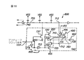
図10は、本発明の第6実施例に係る信号伝送システム800であって、システムの電力投入中および/またはシステムリセット中にネット705を論理レベル『0』までプリチャージするという信号伝送システムの概略ブロック図である。信号伝送システム800は、プログラマブルTAD805を備えている。プログラマブルTAD805は、ノード712を介してネット705に接続される。TAD805は、Pチャネル型トランジスタ770を備えている。Pチャネル型トランジスタ770は、ソースがVDDに接続され、ドレインがノード730に接続される。また、Pチャネル型トランジスタ770のゲートは、二頭の矢印775で示すように、ノード712かVSSかのどちらかに接続可能である。
【0041】
Pチャネル型トランジスタ770のゲートがVSSに接続された場合、トランジスタ770は、TAD805の回路構成から省かれる。TAD805は、図8のTAD710と同様に作用する。特に、前述したように、TAD805により、ノード712の電圧レベルがトランジスタ732の閾値電圧Vthreshold(transistor 732) まで上昇するのに応えてノード712をVDDへと変化させ易くなる。なお、Vthreshold(transistor 732) は、典型的に、およそ0.25ボルトである。
【0042】
Pチャネル型トランジスタ770のゲートがノード712に接続されると、トランジスタ770および732によりインバータ780が構成される。インバータ780は、入力端子がノード712に接続され、出力端子がノード730に接続され、そして、Pチャネル型トランジスタ735のゲートを駆動する。VDDがおよそ1.8ボルトに等しいとすると、ノード712の電圧がVSW=VDD/3=1.8/3=0.6ボルトまで上昇したとき、インバータ780は、ノード730の電圧レベルを論理レベル『1』から論理レベル『0』へと切り替える。しかしながら、Pチャネル型トランジスタ(図示しない)を追加してPチャネル型トランジスタ770に並列に接続することによって、インバータ780の切り替え電圧VSWを別の値(典型的には、(1/3)VDDから(1/2)VDDの範囲)へと調節してもよい。
【0043】
ノード730における論理レベル『0』の電圧でPチャネル型トランジスタ735はオンになる。Pチャネル型トランジスタ735は、ノード712をVDD(論理レベル『1』)へ変化させる。ノード712における論理レベル『0』から論理レベル『1』への電圧変動は、これで完了する。
TAD805は、ノード712の電圧を例えばVDD/3へと上昇するまでノード712を論理レベル『1』まで変化させ易くなるようにアシストしないので、ノイズに対して優れた不活性を示す。優れたノイズ不活性のために犠牲にされた結果、TAD805の切り替え速度は低い。
【0044】
図示しない別の実施例では、Pチャネル型トランジスタ770と同様に、別のPチャネル型トランジスタ(図示しない)をTAD805の回路構成に加える。このように、Pチャネル型トランジスタを加えることによって、インバータ780の切り替え電圧VSWが上昇し、TADのノイズ不活性が一層優れたものとなる。
【0045】
図11は、本発明の第7実施例に係る信号伝送システム900であって、双方向性の信号伝送機能を備えたシステム900の概略ブロック図である。例えば、ドライバ905は、信号を915方向へネット910を介して駆動し、ドライバ920は、信号を925方向へネット910を介して駆動する。別のドライバ(ドライバ930と935など)を追加してネット910に接続し、ネット910を介して信号を駆動させるようにしてもよい。
【0046】
TAD940および/または945は、ネット910に接続されネット910おける信号の伝送速度を上昇させ易くする。具体的に、TAD940および945は、ノード947と949でネット910に接続される。ネット910に接続されるTADの個数は様々に異なる。ノードの電圧レベルが、ネット910を伝わる信号によって上昇して閾値に達すると、TAD940および945は、それぞれ対応するノードにおける電圧レベルを変化させる。システムの電力投入中および/またはシステムリセット中にネット910がロウ論理レベルまでプリチャージされた場合、TAD940および945は、対応するノードにおける電圧レベルを論理レベル『1』へと変化させる。TAD940と945は、それぞれ前述した様々なTADの実施例に適用される。
【0047】
TAD940および945は、それぞれ915方向に伝送する信号の伝送速度を上昇させるか、或いは、反対方向925に伝送する別の信号の伝送速度を上昇させる。このため、TADのアシストを受けて高速で信号を送信するために、ネット910上の様々な位置にドライバを設置することができる。
図12は、双方向性の信号伝送機能を備えた従来のシステム950を示す。従来のシステム950は、ドライバ955、960および965を備えている。ドライバ955、960および965は、様々に異なるノードでネット970に接続される。ドライバ955は、975方向へネット970を介して信号を送信できるものとする。従来のシステム950では、ドライバ955が信号を送信する場合、中継器980および985をオフにすることが必要である。中継器980および985をオフにすることによって、975方向の信号は中継器990と995を渡って伝送する。また、ドライバ965が、997方向にネット970を介して信号を送信する場合、中継器990および995をオフにしなければならない。こうすれば、997方向の信号は、中継器980および985を渡って伝送できる。このように、従来の方法によれば、ネットを伝送する信号の方向に基づいてネット上の中継器を調節することが必要である。一方、本発明によれば、信号方向の相違に従って信号伝送システムを調節する必要もなく、信号の915方向或いは925方向(図11)への伝送速度を自動的に上昇させることができる。
【0048】
本発明の様々な実施例によれば、集積回路内に形成されるネットにおける信号の伝送速度を上昇させられる。例えば、先に考察したTADの様々な実施例は、レジスタファイル内のワード線或いは追加命令バッファ (re-order buffer)内のワード線に接続される。ワード線とは、比較的短い導体であって、単一のドライバによって駆動され、信号の伝送遅延時間を増加させる大きな容量性負荷を伴う。
【0049】
先に考察したTADの様々な実施例は、マイクロプロセッサのリザルトバス (result bus) に接続される。リザルトバスは、多数のドライバによって駆動され、その結果、双方向の信号伝送機能を発揮する。
先に考察したTADの様々な実施例は、追加命令バッファ内のビット線に接続することもできる。ビット線は、多数のドライバによって駆動され、その結果、双方向の信号伝送機能を発揮する。ビット線は、比較的短い導体であって、信号の伝送遅延時間を増加させる大きな容量性負荷を伴う。
【0050】
付記 本発明は以下の特徴を有する。
(付記1) 集積回路内に存在する第1のノードを含むネットを介して信号を送信するための装置であって、
前記ネットに接続され、該ネットを介して前記信号を駆動するドライバと、
前記ネットにおける前記第1のノードに接続され、該第1のノードの電圧レベルが閾値に到達するのに応えて当該第1のノードの電圧レベルを変化させる第1の状態変化アシストドライバ(TAD)と、を備えることを特徴とする装置。(請求項1)
【0051】
(付記2) 付記1に記載の装置において、前記ネットが論理レベル『1』にプリチャージされているとき、前記第1のTADは、前記第1のノードを論理レベル『0』へ変化させることを特徴とする装置。
(付記3) 付記1に記載の装置において、前記ネットが論理レベル『0』にプリチャージされているとき、前記第1のTADは、前記第1のノードを論理レベル『1』へ変化させることを特徴とする装置。
【0052】
(付記4) 付記1に記載の装置において、前記第1のTADは、前記第1のノードを論理レベル『0』へ変化させ、そして、該第1のTADは、
前記第1のノードに接続された第1の端子、接地された第2の端子、および、ゲート端子を有する第1のトランジスタと、
第1の電源電圧源に接続された第1の端子、第2の端子、および、プリチャージクロック信号の反転信号を受け取るゲート端子を有する第2のトランジスタと、
該第2のトランジスタの第2の端子に接続された第1の端子、前記第1のトランジスタのゲート端子に接続された第2の端子、および、前記第1のノードに接続されたゲート端子を有する第3のトランジスタと、
該第3のトランジスタの第2の端子に接続された第1の端子、接地された第2の端子、および、前記プリチャージクロック信号の反転信号を受け取るゲート端子を有する第4のトランジスタと、を備えることを特徴とする装置。(請求項2)
【0053】
(付記5) 付記4に記載の装置において、前記第1のTADは、さらに、
前記第1のトランジスタのゲート端子に接続された第1の端子、接地された第2の端子、および、前記第1のノードに接続されるか或いは接地されたゲート端子を有する第5のトランジスタを備えることを特徴とする装置。
(付記6) 付記4に記載の装置において、前記第1のTADは、さらに、
前記第1のトランジスタのゲート端子に接続された第1の端子、接地された第2の端子、および、前記第1のノードに接続されたゲート端子を有する第6のトランジスタを備えることを特徴とする装置。
【0054】
(付記7) 付記4に記載の装置において、前記第1のTADは、さらに、
前記ネットを論理レベル『1』にプリチャージするプリチャージトランジスタを備え、該プリチャージトランジスタは、前記第1の電源電圧源に接続された第1の端子、前記ネットに接続された第2の端子、前記プリチャージクロック信号を受け取るゲート端子を有することを特徴とする装置。
【0055】
(付記8) 付記1に記載の装置において、前記第1のTADは、前記第1のノードを論理レベル『1』へ変化させ、そして、該第1のTADは、
第1の電源電圧源に接続された第1の端子、第2の端子、および、プリチャージクロック信号を受け取るゲート端子を有する第1のプルアップトランジスタと、
該第1のプルアップトランジスタの第2の端子に接続された第1の端子、第2の端子、および、前記第1のノードに接続されたゲート端子を有する第1のプルダウントランジスタと、
該第1のプルダウントランジスタの第2の端子に接続された第1の端子、接地された第2の端子、および、前記プリチャージクロック信号を受け取るゲート端子を有する第2のプルダウントランジスタと、
前記第1の電源電圧源に接続された第1の端子、前記第1のノードに接続された第2の端子、および、前記第1のプルアップトランジスタの第2の端子に接続されたゲート端子を有する第2のプルアップトランジスタと、を備えることを特徴とする装置。(請求項3)
【0056】
(付記9) 付記8に記載の装置において、前記第1のTADは、さらに、
前記第1の電源電圧源に接続された第1の端子、前記第1のプルアップトランジスタの第2の端子に接続された第2の端子、および、前記第1のノードに接続されるか或いは接地されたゲート端子を有する第3のプルアップトランジスタを備えることを特徴とする装置。
(付記10) 付記8に記載の装置において、前記第1のTADは、さらに、
前記電源電圧源に接続された第1の端子、前記第1のプルアップトランジスタの第2の端子に接続された第2の端子、および、前記第1のノードに接続されたゲート端子を有する第4のプルアップトランジスタを備えることを特徴とする装置。
【0057】
(付記11) 付記8に記載の装置において、前記第1のTADは、さらに、
前記ネットを論理レベル『0』にプリチャージするプリチャージトランジスタを備え、該プリチャージトランジスタは、前記ネットに接続された第1の端子、接地された第2の端子、および、前記プリチャージクロック信号の反転信号を受け取るゲート端子を有することを特徴とする装置。
(付記12) 付記1に記載の装置において、該装置は、さらに、
さらなる信号を送信して前記ネットにおける双方向信号伝達を可能にする第2のドライバを備えることを特徴とする装置。
(付記13) 付記1に記載の装置において、該装置は、さらに、
第2のノードで前記ネットに接続され、該第2のノードの電圧レベルが閾値に到達するのに応えて当該第2のノードの電圧レベルを変化させる第2のTADを備えることを特徴とする装置。
【0058】
(付記14) 集積回路内において高速の信号伝送を行う装置であって、
第1のノードを有し、前記集積回路内で信号を送信するネットと、
前記第1のノードに接続され、該第1のノードの電圧レベルが閾値に到達するのに応えて当該第1のノードの電圧レベルを変化させる第1の状態変化アシストドライバ(TAD)と、を備えることを特徴とする装置。(請求項4)
(付記15) 付記14に記載の装置において、前記ネットが論理レベル『1』にプリチャージされているとき、前記第1のTADは、前記第1のノードを論理レベル『0』へ変化させることを特徴とする装置。
(付記16) 付記14に記載の装置において、前記ネットが論理レベル『0』にプリチャージされているとき、前記第1のTADは、前記第1のノードを論理レベル『1』へ変化させることを特徴とする装置。
【0059】
(付記17) 第1のノードを含むネットを有する信号伝送システムを使用して集積回路内において高速の信号伝送を行う方法であって、
(a)前記第1のノードの電圧レベルを検知するステップと、
(b)前記第1のノードの電圧が閾値に到達するのに応えて、該第1のノードの電圧レベルを変化させるステップと、を備えることを特徴とする方法。(請求項5)
(付記18) 集積回路内における第1のノードを含むネットを介して高速伝送を達成するための方法であって、
(a)前記ネットにおける第1のノードを介して信号を駆動するステップと、(b)前記信号が前記第1のノードに接近するのにつれて該第1のノードの電圧レベルが閾値に到達するとき、当該第1のノードの電圧レベルを変化させるステップと、を備えることを特徴とする方法。(請求項6)
【0060】
(付記19) 第1のノードを含むネットの電圧レベルを変化させるドライバであって、
前記第1のノードに接続された入力端子、第1の電圧源に接続された第1の端子、第2の電圧源に接続された第2の端子、および、出力端子を有し、前記第1のノードの電圧レベルが閾値になるのに応えてオンになるように構成された第1の変化回路と、
該第1の変化回路の出力端子に接続された入力端子、前記第1のノードに接続された第1の端子、および、前記第2の電圧源に接続された第2の端子を有し、前記第1の変化回路がオンになるのに応えて前記第1のノードを前記第2の電圧源の電位へ変化させる第2の変化回路と、を備えることを特徴とするドライバ。
【0061】
(付記20) 第1のノードを含むネットの電圧レベルを変化させるドライバであって、
前記第1のノードに接続された入力端子、第1の電圧源に接続された第1の端子、第2の電圧源に接続された第2の端子、および、出力端子を有し、前記第1のノードの電圧レベルが閾値になるのに応えてオンになるように構成された第1の変化回路と、
該第1の変化回路の出力端子に接続された入力端子、前記第1の電圧源に接続された第1の端子、および、前記第1のノードに接続された第2の端子を有し、前記第1の変化回路がオンになるのに応えて前記第1のノードを前記第1の電圧源の電位へ変化させる第2の変化回路と、を備えることを特徴とするドライバ。
【0062】
(付記21) 付記14に記載の装置において、前記第1のTADは、前記ネットを介して第1の方向に伝送される信号の伝送速度を増加することを特徴とする装置。
(付記22) 付記14に記載の装置において、前記第1のTADは、前記ネットを介して第2の方向に伝送される信号の伝送速度を増加することを特徴とする装置。
【0063】
(付記23) 付記14に記載の装置において、前記第1のTADは、前記第1のノードを論理レベル『0』へ変化させ、そして、該第1のTADは、
前記第1のノードに接続された第1の端子、接地された第2の端子、および、ゲート端子を有する第1のトランジスタと、
第1の電源電圧源に接続された第1の端子、第2の端子、および、プリチャージクロック信号の反転信号を受け取るゲート端子を有する第2のトランジスタと、
前記第2のトランジスタの第2の端子に接続された第1の端子、前記第1のトランジスタのゲート端子に接続された第2の端子、および、前記第1のノードに接続されたゲート端子を有する第3のトランジスタと、
前記第3のトランジスタの第2の端子に接続された第1の端子、接地された第2の端子、および、前記プリチャージクロック信号の反転信号を受け取るゲート端子を有する第4のトランジスタと、を備えることを特徴とする装置。
【0064】
(付記24) 付記23に記載の装置において、前記第1のTADは、さらに、前記第1のトランジスタのゲート端子に接続された第1の端子、接地された第2の端子、および、前記第1のノードに接続されるか或いは接地されたゲート端子を備えた第5のトランジスタを備えることを特徴とする装置。
(付記25) 付記23に記載の装置において、前記第1のTADは、さらに、前記第1のトランジスタのゲート端子に接続された第1の端子、接地された第2の端子、および、前記第1のノードに接続されたゲート端子を有する第6のトランジスタを備えることを特徴とする装置。
(付記26) 付記23に記載の装置において、前記第1のTADは、さらに、前記ネットを論理レベル『1』にプリチャージするプリチャージトランジスタを備え、該プリチャージトランジスタは、前記第1の電源電圧源に接続された第1の端子、前記ネットに接続された第2の端子、前記プリチャージクロック信号を受け取るゲート端子を有することを特徴とする装置。
【0065】
(付記27) 付記14に記載の装置において、前記第1のTADは、前記第1のノードを論理レベル『1』へ変化させ、そして、該第1のTADは、
第1の電源電圧源に接続された第1の端子、第2の端子、および、プリチャージクロック信号を受け取るゲート端子を有する第1のプルアップトランジスタと、
該第1のプルアップトランジスタの第2の端子に接続された第1の端子、第2の端子、および、前記第1のノードに接続されたゲート端子を有する第1のプルダウントランジスタと、
該第1のプルダウントランジスタの第2の端子に接続された第1の端子、接地された第2の端子、および、前記プリチャージクロック信号を受け取るゲート端子を有する第2のプルダウントランジスタと、
前記第1の電源電圧源に接続された第1の端子、前記第1のノードに接続された第2の端子、および、前記第1のプルアップトランジスタの第2の端子に接続されたゲート端子を有する第2のプルアップトランジスタと、を備えることを特徴とする装置。
【0066】
(付記28) 付記27に記載の装置において、前記第1のTADは、さらに、前記第1の電源電圧源に接続された第1の端子、前記第1のプルアップトランジスタの第2の端子に接続された第2の端子、および、前記第1のノードに接続されるか或いは接地されたゲート端子を有する第3のプルアップトランジスタを備えることを特徴とする装置。
(付記29) 付記27に記載の装置において、前記第1のTADは、さらに、前記電源電圧源に接続された第1の端子、前記第1のプルアップトランジスタの第2の端子に接続された第2の端子、および、前記第1のノードに接続されたゲート端子を有する第4のプルアップトランジスタを備えることを特徴とする装置。
【0067】
(付記30) 付記27に記載の装置において、前記第1のTADは、さらに、前記ネットを論理レベル『0』にプリチャージするプリチャージトランジスタを備え、該プリチャージトランジスタは、前記ネットに接続された第1の端子、接地された第2の端子、および、前記プリチャージクロック信号の反転信号を受け取るゲート端子を有することを特徴とする装置。
(付記31) 付記14に記載の装置において、該装置は、さらに、
第2のノードで前記ネットに接続され、該第2のノードの電圧レベルが閾値に到達するのに応えて当該第2のノードの電圧レベルを変化させる第2のTADを備えることを特徴とする装置。
【0068】
(付記32) 付記17に記載の方法において、前記ネットが論理レベル『1』にプリチャージされているとき、前記変化させるステップ(b)において、前記第1のノードの電圧レベルを論理レベル『0』へ変化させることを特徴とする方法。
(付記33) 付記17に記載の方法において、前記ネットが論理レベル『0』にプリチャージされているとき、前記変化させるステップ(b)において、前記第1のノードの電圧レベルを論理レベル『1』へ変化させることを特徴とする方法。
(付記34) 付記17に記載の方法において、前記変化させるステップ(b)は、
該ステップ(b)の閾値を、より高速のスイッチング速度と前記信号伝送システムのノイズ不活性との折り合いを付ける特定のレベルに設定することを備えることを特徴とする方法。
【0069】
(付記35) 付記17に記載の方法において、前記変化させるステップ(b)は、
第1の信号が前記ネットを介して第1の方向に伝わるとき、前記第1のノードの電圧レベルを変化させることを備えることを特徴とする方法。
(付記36) 付記17に記載の方法において、前記変化させるステップ(b)は、
第2の信号が前記ネットを介して第2の方向に伝わるとき、該第1のノードの電圧レベルを変化させることを備えることを特徴とする方法。
(付記37) 付記17に記載の方法において、該方法は、さらに、
第2のノードの電圧レベルが閾値に到達するのに応えて、該ネットにおける第2のノードの電圧レベルを変化させるステップを備えることを特徴とする方法。
【0070】
(付記38) 付記17に記載の方法において、該方法は、さらに、
隣接するネット間の信号を逆にスイッチングするのを回避するために、前記集積回路における少なくとも2つの隣接するネットの電圧レベルをプリチャージするステップを備えることを特徴とする方法。
(付記39) 付記18に記載の方法において、該方法は、さらに、
前記集積回路のノイズ不活性を調整するために、前記ステップ(b)の閾値を設定するステップを備えることを特徴とする方法。
【0071】
(付記40) 付記18に記載の方法において、該方法は、さらに、
第2のノードを介して前記電圧レベルが閾値に到達して前記信号が該第2のノードに接近するとき、前記ネットにおける第2のノードの電圧レベルをプリチャージするステップを備えることを特徴とする方法。
(付記41) 付記18に記載の方法において、該方法は、さらに、
隣接するネット間の信号を逆にスイッチングするのを回避するために、前記集積回路における少なくとも2つの隣接するネットの電圧レベルをプリチャージするステップを備えることを特徴とする方法。
【0072】
(付記42) 集積回路内において第1のノードを含むネットを介して信号の高速伝送を行う装置であって、
前記ネットに接続され、該ネットを介して前記信号を駆動する手段と、
前記ネットに接続され、前記第1のノードの電圧レベルが閾値に到達するのに応えて当該第1のノードの電圧レベルを変化させる第1の手段と、を備えることを特徴とする装置。
(付記43) 付記42に記載の装置において、該装置は、さらに、
前記ネットに接続され、前記第2のノードの電圧レベルが閾値に到達するのに応えて当該第2のノードの電圧レベルを変化させる第2の手段を備えることを特徴とする装置。
(付記44) 付記19に記載のドライバにおいて、前記第2の変化回路は、
前記第1のノードに接続された第1の端子、前記第2の電圧源に接続された第2の端子、および、前記第1の変化回路の出力端子に接続されたゲート端子を有する第1のトランジスタを備えることを特徴とするドライバ。
【0073】
(付記45) 付記19に記載のドライバにおいて、前記第1の変化回路は、
前記第1の電圧源に接続された第1の端子、第2の端子、および、反転されたクロック信号を受け取るゲート端子を有する第2のトランジスタと、
該第2のトランジスタの第2の端子に接続された第1の端子、前記第2の変化回路の入力端子に接続された第2の端子、および、前記第1のノードに接続されたゲート端子を有する第3のトランジスタと、
該第3のトランジスタの第2の端子に接続された第1の端子、前記第2の電圧源に接続された第2の端子、および、前記反転されたクロック信号を受け取るゲート端子を有する第4のトランジスタと、を備えることを特徴とするドライバ。
【0074】
(付記46) 付記19に記載のドライバにおいて、該ドライバは、さらに、
前記第1の電圧源に接続された第1の端子、前記ネットに接続された第2の端子、および、クロック信号を受け取るゲート端子を有するプリチャージトランジスタを備えることを特徴とするドライバ。
(付記47) 付記19に記載のドライバにおいて、該ドライバは、さらに、
前記第2の変化回路の入力端子に接続された第1の端子、前記第2の電圧源に接続された第2の端子、および、前記第1のノード或いは前記第2の電圧源に接続されたゲート端子を有する第5のトランジスタを備えることを特徴とするドライバ。
(付記48) 付記20に記載のドライバにおいて、前記第2の変化回路は、
前記第1の電圧源に接続された第1の端子、前記第1のノードに接続された第2の端子、および、前記第1の変化回路の出力端子に接続されたゲート端子を有する第1のトランジスタを備えることを特徴とするドライバ。
【0075】
(付記49) 付記20に記載のドライバにおいて、前記第1の変化回路は、
前記第1の電圧源に接続された第1の端子、第2の端子、および、クロック信号を受け取るゲート端子を有する第2のトランジスタと、
該第2のトランジスタの第2の端子に接続された第1の端子、前記第2の変化回路の入力端子に接続された第2の端子、および、前記第1のノードに接続されたゲート端子を有する第3のトランジスタと、
該第3のトランジスタの第2の端子に接続された第1の端子、前記第2の電圧源に接続された第2の端子、および、前記クロック信号を受け取るゲート端子を有する第4のトランジスタと、を備えることを特徴とするドライバ。
【0076】
(付記50) 付記20に記載のドライバにおいて、該ドライバは、さらに、
前記ネットに接続された第1の端子、前記第2の電圧源に接続された第2の端子、および、クロック信号を受け取るゲート端子を有するプリチャージトランジスタを備えることを特徴とするドライバ。
(付記51) 付記20に記載のドライバにおいて、該ドライバは、さらに、
前記第1の電圧源に接続された第1の端子、前記第2の変化回路の入力端子に接続された第2の端子、および、前記第1のノード或いは前記第2の電圧源に接続されたゲート端子を有する第5のトランジスタを備えることを特徴とするドライバ。
【0077】
【発明の効果】
以上、詳述したように、本発明によれば、近接効果による伝送遅延時間の増加を招くことなく、集積回路内のネット上での信号の伝送速度を上げることができる。
【図面の簡単な説明】
【図1】本発明の第1実施例に係る信号伝送システムであって、状態変化アシストドライバ(TAD)で信号の伝送速度を上げるようにした信号伝送システムを概略的に示すブロック図である。
【図2】図1に示す信号伝送システム内の特定のノードにおける電圧変動を表す第1の波形、および、TADによってアシストされない場合の同一のノードにおける電圧変動を表す第2の波形のグラフを示す図である。
【図3】本発明の第2実施例に係る信号伝送システムであって別のTADが追加された信号伝送システムの概略ブロック図である。
【図4】従来の信号伝送システムを概略的に示すブロック図である。
【図5】図3および図4の信号伝送システム内の異なるノードにおける電圧レベルを表す様々な波形のグラフを示す図である。
【図6】本発明の第3実施例に係る信号伝送システムであって、高い切り替え速度と優れたノイズ不活性との一方を犠牲にして他方を実現できるプログラマブルTADを備えた信号伝送システムを概略的に示すブロック図である。
【図7】本発明の第4実施例に係る信号伝送システムであって、ノイズ不活性を向上させたプログラマブルTADを備えた信号伝送システムの一部を示す図である。
【図8】本発明の第5実施例に係る信号伝送システムであって、システムへの電力投入中および/またはシステムリセット中にプリチャージされて論理レベル『0』になったネットにTADが接続される信号伝送システムを概略的に示すブロック図である。
【図9】図8の信号伝送システム内のノードにおける電圧変動を表す第1の波形、および、TADによってアシストされない場合の同一ノードにおける電圧変動を表す第2の波形のグラフを示す図である。
【図10】本発明の第6実施例に係る信号伝送システムであって、高い切り替え速度と優れたノイズ不活性との一方を犠牲にして他方を実現できるプログラマブルTADを備えた信号伝送システムを概略的に示すブロック図である。
【図11】本発明の第7実施例に係る信号伝送システムであって、多数のドライバをネットに接続してネットにおける双方向信号伝送を可能にした信号伝送システムを概略的に示すブロック図である。
【図12】ネットにおける双方向信号伝送を可能にした従来の信号伝送システムを概略的に示すブロック図である。
【符号の説明】
100,300,400,500,600,700,800,900,950…信号伝送システム
105,115.120,125,415,905,920,930,935,955,960,965…ドライバ
110,410,705…ネット(信号経路)
112,325,330,420,425,430…レシーバ
135,140,345,350,710,940,945…状態変化アシストドライバ(TAD)
505,605,805…プログラマブルTAD
510,610…Nチャネル型トランジスタ
525,620,780…インバータ
745…三状態ドライバ
770…Pチャネル型トランジスタ770
CLK…プリチャージクロック信号[0001]
BACKGROUND OF THE INVENTION
The present invention relates generally to the field of data transmission, and more particularly to an apparatus and method for increasing the transmission rate of a signal in a signal path within an integrated circuit.
[0002]
[Prior art]
The signal transmission delay time increases as the length of the signal path in the network increases. The transmission delay time is relatively long for signals transmitted over “heavy” networks (ie, networks and nets with large capacitive loads). This is because the RC delay time of the transmission signal becomes long when the capacitive load is large. Here, the heavy net is, for example, an SRAM word line.
[0003]
As the size of the configuration decreases, the resistance value in the metal layer within the integrated circuit increases. As the resistance value increases, the RC delay of the signal transmitted over the net formed in the metal layer increases.
The period of the microprocessor becomes longer as the transmission delay time of the signal processed by the microprocessor increases. In addition, if the transmission delay time of signals on the critical net becomes long, the timing requirement in the “critical net (critical path)” may not be satisfied.
[0004]
[Problems to be solved by the invention]
According to the conventional method, a repeater formed by an inverter is usually inserted into a long net to increase the signal transmission speed. A repeater splits a long net into a number of short nets, where each repeater drives one short net. In many cases, the desired signal timing (or optimal timing) is achieved by inserting an odd number of inverters. However, by inserting an odd number of inverters, the polarity of the transmission signal is inverted (the voltage varies). In order to restore the original polarity of the transmission signal, another inverter is added to the net to make the number of inverters an even number. However, the addition of another inverter increases the delay and may result in the desired signal timing constraints (or optimal timing values) for the net not being satisfied.
[0005]
Conventional methods also have a “neighbor effect” problem. Proximity effects occur when a signal transmitted through a nearby net (proximity net) changes direction to the opposite side. The proximity effect causes an increase in effective switching capacitance, resulting in an increase in signal transmission delay time.
Accordingly, there is a need for a method and apparatus that can increase the transmission speed of signals over a net in an integrated circuit and solve the problems in the conventional methods described above.
[0006]
The problem of RC delay is severe, for example, in a net driven by any one of a number of drivers connected to the net. Because repeaters are unidirectional, the driver cannot send signals to all parts of the net, and therefore cannot use repeaters on the net. Such a net is, for example, a result bus of a multi-function unit. A method and apparatus for improving transmission delay in such an embodiment is desired. In the conventional method for solving this, a bidirectional repeater is used. However, bidirectional repeaters are slow and require a control circuit to determine the direction of signal flow. This control circuit not only increases the cost of area, but also causes speed problems due to the control circuit itself.
[0007]
[Means for Solving the Problems]
According to the present invention, a driver is connected to a node included in a net that drives a signal, and an auxiliary driver that assists the driver in driving the signal is connected to a source terminal connected to a power source and to the node. A drain terminal; a first transistor having a gate terminal to which a precharge clock signal is input; a grounded source terminal; a drain terminal connected to the node; a second transistor having a gate terminal; A third terminal having a gate terminal to which an inverted signal of the precharge clock signal is input, a source terminal connected to the drain terminal of the third transistor, A drain terminal connected to the gate terminal of the second transistor and a node connected to the node A fourth transistor having a gate terminal; a grounded source terminal; a drain terminal connected to the drain terminal of the fourth transistor; and a gate terminal to which an inverted signal of the precharge clock signal is input. A fifth transistor; a grounded source terminal; a drain terminal connected to the gate terminal of the second transistor; and a drain terminal of the second transistor. Selectively connected to the child or ground terminal by wiring An auxiliary driver is provided that includes a sixth transistor having a gate terminal.
The present invention provides an apparatus for achieving high speed signal transmission over a net driven by any one of a number of drivers provided in an integrated circuit. This device includes a first driver for driving a signal via a net. A first transition assist driver (TAD) is responsive to the voltage level of the first node reaching a threshold as the signal approaches the first node in response to the first node in the net. Vary the voltage level. When the first node is precharged to the logic level “1”, the first TAD changes the voltage level of the first node to the logic level “0”. When the first node is precharged to the logic level “0”, the first TAD changes the voltage level of the first node to the logic level “1”. When the first TAD changes the voltage level of the first node, the signal transmission speed in the net increases.
[0008]
According to another aspect of the invention, the second TAD is connected to the net at the second node. The second TAD changes the voltage level of the second node as the signal approaches the second node. By changing the voltage level of the second node, the signal transmission speed is further increased. By adding additional TAD and connecting to another node on the net, the transmission rate of the signal on the net may be further increased.
[0009]
According to yet another aspect of the present invention, the above threshold can be adjusted by programming the TAD according to the present invention to increase the switching speed or TAD noise immunity.
In the conventional method, the signal transmission speed in the network is increased by using a repeater (inverter). However, by providing an odd number of repeaters, the polarity of the transmission signal is inverted (the voltage varies). The present invention is advantageous because it avoids the use of repeaters to increase the transmission rate of signals on the net. In addition, the TAD according to the present invention does not invert the polarity of the transmission signal.
[0010]
According to another aspect of the present invention, a precharge method is employed in which adjacent nets (adjacent nets) are precharged and the voltage is kept at a specific voltage level. According to this precharge method, the “proximity effect” problem of the conventional method can be avoided. Here, the proximity effect occurs when a signal transmitted through the proximity net is switched in the opposite direction. The problem of the proximity effect causes an increase in effective switching capacitance, resulting in an increase in signal transmission delay time. According to the precharge method of the present invention, the signal on the adjacent net is not switched in the opposite direction. When a signal on one net switches in one direction, the other signal on the adjacent net switches in the same direction or maintains the current polarity.
[0011]
A second driver may be connected to the net to drive the signal to transmit in a direction opposite to the direction of the signal driven by the first driver. In this case, bidirectional signal transmission is achieved in the signal transmission system according to the present invention. If another driver is added at another point on the net, bidirectional signal transmission on the net becomes possible.
[0012]
The TAD according to the present invention changes the voltage level of the corresponding node on the net regardless of the signal transmission direction on the net. The TAD automatically detects a change in the voltage level of a corresponding node caused by a signal transmitted on the net, and changes the voltage level of the corresponding node to increase the signal transmission speed.
[0013]
DETAILED DESCRIPTION OF THE INVENTION
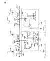
FIG. 1 shows a
[0014]
The resistors and capacitors placed on the net 110 are denoted by R and C. Capacitor C represents the capacitive characteristic and / or capacitive load of
[0015]
The
[0016]
The
[0017]
According to the present invention, the number of TADs connected to the net 110 varies. According to an alternative embodiment not shown, only one TAD is connected to the net 110. Alternatively, another TAD and driver and / or receiver are added to the net 110 in the
By using
[0018]
The operation of the
[0019]
Since the net 110 is precharged and is at a high level, the
During the precharge of the net 110, the
[0020]
The user then starts an evaluation period using a conventional external control circuit (not shown). The control circuit switches the precharge clock signal CLK from the logic level “0” to the logic level “1”. When the precharge clock signal CLK is switched to the logic level “1”, the P-
[0021]
According to an alternative embodiment of the present invention, the precharge clock signal CLK may be generated by an on-chip (internal) clock source (not shown). The on-chip clock source generates a precharge clock signal CLK. The precharge clock signal is applied to the input terminal of
[0022]
After the time ta0 (see FIG. 2), the
[0023]
At time ta1, the voltage of the
[0024]
Since the voltage of the
[0025]
As shown in FIG. 2, the voltage level of the
[0026]
When the
In the conventional method, a repeater (inverter) is used to increase the signal transmission speed on the network. However, the polarity (voltage fluctuation) of the transmission signal is reversed by providing an odd number of repeaters. Advantageous Effects of the Invention According to the present invention, it is possible to avoid the use of a repeater to increase the transmission speed of signals on the network. In addition, the TAD according to the present invention does not invert the polarity of the transmission signal.
[0027]
According to the precharge method of the present invention, the proximity net is precharged to a specific voltage level (eg, logic level “1”) before the evaluation period. By this precharge method, the “proximity effect” problem of the conventional method can be avoided. Incidentally, the proximity effect occurs when a signal transmitted through the proximity net is switched in the reverse direction. The problem of the proximity effect causes an increase in effective switching capacitance, resulting in an increase in signal transmission delay time. In the precharge method of the present invention, the signal transmitted through the proximity net is not switched in the reverse direction. When a signal on one net switches in one direction, the other signals on the neighboring nets switch in the same direction or maintain the current polarity.
[0028]
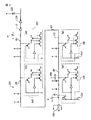
3, 4 and 5 illustrate the functionality of the present invention. FIG. 3 is a schematic block diagram of a signal transmission system 300 according to the second embodiment of the present invention. System 300 includes
[0029]
FIG. 5 shows a graph for comparing the voltage levels at nodes B1 to B5 on net 110 with the voltage levels at nodes B1T to B5T on net 410 in relation to a specific time. The
[0030]
FIG. 6 is a schematic block diagram of a
[Example 1: When the gate of the N-
When the gate of the N-
[Example 2: When the gate of the N-
When the gate of N-
[0031]
By connecting the gate of
[0032]
FIG. 7 is a diagram showing a part of a
[0033]
Similar to the N-
[0034]
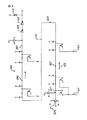
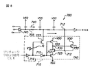
FIG. 8 shows a
[0035]
In the P-
[0036]
In the P-channel transistor 735, the source is connected to VDD, the drain is connected to the
The action of
[0037]
During the precharge of the net 705, the inverter 715 inverts the high level output signal of the
[0038]
The user then starts the evaluation period using a conventional external control circuit (not shown). The control circuit switches the precharge clock signal CLK from the logic level “0” to the logic level “1”. When the precharge clock signal CLK is switched to the logic level “1” during the start of the evaluation period, the output of the
[0039]
After time tb0, a
[0040]
As shown in FIG. 9, the
FIG. 10 shows a
[0041]
When the gate of the P-
[0042]
When the gate of P-
[0043]
The voltage of the logic level “0” at the
Since the
[0044]
In another embodiment (not shown), another P-channel transistor (not shown) is added to the
[0045]
FIG. 11 is a schematic block diagram of a
[0046]
The
[0047]
FIG. 12 shows a
[0048]
According to various embodiments of the present invention, the transmission rate of signals in a net formed in an integrated circuit can be increased. For example, the various embodiments of TAD discussed above are connected to a word line in a register file or a word line in a re-order buffer. A word line is a relatively short conductor, driven by a single driver, with a large capacitive load that increases the signal transmission delay time.
[0049]
The various embodiments of TAD discussed above are connected to the microprocessor result bus. The result bus is driven by a large number of drivers, and as a result, exhibits a bidirectional signal transmission function.
The various embodiments of TAD discussed above can also be connected to bit lines in additional instruction buffers. The bit line is driven by a large number of drivers, and as a result, exhibits a bidirectional signal transmission function. A bit line is a relatively short conductor with a large capacitive load that increases the signal transmission delay time.
[0050]
Additional Notes The present invention has the following features.
(Appendix 1) An apparatus for transmitting a signal via a net including a first node existing in an integrated circuit,
A driver connected to the net and driving the signal through the net;
A first state change assist driver (TAD) connected to the first node in the net and changing the voltage level of the first node in response to the voltage level of the first node reaching a threshold value. An apparatus comprising: (Claim 1)
[0051]
(Supplementary Note 2) In the apparatus according to
(Supplementary note 3) In the device according to
[0052]
(Supplementary note 4) In the device according to
A first transistor having a first terminal connected to the first node, a grounded second terminal, and a gate terminal;
A second transistor having a first terminal connected to the first power supply voltage source, a second terminal, and a gate terminal for receiving an inverted signal of the precharge clock signal;
A first terminal connected to the second terminal of the second transistor; a second terminal connected to the gate terminal of the first transistor; and a gate terminal connected to the first node. A third transistor comprising:
A fourth terminal having a first terminal connected to the second terminal of the third transistor, a second terminal grounded, and a gate terminal for receiving an inverted signal of the precharge clock signal; A device comprising: (Claim 2)
[0053]
(Additional remark 5) In the apparatus of
A first terminal connected to the gate terminal of the first transistor; a second terminal grounded; and a fifth transistor having a gate terminal connected to the first node or grounded. A device comprising:
(Supplementary note 6) In the device according to
And a sixth transistor having a first terminal connected to the gate terminal of the first transistor, a second terminal grounded, and a gate terminal connected to the first node. Device to do.
[0054]
(Supplementary note 7) In the device according to
A precharge transistor for precharging the net to a logic level “1”, the precharge transistor comprising: a first terminal connected to the first power supply voltage source; a second terminal connected to the net And a gate terminal for receiving the precharge clock signal.
[0055]
(Supplementary note 8) In the device according to
A first pull-up transistor having a first terminal connected to a first power supply voltage source, a second terminal, and a gate terminal for receiving a precharge clock signal;
A first pull-down transistor having a first terminal connected to a second terminal of the first pull-up transistor, a second terminal, and a gate terminal connected to the first node;
A second pull-down transistor having a first terminal connected to a second terminal of the first pull-down transistor, a grounded second terminal, and a gate terminal for receiving the precharge clock signal;
A first terminal connected to the first power supply voltage source, a second terminal connected to the first node, and a gate terminal connected to a second terminal of the first pull-up transistor And a second pull-up transistor. (Claim 3)
[0056]
(Supplementary note 9) In the device according to
A first terminal connected to the first power supply voltage source, a second terminal connected to a second terminal of the first pull-up transistor, and a first node; A device comprising a third pull-up transistor having a grounded gate terminal.
(Supplementary note 10) In the device according to
A first terminal connected to the power supply voltage source; a second terminal connected to a second terminal of the first pull-up transistor; and a gate terminal connected to the first node. An apparatus comprising four pull-up transistors.
[0057]
(Supplementary note 11) In the device according to
A precharge transistor for precharging the net to a logic level “0”, the precharge transistor comprising: a first terminal connected to the net; a second terminal grounded; and the precharge clock signal A device having a gate terminal for receiving an inversion signal of.
(Supplementary note 12) In the device according to
An apparatus comprising a second driver for transmitting further signals to enable bidirectional signaling in the net.
(Supplementary note 13) In the device according to
A second TAD is connected to the net at a second node and changes the voltage level of the second node in response to the voltage level of the second node reaching a threshold. apparatus.
[0058]
(Appendix 14) An apparatus for performing high-speed signal transmission in an integrated circuit,
A net having a first node and transmitting a signal in the integrated circuit;
A first state change assist driver (TAD) connected to the first node and changing the voltage level of the first node in response to the voltage level of the first node reaching a threshold; A device comprising: (Claim 4)
(Supplementary note 15) In the device according to supplementary note 14, when the net is precharged to a logical level “1”, the first TAD changes the first node to a logical level “0”. A device characterized by.
(Supplementary Note 16) In the device according to Supplementary Note 14, when the net is precharged to a logical level “0”, the first TAD changes the first node to a logical level “1”. A device characterized by.
[0059]
(Supplementary note 17) A method for performing high-speed signal transmission in an integrated circuit using a signal transmission system having a net including a first node,
(A) detecting the voltage level of the first node;
(B) changing the voltage level of the first node in response to the voltage of the first node reaching a threshold. (Claim 5)
(Supplementary note 18) A method for achieving high-speed transmission via a net including a first node in an integrated circuit, comprising:
(A) driving a signal through a first node in the net; and (b) when the voltage level of the first node reaches a threshold as the signal approaches the first node. And changing the voltage level of the first node. (Claim 6)
[0060]
(Supplementary note 19) A driver for changing a voltage level of a net including a first node,
An input terminal connected to the first node; a first terminal connected to a first voltage source; a second terminal connected to a second voltage source; and an output terminal; A first change circuit configured to turn on in response to the voltage level of one node becoming a threshold;
An input terminal connected to the output terminal of the first change circuit, a first terminal connected to the first node, and a second terminal connected to the second voltage source; And a second change circuit that changes the first node to the potential of the second voltage source in response to turning on of the first change circuit.
[0061]
(Supplementary note 20) A driver for changing a voltage level of a net including a first node,
An input terminal connected to the first node; a first terminal connected to a first voltage source; a second terminal connected to a second voltage source; and an output terminal; A first change circuit configured to turn on in response to the voltage level of one node becoming a threshold;
An input terminal connected to the output terminal of the first change circuit, a first terminal connected to the first voltage source, and a second terminal connected to the first node; And a second change circuit for changing the first node to the potential of the first voltage source in response to the first change circuit being turned on.
[0062]
(Supplementary note 21) The device according to supplementary note 14, wherein the first TAD increases a transmission rate of a signal transmitted in the first direction via the net.
(Supplementary note 22) The device according to supplementary note 14, wherein the first TAD increases a transmission speed of a signal transmitted in the second direction via the net.
[0063]
(Supplementary note 23) In the device according to supplementary note 14, the first TAD changes the first node to a logical level “0”, and the first TAD is:
A first transistor having a first terminal connected to the first node, a grounded second terminal, and a gate terminal;
A second transistor having a first terminal connected to the first power supply voltage source, a second terminal, and a gate terminal for receiving an inverted signal of the precharge clock signal;
A first terminal connected to a second terminal of the second transistor; a second terminal connected to a gate terminal of the first transistor; and a gate terminal connected to the first node. A third transistor comprising:
A fourth terminal having a first terminal connected to a second terminal of the third transistor, a grounded second terminal, and a gate terminal for receiving an inverted signal of the precharge clock signal; A device comprising:
[0064]
(Supplementary note 24) In the device according to supplementary note 23, the first TAD further includes a first terminal connected to a gate terminal of the first transistor, a grounded second terminal, and the first TAD. A device comprising a fifth transistor having a gate terminal connected to one node or grounded.
(Supplementary note 25) In the device according to supplementary note 23, the first TAD further includes a first terminal connected to a gate terminal of the first transistor, a grounded second terminal, and the first TAD. A device comprising a sixth transistor having a gate terminal connected to one node.
(Supplementary note 26) In the device according to supplementary note 23, the first TAD further includes a precharge transistor that precharges the net to a logic level “1”, and the precharge transistor includes the first power supply. An apparatus comprising: a first terminal connected to a voltage source; a second terminal connected to the net; and a gate terminal for receiving the precharge clock signal.
[0065]
(Supplementary note 27) In the device according to supplementary note 14, the first TAD changes the first node to a logical level “1”, and the first TAD is:
A first pull-up transistor having a first terminal connected to a first power supply voltage source, a second terminal, and a gate terminal for receiving a precharge clock signal;
A first pull-down transistor having a first terminal connected to a second terminal of the first pull-up transistor, a second terminal, and a gate terminal connected to the first node;
A second pull-down transistor having a first terminal connected to a second terminal of the first pull-down transistor, a grounded second terminal, and a gate terminal for receiving the precharge clock signal;
A first terminal connected to the first power supply voltage source, a second terminal connected to the first node, and a gate terminal connected to a second terminal of the first pull-up transistor And a second pull-up transistor.
[0066]
(Supplementary note 28) In the device according to supplementary note 27, the first TAD is further connected to a first terminal connected to the first power supply voltage source and a second terminal of the first pull-up transistor. A device comprising a third pull-up transistor having a second terminal connected and a gate terminal connected to the first node or grounded.
(Supplementary note 29) In the device according to supplementary note 27, the first TAD is further connected to a first terminal connected to the power supply voltage source and a second terminal of the first pull-up transistor. A device comprising a fourth pull-up transistor having a second terminal and a gate terminal connected to the first node.
[0067]
(Supplementary note 30) In the device according to supplementary note 27, the first TAD further includes a precharge transistor that precharges the net to a logic level “0”, and the precharge transistor is connected to the net. And a gate terminal for receiving an inverted signal of the precharge clock signal.
(Supplementary note 31) In the device according to supplementary note 14, the device further includes:
A second TAD is connected to the net at a second node and changes the voltage level of the second node in response to the voltage level of the second node reaching a threshold. apparatus.
[0068]
(Supplementary note 32) In the method according to supplementary note 17, when the net is precharged to the logical level “1”, the voltage level of the first node is changed to the logical level “0” in the changing step (b). The method characterized by changing to.
(Supplementary note 33) In the method according to supplementary note 17, when the net is precharged to the logical level “0”, the voltage level of the first node is changed to the logical level “1” in the changing step (b). The method characterized by changing to.
(Supplementary note 34) In the method according to supplementary note 17, the changing step (b) includes:
A method comprising: setting the threshold of step (b) to a specific level that trades off a higher switching speed and noise inactivity of the signal transmission system.
[0069]
(Supplementary note 35) In the method according to supplementary note 17, the changing step (b) includes:
Changing the voltage level of the first node when a first signal travels in a first direction through the net.
(Supplementary note 36) In the method according to supplementary note 17, the changing step (b) includes:
Changing the voltage level of the first node when a second signal travels in a second direction through the net.
(Supplementary note 37) In the method according to supplementary note 17, the method further comprises:
Changing the voltage level of the second node in the net in response to the voltage level of the second node reaching a threshold value.
[0070]
(Supplementary note 38) In the method according to supplementary note 17, the method further comprises:
A method comprising precharging voltage levels of at least two adjacent nets in the integrated circuit to avoid reverse switching of signals between adjacent nets.
(Supplementary note 39) In the method according to supplementary note 18, the method further comprises:
A method comprising: setting a threshold in step (b) to adjust noise inactivity of the integrated circuit.
[0071]
(Supplementary note 40) In the method according to supplementary note 18, the method further comprises:
Precharging the voltage level of the second node in the net when the voltage level reaches a threshold value via the second node and the signal approaches the second node. how to.
(Supplementary note 41) In the method according to supplementary note 18, the method further comprises:
A method comprising precharging voltage levels of at least two adjacent nets in the integrated circuit to avoid reverse switching of signals between adjacent nets.
[0072]
(Supplementary Note 42) A device that performs high-speed signal transmission through a net including a first node in an integrated circuit,
Means for connecting to the net and driving the signal through the net;
And a first means connected to the net for changing the voltage level of the first node in response to the voltage level of the first node reaching a threshold value.
(Supplementary note 43) In the device according to supplementary note 42, the device further includes:
A device connected to the net, comprising second means for changing the voltage level of the second node in response to the voltage level of the second node reaching a threshold value.
(Supplementary Note 44) In the driver according to supplementary note 19, the second change circuit includes:
A first terminal having a first terminal connected to the first node, a second terminal connected to the second voltage source, and a gate terminal connected to an output terminal of the first change circuit. A driver comprising: a transistor.
[0073]
(Supplementary Note 45) In the driver according to supplementary note 19, the first change circuit includes:
A second transistor having a first terminal connected to the first voltage source, a second terminal, and a gate terminal for receiving an inverted clock signal;
A first terminal connected to a second terminal of the second transistor, a second terminal connected to an input terminal of the second change circuit, and a gate terminal connected to the first node; A third transistor having:
A fourth terminal having a first terminal connected to a second terminal of the third transistor, a second terminal connected to the second voltage source, and a gate terminal for receiving the inverted clock signal; And a transistor.
[0074]
(Supplementary Note 46) In the driver according to supplementary note 19, the driver further includes:
A driver comprising: a precharge transistor having a first terminal connected to the first voltage source, a second terminal connected to the net, and a gate terminal for receiving a clock signal.
(Supplementary note 47) In the driver according to supplementary note 19, the driver further includes:
A first terminal connected to an input terminal of the second change circuit; a second terminal connected to the second voltage source; and connected to the first node or the second voltage source. A driver comprising a fifth transistor having a gate terminal.
(Supplementary note 48) In the driver according to supplementary note 20, the second change circuit includes:
A first terminal having a first terminal connected to the first voltage source, a second terminal connected to the first node, and a gate terminal connected to an output terminal of the first change circuit. A driver comprising: a transistor.
[0075]
(Supplementary note 49) In the driver according to supplementary note 20, the first change circuit includes:
A second transistor having a first terminal connected to the first voltage source, a second terminal, and a gate terminal for receiving a clock signal;
A first terminal connected to a second terminal of the second transistor, a second terminal connected to an input terminal of the second change circuit, and a gate terminal connected to the first node; A third transistor having:
A fourth transistor having a first terminal connected to the second terminal of the third transistor, a second terminal connected to the second voltage source, and a gate terminal for receiving the clock signal; A driver comprising:
[0076]
(Supplementary note 50) In the driver according to supplementary note 20, the driver further includes:
A driver comprising a precharge transistor having a first terminal connected to the net, a second terminal connected to the second voltage source, and a gate terminal for receiving a clock signal.
(Supplementary note 51) In the driver according to supplementary note 20, the driver further includes:
A first terminal connected to the first voltage source, a second terminal connected to an input terminal of the second change circuit, and connected to the first node or the second voltage source; A driver comprising a fifth transistor having a gate terminal.
[0077]
【The invention's effect】
As described above in detail, according to the present invention, it is possible to increase the signal transmission speed on the net in the integrated circuit without causing an increase in transmission delay time due to the proximity effect.
[Brief description of the drawings]
FIG. 1 is a block diagram schematically showing a signal transmission system according to a first embodiment of the present invention, in which a signal transmission speed is increased by a state change assist driver (TAD).
2 shows a graph of a first waveform representing voltage fluctuation at a specific node in the signal transmission system shown in FIG. 1 and a second waveform representing voltage fluctuation at the same node when not assisted by TAD. FIG. FIG.
FIG. 3 is a schematic block diagram of a signal transmission system according to a second embodiment of the present invention to which another TAD is added.
FIG. 4 is a block diagram schematically showing a conventional signal transmission system.
5 shows various waveform graphs representing voltage levels at different nodes in the signal transmission system of FIGS. 3 and 4. FIG.
FIG. 6 is a schematic diagram of a signal transmission system according to a third embodiment of the present invention, which includes a programmable TAD capable of realizing the other at the expense of one of high switching speed and excellent noise inactivity. FIG.
FIG. 7 is a diagram showing a part of a signal transmission system according to a fourth embodiment of the present invention, which includes a programmable TAD with improved noise inactivity.
FIG. 8 is a signal transmission system according to a fifth embodiment of the present invention, in which a TAD is connected to a net that is precharged to a logic level “0” during power-on and / or system reset. It is a block diagram which shows schematically the signal transmission system which is performed.
9 is a diagram illustrating a graph of a first waveform representing a voltage fluctuation at a node in the signal transmission system of FIG. 8 and a second waveform representing a voltage fluctuation at the same node when not assisted by TAD. FIG.
FIG. 10 is a schematic of a signal transmission system according to a sixth embodiment of the present invention, including a programmable TAD that can realize the other at the expense of one of high switching speed and excellent noise inactivity. FIG.
FIG. 11 is a block diagram schematically showing a signal transmission system according to a seventh embodiment of the present invention, in which a large number of drivers are connected to a net to enable bidirectional signal transmission in the net. is there.
FIG. 12 is a block diagram schematically showing a conventional signal transmission system that enables bidirectional signal transmission in a network.
[Explanation of symbols]
100, 300, 400, 500, 600, 700, 800, 900, 950... Signal transmission system
105,115.120,125,415,905,920,930,935,955,960,965 ... driver
110, 410, 705 ... Net (signal path)
112,325,330,420,425,430 ... receiver
135, 140, 345, 350, 710, 940, 945 ... State change assist driver (TAD)
505, 605, 805 ... Programmable TAD
510, 610 ... N-channel transistor
525, 620, 780 ... Inverter
745 ... Tristate driver
770... P-
CLK: Precharge clock signal
Claims (4)
電源に接続されたソース端子と、前記ノードに接続されたドレイン端子と、プリチャージクロック信号が入力されるゲート端子を有する第1のトランジスタと、
接地されたソース端子と、前記ノードに接続されたドレイン端子と、ゲート端子を有する第2のトランジスタと、
電源に接続されたソース端子と、ドレイン端子と、前記プリチャージクロック信号の反転信号が入力されるゲート端子を有する第3のトランジスタと、
前記第3のトランジスタのドレイン端子に接続されたソース端子と、前記第2のトランジスタのゲート端子に接続されたドレイン端子と、前記ノードに接続されたゲート端子を有する第4のトランジスタと、
接地されたソース端子と、前記第4のトランジスタのドレイン端子に接続されたドレイン端子と、前記プリチャージクロック信号の反転信号が入力されるゲート端子を有する第5のトランジスタと、
接地されたソース端子と、前記第2のトランジスタのゲート端子に接続されたドレイン端子と、前記第2のトランジスタのドレイン端子または接地端子に配線により選択的に接続されるゲート端子を有する第6のトランジスタを備えることを特徴とする補助ドライバ。In an auxiliary driver that is connected to a node included in a net that drives a signal and assists the driver in driving the signal,
A first transistor having a source terminal connected to a power source, a drain terminal connected to the node, and a gate terminal to which a precharge clock signal is input;
A second transistor having a grounded source terminal, a drain terminal connected to the node, and a gate terminal;
A third transistor having a source terminal connected to a power source, a drain terminal, and a gate terminal to which an inverted signal of the precharge clock signal is input;
A fourth transistor having a source terminal connected to the drain terminal of the third transistor, a drain terminal connected to the gate terminal of the second transistor, and a gate terminal connected to the node;
A fifth transistor having a grounded source terminal, a drain terminal connected to the drain terminal of the fourth transistor, and a gate terminal to which an inverted signal of the precharge clock signal is input;
6 having the source terminal connected to ground, a drain terminal connected to the gate terminal of the second transistor, a gate terminal that is selectively connected by wires to a drain end terminal or a ground terminal of said second transistor An auxiliary driver comprising: a transistor.
接地されたソース端子と、前記第2のトランジスタのゲート端子に接続されたドレイン端子と、前記第2のトランジスタのドレイン端子または接地端子に配線により選択的に接続されるゲート端子を有する第7のトランジスタを備えることを特徴とする補助ドライバ。The auxiliary driver according to claim 1, further comprising:
7 having a source terminal connected to ground, a drain terminal connected to the gate terminal of the second transistor, a gate terminal that is selectively connected by wires to a drain end terminal or a ground terminal of said second transistor An auxiliary driver comprising: a transistor.
前記第1,第3および第4のトランジスタは、第1導電型のトランジスタであり、
請求項1における前記第2,第5および第6のトランジスタ、または、請求項2における前記第2,第5,第6および第7のトランジスタは、前記第1導電型と反対の第2導電型のトランジスタであることを特徴とする補助ドライバ。The auxiliary driver according to claim 1 or 2,
The first, third and fourth transistors are first conductivity type transistors,
The second, fifth, and sixth transistors in claim 1 or the second, fifth, sixth, and seventh transistors in claim 2 are second conductivity types opposite to the first conductivity type. An auxiliary driver characterized by being a transistor.
前記補助ドライバは、前記ノードの電圧が所定の電圧レベルに到達した場合に、前記ノードの電圧を変化させることを特徴とする補助ドライバ。The auxiliary driver according to any one of claims 1 to 3,
The auxiliary driver changes the voltage of the node when the voltage of the node reaches a predetermined voltage level.
Applications Claiming Priority (2)
| Application Number | Priority Date | Filing Date | Title |
|---|---|---|---|
| US09/265289 | 1999-03-09 | ||
| US09/265,289 US6249147B1 (en) | 1999-03-09 | 1999-03-09 | Method and apparatus for high speed on-chip signal propagation |
Publications (2)
| Publication Number | Publication Date |
|---|---|
| JP2000307662A JP2000307662A (en) | 2000-11-02 |
| JP4242995B2 true JP4242995B2 (en) | 2009-03-25 |
Family
ID=23009840
Family Applications (1)
| Application Number | Title | Priority Date | Filing Date |
|---|---|---|---|
| JP2000064756A Expired - Fee Related JP4242995B2 (en) | 1999-03-09 | 2000-03-09 | Auxiliary driver |
Country Status (4)
| Country | Link |
|---|---|
| US (1) | US6249147B1 (en) |
| EP (1) | EP1035653B1 (en) |
| JP (1) | JP4242995B2 (en) |
| DE (1) | DE60040504D1 (en) |
Families Citing this family (2)
| Publication number | Priority date | Publication date | Assignee | Title |
|---|---|---|---|---|
| JP2001177581A (en) * | 1999-12-16 | 2001-06-29 | Hitachi Ltd | Signal transmission circuit and semiconductor integrated circuit device |
| US9124266B1 (en) * | 2012-08-31 | 2015-09-01 | Marvell Israel (M.I.S.L) Ltd. | Increasing switching speed of logic circuits |
Family Cites Families (40)
| Publication number | Priority date | Publication date | Assignee | Title |
|---|---|---|---|---|
| US3819877A (en) | 1971-12-10 | 1974-06-25 | Bell Telephone Labor Inc | Centralized network for a telephone station system |
| FR2296221A1 (en) | 1974-12-27 | 1976-07-23 | Ibm France | SIGNAL PROCESSING SYSTEM |
| JPS5630981B2 (en) | 1974-12-29 | 1981-07-18 | ||
| US4003057A (en) | 1975-09-05 | 1977-01-11 | The United States Of America As Represented By The Field Operations Bureau Of The Federal Communications Commision | Rear window direction finding antenna |
| US4154978A (en) | 1977-12-08 | 1979-05-15 | Operating Systems, Inc. | Self-contained bidirectional amplifying repeater |
| FR2479515A1 (en) | 1980-03-28 | 1981-10-02 | Telecommunications Sa | DIGITAL TRANSMISSION SYSTEM IN THE ALTERNATE |
| US5546083A (en) | 1981-07-14 | 1996-08-13 | The United States Of America As Represented By The Secretary Of The Air Force | Bidirectional repeater amplifier |
| FR2523719B1 (en) | 1982-03-17 | 1985-09-13 | Merlin Gerin | POSITION DETECTOR OF A MOBILE ELEMENT, IN PARTICULAR OF A CONTROL BAR OF A NUCLEAR REACTOR |
| US4512016A (en) | 1983-02-04 | 1985-04-16 | At&T Information Systems Inc. | Digital communication station signaling control |
| IT1161837B (en) | 1983-05-18 | 1987-03-18 | Telettra Lab Telefon | SYSTEM AND EQUIPMENT FOR REMOTE SURVEILLANCE OF DATA TRANSMISSIONS |
| US4628157A (en) | 1984-09-07 | 1986-12-09 | At&T Bell Laboratories | Bidirectional adaptive voice frequency repeater |
| US4584441A (en) | 1984-09-07 | 1986-04-22 | At&T Bell Laboratories | Bidirectional adaptive voice frequency repeater |
| US4598410A (en) | 1984-09-17 | 1986-07-01 | Ncr Corporation | Bidirectional repeater apparatus |
| US4591669A (en) | 1984-09-26 | 1986-05-27 | At&T Bell Laboratories | Adaptive filter update gain normalization |
| US4658396A (en) | 1985-03-11 | 1987-04-14 | Barden Robert A | Redundancy arrangement for a local area network |
| JPH0720060B2 (en) * | 1985-08-14 | 1995-03-06 | 株式会社東芝 | Output circuit device |
| US4847831A (en) | 1987-03-30 | 1989-07-11 | Honeywell Inc. | Bidirectional repeater for manchester encoded data signals |
| JPH04345062A (en) | 1991-05-22 | 1992-12-01 | Fujitsu Ltd | Circuit for increasing signal propagation speed |
| US5734334A (en) | 1991-10-30 | 1998-03-31 | I-Cube, Inc. | Programmable port for crossbar switch |
| US5414312A (en) | 1993-07-15 | 1995-05-09 | Altera Corporation | Advanced signal driving buffer with directional input transition detection |
| US5510739A (en) | 1994-03-28 | 1996-04-23 | Motorola, Inc. | Circuit and method for enhancing logic transitions appearing on a line |
| US5572441A (en) | 1994-04-04 | 1996-11-05 | Lucent Technologies Inc. | Data connector for portable devices |
| US5469473A (en) * | 1994-04-15 | 1995-11-21 | Texas Instruments Incorporated | Transceiver circuit with transition detection |
| US5629860A (en) | 1994-05-16 | 1997-05-13 | Motorola, Inc. | Method for determining timing delays associated with placement and routing of an integrated circuit |
| US5475605A (en) | 1994-05-26 | 1995-12-12 | Cadence Design Systems, Inc. | Timing analysis for logic optimization using target library delay values |
| US5655107A (en) | 1994-11-30 | 1997-08-05 | International Business Machines Corporation | Digital logic wire delay simulation |
| US5497108A (en) | 1994-12-08 | 1996-03-05 | Dynalogic Corporation | BICMOS repeater circuit for a programmable logic device |
| US5578939A (en) | 1995-01-23 | 1996-11-26 | Beers; Gregory E. | Bidirectional transmission line driver/receiver |
| US5568064A (en) | 1995-01-23 | 1996-10-22 | International Business Machines Corporation | Bidirectional transmission line driver/receiver |
| US5748487A (en) | 1995-01-31 | 1998-05-05 | Imec | System and method for generating a hazard-free asynchronous circuit |
| GB9502646D0 (en) * | 1995-02-10 | 1995-03-29 | Texas Instruments Ltd | Bus maintenance circuit |
| KR100352009B1 (en) | 1995-04-28 | 2002-12-12 | 마츠시타 덴끼 산교 가부시키가이샤 | Signal Propagation Delay Time Evaluation Method of Logic Integrated Circuits |
| US5659575A (en) | 1995-04-28 | 1997-08-19 | Grinnell Corporation | Method and apparatus for improving data regeneration in asynchronous network communication |
| US5649170A (en) | 1995-06-30 | 1997-07-15 | International Business Machines Corporation | Interconnect and driver optimization for high performance processors |
| US5604450A (en) | 1995-07-27 | 1997-02-18 | Intel Corporation | High speed bidirectional signaling scheme |
| US5886540A (en) * | 1996-05-31 | 1999-03-23 | Hewlett-Packard Company | Evaluation phase expansion for dynamic logic circuits |
| US5742181A (en) | 1996-06-04 | 1998-04-21 | Hewlett-Packard Co. | FPGA with hierarchical interconnect structure and hyperlinks |
| US5723906A (en) | 1996-06-07 | 1998-03-03 | Hewlett-Packard Company | High-density wirebond chip interconnect for multi-chip modules |
| US5933021A (en) * | 1996-06-18 | 1999-08-03 | Sun Microsystems, Inc | Noise suppression method and circuits for sensitive circuits |
| WO1998042021A1 (en) | 1997-03-19 | 1998-09-24 | Hitachi, Ltd. | Semiconductor integrated circuit device |
-
1999
- 1999-03-09 US US09/265,289 patent/US6249147B1/en not_active Expired - Fee Related
-
2000
- 2000-03-09 EP EP00104487A patent/EP1035653B1/en not_active Expired - Lifetime
- 2000-03-09 JP JP2000064756A patent/JP4242995B2/en not_active Expired - Fee Related
- 2000-03-09 DE DE60040504T patent/DE60040504D1/en not_active Expired - Fee Related
Also Published As
| Publication number | Publication date |
|---|---|
| EP1035653B1 (en) | 2008-10-15 |
| EP1035653A2 (en) | 2000-09-13 |
| DE60040504D1 (en) | 2008-11-27 |
| EP1035653A3 (en) | 2001-02-07 |
| US6249147B1 (en) | 2001-06-19 |
| JP2000307662A (en) | 2000-11-02 |
Similar Documents
| Publication | Publication Date | Title |
|---|---|---|
| US5698994A (en) | Data output circuit, intermediate potential setting circuit, and semiconductor integrated circuit | |
| JPH08227582A (en) | Minimum pulse-width address transition detector | |
| KR100202645B1 (en) | CMOS output circuit with precharge circuit | |
| JPH03154290A (en) | Semiconductor device | |
| KR0179793B1 (en) | Sense amplifier output control circuit of semiconductor memory | |
| US5306958A (en) | High-speed address transition detection circuit | |
| KR100298182B1 (en) | Output buffer in semiconductor memory device | |
| KR0163447B1 (en) | Data out buffer circuit | |
| US5751160A (en) | Output buffer with improved operational speed and transitional current | |
| KR100567497B1 (en) | Bus interface circuit and receiver circuit | |
| US5708607A (en) | Data read circuit of a memory | |
| US20080290894A1 (en) | On die termination (odt) circuit having improved high frequency performance | |
| US4963774A (en) | Intermediate potential setting circuit | |
| JP3113853B2 (en) | Data output buffer circuit | |
| JP4242995B2 (en) | Auxiliary driver | |
| KR100486301B1 (en) | Termination circuit for reducing consumption of power | |
| US5132574A (en) | Mos output circuit | |
| US5646556A (en) | Apparatus and method for precharging bus conductors to minimize both drive delay and crosstalk within the bus | |
| US6294942B2 (en) | Method and apparatus for providing self-terminating signal lines | |
| KR20050003895A (en) | Open drain type output buffer circuit capable of controlling pull-up slew rate | |
| JP3899472B2 (en) | Output buffer circuit with preset function | |
| JP3878419B2 (en) | Semiconductor integrated circuit | |
| US5831908A (en) | Data output circuit, intermediate potential setting circuit, and semiconductor integrated circuit | |
| KR100205094B1 (en) | Output buffer circuit in semiconductor | |
| KR100434966B1 (en) | Output driver, in which a current path between a pull-up device and a pull-down device is removed |
Legal Events
| Date | Code | Title | Description |
|---|---|---|---|
| A621 | Written request for application examination |
Free format text: JAPANESE INTERMEDIATE CODE: A621 Effective date: 20060525 |
|
| A977 | Report on retrieval |
Free format text: JAPANESE INTERMEDIATE CODE: A971007 Effective date: 20080118 |
|
| A131 | Notification of reasons for refusal |
Free format text: JAPANESE INTERMEDIATE CODE: A131 Effective date: 20080122 |
|
| A521 | Written amendment |
Free format text: JAPANESE INTERMEDIATE CODE: A523 Effective date: 20080324 |
|
| A131 | Notification of reasons for refusal |
Free format text: JAPANESE INTERMEDIATE CODE: A131 Effective date: 20080701 |
|
| A521 | Written amendment |
Free format text: JAPANESE INTERMEDIATE CODE: A523 Effective date: 20080827 |
|
| TRDD | Decision of grant or rejection written | ||
| A01 | Written decision to grant a patent or to grant a registration (utility model) |
Free format text: JAPANESE INTERMEDIATE CODE: A01 Effective date: 20081202 |
|
| A01 | Written decision to grant a patent or to grant a registration (utility model) |
Free format text: JAPANESE INTERMEDIATE CODE: A01 |
|
| A61 | First payment of annual fees (during grant procedure) |
Free format text: JAPANESE INTERMEDIATE CODE: A61 Effective date: 20081226 |
|
| FPAY | Renewal fee payment (event date is renewal date of database) |
Free format text: PAYMENT UNTIL: 20120109 Year of fee payment: 3 |
|
| R150 | Certificate of patent or registration of utility model |
Free format text: JAPANESE INTERMEDIATE CODE: R150 |
|
| LAPS | Cancellation because of no payment of annual fees |