JP4252019B2 - 回路装置およびその製造方法 - Google Patents
回路装置およびその製造方法 Download PDFInfo
- Publication number
- JP4252019B2 JP4252019B2 JP2004253998A JP2004253998A JP4252019B2 JP 4252019 B2 JP4252019 B2 JP 4252019B2 JP 2004253998 A JP2004253998 A JP 2004253998A JP 2004253998 A JP2004253998 A JP 2004253998A JP 4252019 B2 JP4252019 B2 JP 4252019B2
- Authority
- JP
- Japan
- Prior art keywords
- insulating resin
- resin film
- chip
- film
- wiring pattern
- Prior art date
- Legal status (The legal status is an assumption and is not a legal conclusion. Google has not performed a legal analysis and makes no representation as to the accuracy of the status listed.)
- Expired - Fee Related
Links
Images


Classifications
-
- H—ELECTRICITY
- H10—SEMICONDUCTOR DEVICES; ELECTRIC SOLID-STATE DEVICES NOT OTHERWISE PROVIDED FOR
- H10W—GENERIC PACKAGES, INTERCONNECTIONS, CONNECTORS OR OTHER CONSTRUCTIONAL DETAILS OF DEVICES COVERED BY CLASS H10
- H10W70/00—Package substrates; Interposers; Redistribution layers [RDL]
- H10W70/60—Insulating or insulated package substrates; Interposers; Redistribution layers
- H10W70/611—Insulating or insulated package substrates; Interposers; Redistribution layers for connecting multiple chips together
- H10W70/614—Insulating or insulated package substrates; Interposers; Redistribution layers for connecting multiple chips together the multiple chips being integrally enclosed
-
- H—ELECTRICITY
- H05—ELECTRIC TECHNIQUES NOT OTHERWISE PROVIDED FOR
- H05K—PRINTED CIRCUITS; CASINGS OR CONSTRUCTIONAL DETAILS OF ELECTRIC APPARATUS; MANUFACTURE OF ASSEMBLAGES OF ELECTRICAL COMPONENTS
- H05K1/00—Printed circuits
- H05K1/18—Printed circuits structurally associated with non-printed electric components
- H05K1/182—Printed circuits structurally associated with non-printed electric components associated with components mounted in printed circuit boards [PCB], e.g. insert-mounted components [IMC]
- H05K1/185—Printed circuits structurally associated with non-printed electric components associated with components mounted in printed circuit boards [PCB], e.g. insert-mounted components [IMC] associated with components encapsulated in the insulating substrate of the PCBs; associated with components incorporated in internal layers of multilayer circuit boards
-
- H—ELECTRICITY
- H10—SEMICONDUCTOR DEVICES; ELECTRIC SOLID-STATE DEVICES NOT OTHERWISE PROVIDED FOR
- H10W—GENERIC PACKAGES, INTERCONNECTIONS, CONNECTORS OR OTHER CONSTRUCTIONAL DETAILS OF DEVICES COVERED BY CLASS H10
- H10W70/00—Package substrates; Interposers; Redistribution layers [RDL]
- H10W70/01—Manufacture or treatment
- H10W70/05—Manufacture or treatment of insulating or insulated package substrates, or of interposers, or of redistribution layers
- H10W70/08—Manufacture or treatment of insulating or insulated package substrates, or of interposers, or of redistribution layers by depositing layers on the chip or wafer, e.g. "chip-first" RDLs
- H10W70/09—Manufacture or treatment of insulating or insulated package substrates, or of interposers, or of redistribution layers by depositing layers on the chip or wafer, e.g. "chip-first" RDLs extending onto an encapsulation that laterally surrounds the chip or wafer, e.g. fan-out wafer level package [FOWLP] RDLs
-
- H—ELECTRICITY
- H10—SEMICONDUCTOR DEVICES; ELECTRIC SOLID-STATE DEVICES NOT OTHERWISE PROVIDED FOR
- H10W—GENERIC PACKAGES, INTERCONNECTIONS, CONNECTORS OR OTHER CONSTRUCTIONAL DETAILS OF DEVICES COVERED BY CLASS H10
- H10W70/00—Package substrates; Interposers; Redistribution layers [RDL]
- H10W70/01—Manufacture or treatment
- H10W70/05—Manufacture or treatment of insulating or insulated package substrates, or of interposers, or of redistribution layers
- H10W70/093—Connecting or disconnecting other interconnections thereto or therefrom, e.g. connecting bond wires or bumps
-
- H—ELECTRICITY
- H10—SEMICONDUCTOR DEVICES; ELECTRIC SOLID-STATE DEVICES NOT OTHERWISE PROVIDED FOR
- H10W—GENERIC PACKAGES, INTERCONNECTIONS, CONNECTORS OR OTHER CONSTRUCTIONAL DETAILS OF DEVICES COVERED BY CLASS H10
- H10W70/00—Package substrates; Interposers; Redistribution layers [RDL]
- H10W70/60—Insulating or insulated package substrates; Interposers; Redistribution layers
-
- H—ELECTRICITY
- H10—SEMICONDUCTOR DEVICES; ELECTRIC SOLID-STATE DEVICES NOT OTHERWISE PROVIDED FOR
- H10W—GENERIC PACKAGES, INTERCONNECTIONS, CONNECTORS OR OTHER CONSTRUCTIONAL DETAILS OF DEVICES COVERED BY CLASS H10
- H10W90/00—Package configurations
-
- H—ELECTRICITY
- H05—ELECTRIC TECHNIQUES NOT OTHERWISE PROVIDED FOR
- H05K—PRINTED CIRCUITS; CASINGS OR CONSTRUCTIONAL DETAILS OF ELECTRIC APPARATUS; MANUFACTURE OF ASSEMBLAGES OF ELECTRICAL COMPONENTS
- H05K1/00—Printed circuits
- H05K1/18—Printed circuits structurally associated with non-printed electric components
- H05K1/182—Printed circuits structurally associated with non-printed electric components associated with components mounted in printed circuit boards [PCB], e.g. insert-mounted components [IMC]
- H05K1/183—Printed circuits structurally associated with non-printed electric components associated with components mounted in printed circuit boards [PCB], e.g. insert-mounted components [IMC] associated with components mounted in and supported by recessed areas of the PCBs
-
- H—ELECTRICITY
- H05—ELECTRIC TECHNIQUES NOT OTHERWISE PROVIDED FOR
- H05K—PRINTED CIRCUITS; CASINGS OR CONSTRUCTIONAL DETAILS OF ELECTRIC APPARATUS; MANUFACTURE OF ASSEMBLAGES OF ELECTRICAL COMPONENTS
- H05K3/00—Apparatus or processes for manufacturing printed circuits
- H05K3/22—Secondary treatment of printed circuits
- H05K3/28—Applying non-metallic protective coatings
- H05K3/284—Applying non-metallic protective coatings for encapsulating mounted components
-
- H—ELECTRICITY
- H05—ELECTRIC TECHNIQUES NOT OTHERWISE PROVIDED FOR
- H05K—PRINTED CIRCUITS; CASINGS OR CONSTRUCTIONAL DETAILS OF ELECTRIC APPARATUS; MANUFACTURE OF ASSEMBLAGES OF ELECTRICAL COMPONENTS
- H05K3/00—Apparatus or processes for manufacturing printed circuits
- H05K3/46—Manufacturing multilayer circuits
- H05K3/4644—Manufacturing multilayer circuits by building the multilayer layer by layer, i.e. build-up multilayer circuits
-
- H—ELECTRICITY
- H10—SEMICONDUCTOR DEVICES; ELECTRIC SOLID-STATE DEVICES NOT OTHERWISE PROVIDED FOR
- H10W—GENERIC PACKAGES, INTERCONNECTIONS, CONNECTORS OR OTHER CONSTRUCTIONAL DETAILS OF DEVICES COVERED BY CLASS H10
- H10W72/00—Interconnections or connectors in packages
- H10W72/20—Bump connectors, e.g. solder bumps or copper pillars; Dummy bumps; Thermal bumps
- H10W72/241—Dispositions, e.g. layouts
-
- H—ELECTRICITY
- H10—SEMICONDUCTOR DEVICES; ELECTRIC SOLID-STATE DEVICES NOT OTHERWISE PROVIDED FOR
- H10W—GENERIC PACKAGES, INTERCONNECTIONS, CONNECTORS OR OTHER CONSTRUCTIONAL DETAILS OF DEVICES COVERED BY CLASS H10
- H10W72/00—Interconnections or connectors in packages
- H10W72/50—Bond wires
- H10W72/551—Materials of bond wires
- H10W72/552—Materials of bond wires comprising metals or metalloids, e.g. silver
- H10W72/5522—Materials of bond wires comprising metals or metalloids, e.g. silver comprising gold [Au]
-
- H—ELECTRICITY
- H10—SEMICONDUCTOR DEVICES; ELECTRIC SOLID-STATE DEVICES NOT OTHERWISE PROVIDED FOR
- H10W—GENERIC PACKAGES, INTERCONNECTIONS, CONNECTORS OR OTHER CONSTRUCTIONAL DETAILS OF DEVICES COVERED BY CLASS H10
- H10W72/00—Interconnections or connectors in packages
- H10W72/851—Dispositions of multiple connectors or interconnections
- H10W72/874—On different surfaces
- H10W72/884—Die-attach connectors and bond wires
-
- H—ELECTRICITY
- H10—SEMICONDUCTOR DEVICES; ELECTRIC SOLID-STATE DEVICES NOT OTHERWISE PROVIDED FOR
- H10W—GENERIC PACKAGES, INTERCONNECTIONS, CONNECTORS OR OTHER CONSTRUCTIONAL DETAILS OF DEVICES COVERED BY CLASS H10
- H10W72/00—Interconnections or connectors in packages
- H10W72/90—Bond pads, in general
- H10W72/941—Dispositions of bond pads
- H10W72/9413—Dispositions of bond pads on encapsulations
-
- H—ELECTRICITY
- H10—SEMICONDUCTOR DEVICES; ELECTRIC SOLID-STATE DEVICES NOT OTHERWISE PROVIDED FOR
- H10W—GENERIC PACKAGES, INTERCONNECTIONS, CONNECTORS OR OTHER CONSTRUCTIONAL DETAILS OF DEVICES COVERED BY CLASS H10
- H10W74/00—Encapsulations, e.g. protective coatings
-
- H—ELECTRICITY
- H10—SEMICONDUCTOR DEVICES; ELECTRIC SOLID-STATE DEVICES NOT OTHERWISE PROVIDED FOR
- H10W—GENERIC PACKAGES, INTERCONNECTIONS, CONNECTORS OR OTHER CONSTRUCTIONAL DETAILS OF DEVICES COVERED BY CLASS H10
- H10W90/00—Package configurations
- H10W90/20—Configurations of stacked chips
- H10W90/22—Configurations of stacked chips the stacked chips being on both top and bottom sides of a package substrate, interposer or RDL
-
- H—ELECTRICITY
- H10—SEMICONDUCTOR DEVICES; ELECTRIC SOLID-STATE DEVICES NOT OTHERWISE PROVIDED FOR
- H10W—GENERIC PACKAGES, INTERCONNECTIONS, CONNECTORS OR OTHER CONSTRUCTIONAL DETAILS OF DEVICES COVERED BY CLASS H10
- H10W90/00—Package configurations
- H10W90/701—Package configurations characterised by the relative positions of pads or connectors relative to package parts
- H10W90/731—Package configurations characterised by the relative positions of pads or connectors relative to package parts of die-attach connectors
- H10W90/732—Package configurations characterised by the relative positions of pads or connectors relative to package parts of die-attach connectors between stacked chips
-
- H—ELECTRICITY
- H10—SEMICONDUCTOR DEVICES; ELECTRIC SOLID-STATE DEVICES NOT OTHERWISE PROVIDED FOR
- H10W—GENERIC PACKAGES, INTERCONNECTIONS, CONNECTORS OR OTHER CONSTRUCTIONAL DETAILS OF DEVICES COVERED BY CLASS H10
- H10W90/00—Package configurations
- H10W90/701—Package configurations characterised by the relative positions of pads or connectors relative to package parts
- H10W90/731—Package configurations characterised by the relative positions of pads or connectors relative to package parts of die-attach connectors
- H10W90/734—Package configurations characterised by the relative positions of pads or connectors relative to package parts of die-attach connectors between a chip and a stacked insulating package substrate, interposer or RDL
-
- H—ELECTRICITY
- H10—SEMICONDUCTOR DEVICES; ELECTRIC SOLID-STATE DEVICES NOT OTHERWISE PROVIDED FOR
- H10W—GENERIC PACKAGES, INTERCONNECTIONS, CONNECTORS OR OTHER CONSTRUCTIONAL DETAILS OF DEVICES COVERED BY CLASS H10
- H10W90/00—Package configurations
- H10W90/701—Package configurations characterised by the relative positions of pads or connectors relative to package parts
- H10W90/731—Package configurations characterised by the relative positions of pads or connectors relative to package parts of die-attach connectors
- H10W90/736—Package configurations characterised by the relative positions of pads or connectors relative to package parts of die-attach connectors between a chip and a stacked lead frame, conducting package substrate or heat sink
-
- H—ELECTRICITY
- H10—SEMICONDUCTOR DEVICES; ELECTRIC SOLID-STATE DEVICES NOT OTHERWISE PROVIDED FOR
- H10W—GENERIC PACKAGES, INTERCONNECTIONS, CONNECTORS OR OTHER CONSTRUCTIONAL DETAILS OF DEVICES COVERED BY CLASS H10
- H10W90/00—Package configurations
- H10W90/701—Package configurations characterised by the relative positions of pads or connectors relative to package parts
- H10W90/751—Package configurations characterised by the relative positions of pads or connectors relative to package parts of bond wires
- H10W90/754—Package configurations characterised by the relative positions of pads or connectors relative to package parts of bond wires between a chip and a stacked insulating package substrate, interposer or RDL
Landscapes
- Engineering & Computer Science (AREA)
- Microelectronics & Electronic Packaging (AREA)
- Production Of Multi-Layered Print Wiring Board (AREA)
Description
これらの態様の半導体装置の製造方法によれば、複数の回路素子の間隙部に好適に配線パターンを形成することができる。
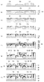
図1は、本発明の第1の実施の形態に係る半導体装置100の断面図である。以降の図において、同一の構成要素には同一の符号を付し、適宜説明を省略する。
半導体装置100は、基材20、半導体チップ10a、10b、チップ部品12a、12b、絶縁基材30、配線パターン34、ビアプラグ32、外部引出電極36、凹部40、樹脂50を含む。図1において、便宜上、基材20の設けられた面を下方向とし、凹部40が設けられた面を上方向とする。
この凹部40に実装された半導体チップ10bは、樹脂50による封止工程前であれば内部に形成される抵抗、コンデンサのトリミングを行うことができる。従って、半導体装置100の組み立て後においても、回路特性の調整を行うことができ、歩留まりの向上を図ることができる。
さらに、絶縁基材30内の配線導体層に形成された配線パターン34が凹部40から露出している場合には、この配線パターンをトリミングすることによっても回路定数を変更することができる。
その結果、半導体チップ10aおよびチップ部品12aは絶縁性樹脂膜122内に押しまれる。導電性膜120は、配線導体層となり、後の工程により配線パターンが形成される。
逆に、基材20を収縮させた状態で半導体チップ10aおよびチップ部品12aを絶縁性樹脂膜122内に押し込む場合には、素子間の間隔が狭くなるため、高密度な素子配置が可能となる。
以上の工程を経て、第1の実施の形態に係る半導体装置100を製造することができる。
第2の実施の形態に係る半導体装置200について、上述の半導体装置100との相違点を中心に説明する。図3は、第2の実施の形態に係る半導体装置200の断面図である。
半導体装置200は、基材20、半導体チップ10a、チップ部品12a、絶縁基材30、配線パターン34、ビアプラグ32、外部引出電極36を含む。図3においても、便宜上、基材20を下方向とし、外部引出電極36が設けられた面を上方向とする。
通常の半導体チップ10aの厚みは100〜300μmであり、抵抗やコンデンサ等のチップ部品12aの高さはいわゆる0603サイズで300μm、1005サイズで500μm程度である。本実施の形態では、半導体チップ10a等が実装されていない間隙部にも、配線導体層を形成して、より高密度な配線を行っている。
絶縁性樹脂膜122の開口部150は、配線パターン34cを形成する箇所に設けられる。
まず、図6(a)に示すように、基材20に半導体チップ10aおよびチップ部品12aをダイ、チップボンディングする。次いで、図6(b)に示すように、配線パターン34cを形成したい箇所に局所的に樹脂ポッティングを行い、絶縁体層130aを形成する。続いて図6(c)〜(e)に示すように配線パターン34c、絶縁体層130bの形成し、ビアプラグ32を形成する。
Claims (4)
- 高さの異なる複数の回路素子を固定した基材と、
前記基材上に、前記複数の回路素子が埋め込まれた第1の絶縁樹脂膜と、
前記基材からの厚みが均一になるように前記第1の絶縁樹脂膜上に配置された導電性膜からなり、前記複数の回路素子を互いに接続する第1の配線導体層と、
前記第1の絶縁樹脂膜及び前記第1の配線導体層上に、前記第1の絶縁樹脂膜よりも膜厚の薄い第2の絶縁樹脂膜及び第2の配線導体層からなる積層体を複数備えた多層構造体と、
前記第2の絶縁樹脂膜に備えられ、前記第1又は第2の配線導体層に到達した凹部と、
前記凹部に実装され前記第1又は第2の配線導体層と接続された回路素子と、を備えることを特徴とする回路装置。 - 高さの異なる複数の回路素子を固定した基材を準備する工程と、
第1の絶縁樹脂膜上に導電性膜を配置し、前記導電性膜に加圧して前記第1の絶縁樹脂膜側を前記基材に圧着することにより、前記複数の回路素子を前記第1の絶縁樹脂膜内に埋め込む工程と、
前記導電性膜をパターニングして第1の配線パターンを形成する工程と、
前記第1の絶縁樹脂膜に設けたビアプラグと、前記第1の配線パターンとにより前記複数の回路素子を互いに接続する工程と、
前記第1の絶縁樹脂膜及び前記第1の配線パターン上に、前記第1の絶縁樹脂膜よりも膜厚の薄い第2の絶縁樹脂膜及び第2の配線パターンを複数層備えた多層構造体を形成する工程と、
前記第2の絶縁樹脂膜に、前記第1又は第2の配線パターンが露出する凹部を形成する工程と、
を含むことを特徴とする回路装置の製造方法。 - さらに、前記凹部に回路素子を実装する工程を含むことを特徴とする請求項2に記載の回路装置の製造方法。
- さらに、前記凹部に樹脂を充填して前記回路素子を封止する工程を含むことを特徴とする請求項3に記載の回路装置の製造方法。
Priority Applications (3)
| Application Number | Priority Date | Filing Date | Title |
|---|---|---|---|
| JP2004253998A JP4252019B2 (ja) | 2004-09-01 | 2004-09-01 | 回路装置およびその製造方法 |
| US11/215,121 US7875980B2 (en) | 2004-09-01 | 2005-08-31 | Semiconductor device having laminated structure |
| CN2005100980208A CN1744314B (zh) | 2004-09-01 | 2005-09-01 | 具有层积结构的半导体装置及其制造方法 |
Applications Claiming Priority (1)
| Application Number | Priority Date | Filing Date | Title |
|---|---|---|---|
| JP2004253998A JP4252019B2 (ja) | 2004-09-01 | 2004-09-01 | 回路装置およびその製造方法 |
Related Child Applications (1)
| Application Number | Title | Priority Date | Filing Date |
|---|---|---|---|
| JP2008228563A Division JP2009033185A (ja) | 2008-09-05 | 2008-09-05 | 半導体装置およびその製造方法 |
Publications (2)
| Publication Number | Publication Date |
|---|---|
| JP2006073702A JP2006073702A (ja) | 2006-03-16 |
| JP4252019B2 true JP4252019B2 (ja) | 2009-04-08 |
Family
ID=35941943
Family Applications (1)
| Application Number | Title | Priority Date | Filing Date |
|---|---|---|---|
| JP2004253998A Expired - Fee Related JP4252019B2 (ja) | 2004-09-01 | 2004-09-01 | 回路装置およびその製造方法 |
Country Status (3)
| Country | Link |
|---|---|
| US (1) | US7875980B2 (ja) |
| JP (1) | JP4252019B2 (ja) |
| CN (1) | CN1744314B (ja) |
Families Citing this family (16)
| Publication number | Priority date | Publication date | Assignee | Title |
|---|---|---|---|---|
| US20090057903A1 (en) * | 2007-03-29 | 2009-03-05 | Yoshio Okayama | Semiconductor module, method for manufacturing semiconductor modules, semiconductor apparatus, method for manufacturing semiconductor apparatuses, and portable device |
| JP2008300560A (ja) * | 2007-05-30 | 2008-12-11 | Sony Corp | 半導体装置及びその製造方法 |
| KR100945285B1 (ko) * | 2007-09-18 | 2010-03-03 | 삼성전기주식회사 | 전자소자 내장 인쇄회로기판 및 그 제조 방법 |
| US8963341B2 (en) * | 2007-10-16 | 2015-02-24 | Edward Binkley | Process for placing, securing and interconnecting electronic components |
| US20110156261A1 (en) * | 2009-03-24 | 2011-06-30 | Christopher James Kapusta | Integrated circuit package and method of making same |
| US9299661B2 (en) * | 2009-03-24 | 2016-03-29 | General Electric Company | Integrated circuit package and method of making same |
| US20140000099A1 (en) * | 2012-06-29 | 2014-01-02 | Noah Austin Spivak | Methods for building resistive elements into printed circuit boards |
| JP2014116548A (ja) * | 2012-12-12 | 2014-06-26 | Ngk Spark Plug Co Ltd | 多層配線基板およびその製造方法 |
| US9185794B1 (en) * | 2013-07-31 | 2015-11-10 | Juniper Networks, Inc. | Apparatus and methods for placement of discrete components on internal printed circuit board layers |
| EP2881753B1 (en) | 2013-12-05 | 2019-03-06 | ams AG | Optical sensor arrangement and method of producing an optical sensor arrangement |
| EP2881983B1 (en) * | 2013-12-05 | 2019-09-18 | ams AG | Interposer-chip-arrangement for dense packaging of chips |
| CN105848416B (zh) * | 2016-03-31 | 2019-04-26 | 华为技术有限公司 | 一种基板及移动终端 |
| CN109892023B (zh) * | 2016-10-25 | 2022-03-22 | 株式会社村田制作所 | 电路模块 |
| US10541153B2 (en) * | 2017-08-03 | 2020-01-21 | General Electric Company | Electronics package with integrated interconnect structure and method of manufacturing thereof |
| CN114270714B (zh) * | 2019-08-28 | 2024-01-05 | 株式会社村田制作所 | 高频模块以及通信装置 |
| CN114361040B (zh) * | 2021-11-18 | 2023-03-24 | 珠海越亚半导体股份有限公司 | 一种双面互联嵌入式芯片封装结构及其制造方法 |
Family Cites Families (14)
| Publication number | Priority date | Publication date | Assignee | Title |
|---|---|---|---|---|
| JPS6375075A (ja) | 1986-09-18 | 1988-04-05 | Toyo Seikan Kaisha Ltd | 缶用水性塗料及び塗装缶体 |
| JPH065993A (ja) | 1992-06-17 | 1994-01-14 | Tanaka Kikinzoku Kogyo Kk | 内層回路露出型基板 |
| JPH08162486A (ja) | 1994-12-05 | 1996-06-21 | Shin Etsu Chem Co Ltd | 半導体素子の樹脂封止方法 |
| JP2701802B2 (ja) * | 1995-07-17 | 1998-01-21 | 日本電気株式会社 | ベアチップ実装用プリント基板 |
| JPH09162320A (ja) * | 1995-12-08 | 1997-06-20 | Shinko Electric Ind Co Ltd | 半導体パッケージおよび半導体装置 |
| US6038133A (en) * | 1997-11-25 | 2000-03-14 | Matsushita Electric Industrial Co., Ltd. | Circuit component built-in module and method for producing the same |
| DE10122705B4 (de) * | 2000-05-11 | 2012-07-26 | Mitutoyo Corp. | Einrichtung mit funktionalem Bauelement und Verfahren zu seiner Herstellung |
| JP4529262B2 (ja) | 2000-09-14 | 2010-08-25 | ソニー株式会社 | 高周波モジュール装置及びその製造方法 |
| JP2003142797A (ja) | 2001-11-02 | 2003-05-16 | Matsushita Electric Ind Co Ltd | 電子部品実装済完成品の製造方法及び電子部品実装済完成品 |
| TWI234253B (en) * | 2002-05-31 | 2005-06-11 | Fujitsu Ltd | Semiconductor device and manufacturing method thereof |
| JP3976089B2 (ja) * | 2002-08-09 | 2007-09-12 | 株式会社リコー | 半導体集積回路装置及びその製造方法 |
| JP4056854B2 (ja) * | 2002-11-05 | 2008-03-05 | 新光電気工業株式会社 | 半導体装置の製造方法 |
| JP4228677B2 (ja) * | 2002-12-06 | 2009-02-25 | パナソニック株式会社 | 回路基板 |
| JP2004273591A (ja) * | 2003-03-06 | 2004-09-30 | Seiko Epson Corp | 半導体装置及びその製造方法 |
-
2004
- 2004-09-01 JP JP2004253998A patent/JP4252019B2/ja not_active Expired - Fee Related
-
2005
- 2005-08-31 US US11/215,121 patent/US7875980B2/en not_active Expired - Fee Related
- 2005-09-01 CN CN2005100980208A patent/CN1744314B/zh not_active Expired - Fee Related
Also Published As
| Publication number | Publication date |
|---|---|
| US20060043606A1 (en) | 2006-03-02 |
| CN1744314A (zh) | 2006-03-08 |
| CN1744314B (zh) | 2011-05-04 |
| JP2006073702A (ja) | 2006-03-16 |
| US7875980B2 (en) | 2011-01-25 |
Similar Documents
| Publication | Publication Date | Title |
|---|---|---|
| JP4252019B2 (ja) | 回路装置およびその製造方法 | |
| US10141203B2 (en) | Electrical interconnect structure for an embedded electronics package | |
| US10098243B2 (en) | Printed wiring board and semiconductor package | |
| US7683268B2 (en) | Semiconductor module with high process accuracy, manufacturing method thereof, and semiconductor device therewith | |
| JP2010239150A (ja) | 半導体モジュールおよびその製造方法 | |
| CN1352804A (zh) | 高密度电子封装及其制造方法 | |
| US20250227849A1 (en) | Embedded component package structure and manufacturing method thereof | |
| KR101109356B1 (ko) | 임베디드 인쇄회로기판의 제조방법 | |
| CN101388383A (zh) | 半导体封装及其制造方法 | |
| US9299661B2 (en) | Integrated circuit package and method of making same | |
| CN101286463A (zh) | 半导体装置及其制造方法 | |
| US11445617B2 (en) | Package structure and manufacturing method thereof | |
| US10510638B2 (en) | Electronic component-embedded board | |
| JP4875925B2 (ja) | 多層配線板及びその製造方法 | |
| JP4880218B2 (ja) | 回路装置 | |
| JP2009033185A (ja) | 半導体装置およびその製造方法 | |
| JP2005129904A (ja) | 半導体装置およびその製造方法 | |
| KR20150043135A (ko) | 금속막을 포함한 인쇄회로기판 및 그것을 포함한 반도체 패키지 | |
| KR102787140B1 (ko) | 반도체 패키지 및 이의 제조방법 | |
| US20060193108A1 (en) | Circuit device and manufacturing method thereof | |
| CN100429767C (zh) | 元件搭载基板 | |
| JP2005109068A (ja) | 半導体装置およびその製造方法 | |
| US20240112978A1 (en) | Electronic package | |
| CN117998729A (zh) | 嵌埋器件封装基板及其制作方法 | |
| JP2005286146A (ja) | 半導体装置および半導体装置の製造方法 |
Legal Events
| Date | Code | Title | Description |
|---|---|---|---|
| A621 | Written request for application examination |
Free format text: JAPANESE INTERMEDIATE CODE: A621 Effective date: 20061012 |
|
| A977 | Report on retrieval |
Free format text: JAPANESE INTERMEDIATE CODE: A971007 Effective date: 20080704 |
|
| A131 | Notification of reasons for refusal |
Free format text: JAPANESE INTERMEDIATE CODE: A131 Effective date: 20080708 |
|
| A521 | Request for written amendment filed |
Free format text: JAPANESE INTERMEDIATE CODE: A523 Effective date: 20080908 |
|
| A131 | Notification of reasons for refusal |
Free format text: JAPANESE INTERMEDIATE CODE: A131 Effective date: 20080930 |
|
| A521 | Request for written amendment filed |
Free format text: JAPANESE INTERMEDIATE CODE: A523 Effective date: 20081201 |
|
| TRDD | Decision of grant or rejection written | ||
| A01 | Written decision to grant a patent or to grant a registration (utility model) |
Free format text: JAPANESE INTERMEDIATE CODE: A01 Effective date: 20081224 |
|
| A01 | Written decision to grant a patent or to grant a registration (utility model) |
Free format text: JAPANESE INTERMEDIATE CODE: A01 |
|
| A61 | First payment of annual fees (during grant procedure) |
Free format text: JAPANESE INTERMEDIATE CODE: A61 Effective date: 20090120 |
|
| FPAY | Renewal fee payment (event date is renewal date of database) |
Free format text: PAYMENT UNTIL: 20120130 Year of fee payment: 3 |
|
| FPAY | Renewal fee payment (event date is renewal date of database) |
Free format text: PAYMENT UNTIL: 20130130 Year of fee payment: 4 |
|
| FPAY | Renewal fee payment (event date is renewal date of database) |
Free format text: PAYMENT UNTIL: 20140130 Year of fee payment: 5 |
|
| LAPS | Cancellation because of no payment of annual fees |