JP4336593B2 - サーマルヘッド - Google Patents
サーマルヘッド Download PDFInfo
- Publication number
- JP4336593B2 JP4336593B2 JP2004032874A JP2004032874A JP4336593B2 JP 4336593 B2 JP4336593 B2 JP 4336593B2 JP 2004032874 A JP2004032874 A JP 2004032874A JP 2004032874 A JP2004032874 A JP 2004032874A JP 4336593 B2 JP4336593 B2 JP 4336593B2
- Authority
- JP
- Japan
- Prior art keywords
- substrate
- layer
- thermal head
- heat storage
- common electrode
- Prior art date
- Legal status (The legal status is an assumption and is not a legal conclusion. Google has not performed a legal analysis and makes no representation as to the accuracy of the status listed.)
- Expired - Fee Related
Links
- 239000000758 substrate Substances 0.000 claims description 90
- 238000005338 heat storage Methods 0.000 claims description 51
- 238000010438 heat treatment Methods 0.000 claims description 42
- 229910052721 tungsten Inorganic materials 0.000 claims description 14
- 229910052804 chromium Inorganic materials 0.000 claims description 11
- 229910052750 molybdenum Inorganic materials 0.000 claims description 11
- 229910052715 tantalum Inorganic materials 0.000 claims description 11
- 229910052719 titanium Inorganic materials 0.000 claims description 10
- 229910052758 niobium Inorganic materials 0.000 claims description 9
- 239000012535 impurity Substances 0.000 claims description 8
- 230000002093 peripheral effect Effects 0.000 claims description 7
- 239000000956 alloy Substances 0.000 claims description 6
- 238000007743 anodising Methods 0.000 claims 1
- 239000010410 layer Substances 0.000 description 166
- 230000004888 barrier function Effects 0.000 description 29
- 238000000034 method Methods 0.000 description 19
- 230000008569 process Effects 0.000 description 14
- 239000000463 material Substances 0.000 description 11
- 238000004519 manufacturing process Methods 0.000 description 10
- 229910004298 SiO 2 Inorganic materials 0.000 description 9
- 238000007639 printing Methods 0.000 description 9
- 238000004544 sputter deposition Methods 0.000 description 9
- 230000015572 biosynthetic process Effects 0.000 description 7
- 239000011810 insulating material Substances 0.000 description 7
- 239000011241 protective layer Substances 0.000 description 7
- 229910052723 transition metal Inorganic materials 0.000 description 7
- 150000003624 transition metals Chemical class 0.000 description 7
- 229910052782 aluminium Inorganic materials 0.000 description 6
- 238000000137 annealing Methods 0.000 description 6
- 229910052802 copper Inorganic materials 0.000 description 6
- 238000001020 plasma etching Methods 0.000 description 6
- ZOXJGFHDIHLPTG-UHFFFAOYSA-N Boron Chemical compound [B] ZOXJGFHDIHLPTG-UHFFFAOYSA-N 0.000 description 5
- 229910052796 boron Inorganic materials 0.000 description 5
- 238000005530 etching Methods 0.000 description 5
- 239000003870 refractory metal Substances 0.000 description 5
- 229910003564 SiAlON Inorganic materials 0.000 description 4
- 239000010407 anodic oxide Substances 0.000 description 4
- 238000001312 dry etching Methods 0.000 description 4
- 229910052814 silicon oxide Inorganic materials 0.000 description 4
- 230000001276 controlling effect Effects 0.000 description 3
- 238000009413 insulation Methods 0.000 description 3
- 230000003647 oxidation Effects 0.000 description 3
- 238000007254 oxidation reaction Methods 0.000 description 3
- -1 Ta 2 O 5 Inorganic materials 0.000 description 2
- 238000010292 electrical insulation Methods 0.000 description 2
- 230000017525 heat dissipation Effects 0.000 description 2
- 238000010884 ion-beam technique Methods 0.000 description 2
- 229910052742 iron Inorganic materials 0.000 description 2
- 229910052748 manganese Inorganic materials 0.000 description 2
- 239000000203 mixture Substances 0.000 description 2
- 229910052759 nickel Inorganic materials 0.000 description 2
- 238000000206 photolithography Methods 0.000 description 2
- 238000007740 vapor deposition Methods 0.000 description 2
- 229910052727 yttrium Inorganic materials 0.000 description 2
- 229910052726 zirconium Inorganic materials 0.000 description 2
- 229910017121 AlSiO Inorganic materials 0.000 description 1
- 229910001030 Iron–nickel alloy Inorganic materials 0.000 description 1
- 229910000676 Si alloy Inorganic materials 0.000 description 1
- 229910001362 Ta alloys Inorganic materials 0.000 description 1
- 238000005299 abrasion Methods 0.000 description 1
- 230000001133 acceleration Effects 0.000 description 1
- 229910045601 alloy Inorganic materials 0.000 description 1
- 229910010293 ceramic material Inorganic materials 0.000 description 1
- 239000011195 cermet Substances 0.000 description 1
- 230000008859 change Effects 0.000 description 1
- 150000001875 compounds Chemical class 0.000 description 1
- 238000000151 deposition Methods 0.000 description 1
- 230000008021 deposition Effects 0.000 description 1
- 238000005516 engineering process Methods 0.000 description 1
- 239000011521 glass Substances 0.000 description 1
- 230000020169 heat generation Effects 0.000 description 1
- 239000007769 metal material Substances 0.000 description 1
- 230000001105 regulatory effect Effects 0.000 description 1
- 238000007650 screen-printing Methods 0.000 description 1
- 239000004065 semiconductor Substances 0.000 description 1
- 238000009751 slip forming Methods 0.000 description 1
- 238000000992 sputter etching Methods 0.000 description 1
- 238000003860 storage Methods 0.000 description 1
- 239000000126 substance Substances 0.000 description 1
- 230000001629 suppression Effects 0.000 description 1
- 238000010301 surface-oxidation reaction Methods 0.000 description 1
Images


Classifications
-
- B—PERFORMING OPERATIONS; TRANSPORTING
- B41—PRINTING; LINING MACHINES; TYPEWRITERS; STAMPS
- B41J—TYPEWRITERS; SELECTIVE PRINTING MECHANISMS, i.e. MECHANISMS PRINTING OTHERWISE THAN FROM A FORME; CORRECTION OF TYPOGRAPHICAL ERRORS
- B41J2/00—Typewriters or selective printing mechanisms characterised by the printing or marking process for which they are designed
- B41J2/315—Typewriters or selective printing mechanisms characterised by the printing or marking process for which they are designed characterised by selective application of heat to a heat sensitive printing or impression-transfer material
- B41J2/32—Typewriters or selective printing mechanisms characterised by the printing or marking process for which they are designed characterised by selective application of heat to a heat sensitive printing or impression-transfer material using thermal heads
- B41J2/335—Structure of thermal heads
- B41J2/33505—Constructional details
- B41J2/3351—Electrode layers
-
- B—PERFORMING OPERATIONS; TRANSPORTING
- B41—PRINTING; LINING MACHINES; TYPEWRITERS; STAMPS
- B41J—TYPEWRITERS; SELECTIVE PRINTING MECHANISMS, i.e. MECHANISMS PRINTING OTHERWISE THAN FROM A FORME; CORRECTION OF TYPOGRAPHICAL ERRORS
- B41J2/00—Typewriters or selective printing mechanisms characterised by the printing or marking process for which they are designed
- B41J2/315—Typewriters or selective printing mechanisms characterised by the printing or marking process for which they are designed characterised by selective application of heat to a heat sensitive printing or impression-transfer material
- B41J2/32—Typewriters or selective printing mechanisms characterised by the printing or marking process for which they are designed characterised by selective application of heat to a heat sensitive printing or impression-transfer material using thermal heads
- B41J2/335—Structure of thermal heads
- B41J2/33505—Constructional details
- B41J2/33515—Heater layers
-
- B—PERFORMING OPERATIONS; TRANSPORTING
- B41—PRINTING; LINING MACHINES; TYPEWRITERS; STAMPS
- B41J—TYPEWRITERS; SELECTIVE PRINTING MECHANISMS, i.e. MECHANISMS PRINTING OTHERWISE THAN FROM A FORME; CORRECTION OF TYPOGRAPHICAL ERRORS
- B41J2/00—Typewriters or selective printing mechanisms characterised by the printing or marking process for which they are designed
- B41J2/315—Typewriters or selective printing mechanisms characterised by the printing or marking process for which they are designed characterised by selective application of heat to a heat sensitive printing or impression-transfer material
- B41J2/32—Typewriters or selective printing mechanisms characterised by the printing or marking process for which they are designed characterised by selective application of heat to a heat sensitive printing or impression-transfer material using thermal heads
- B41J2/335—Structure of thermal heads
- B41J2/33545—Structure of thermal heads characterised by dimensions
-
- B—PERFORMING OPERATIONS; TRANSPORTING
- B41—PRINTING; LINING MACHINES; TYPEWRITERS; STAMPS
- B41J—TYPEWRITERS; SELECTIVE PRINTING MECHANISMS, i.e. MECHANISMS PRINTING OTHERWISE THAN FROM A FORME; CORRECTION OF TYPOGRAPHICAL ERRORS
- B41J2/00—Typewriters or selective printing mechanisms characterised by the printing or marking process for which they are designed
- B41J2/315—Typewriters or selective printing mechanisms characterised by the printing or marking process for which they are designed characterised by selective application of heat to a heat sensitive printing or impression-transfer material
- B41J2/32—Typewriters or selective printing mechanisms characterised by the printing or marking process for which they are designed characterised by selective application of heat to a heat sensitive printing or impression-transfer material using thermal heads
- B41J2/335—Structure of thermal heads
- B41J2/3355—Structure of thermal heads characterised by materials
-
- B—PERFORMING OPERATIONS; TRANSPORTING
- B41—PRINTING; LINING MACHINES; TYPEWRITERS; STAMPS
- B41J—TYPEWRITERS; SELECTIVE PRINTING MECHANISMS, i.e. MECHANISMS PRINTING OTHERWISE THAN FROM A FORME; CORRECTION OF TYPOGRAPHICAL ERRORS
- B41J2/00—Typewriters or selective printing mechanisms characterised by the printing or marking process for which they are designed
- B41J2/315—Typewriters or selective printing mechanisms characterised by the printing or marking process for which they are designed characterised by selective application of heat to a heat sensitive printing or impression-transfer material
- B41J2/32—Typewriters or selective printing mechanisms characterised by the printing or marking process for which they are designed characterised by selective application of heat to a heat sensitive printing or impression-transfer material using thermal heads
- B41J2/335—Structure of thermal heads
- B41J2/3359—Manufacturing processes
Landscapes
- Engineering & Computer Science (AREA)
- Manufacturing & Machinery (AREA)
- Electronic Switches (AREA)
Description
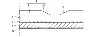
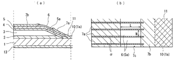
1a Si基板表面
1b 側端面(厚さ方向の周囲端面)
1c 背面
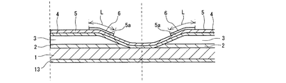
2 第1の絶縁層
3 蓄熱層
3a テーパーエッジ部
3b 均一膜厚部
4 第2の絶縁層
5 抵抗層
5a 発熱抵抗体
6 絶縁バリア層
7 電極層
7a コモン電極
7b 個別電極
7c 開放部
8 配線用Al電極
9 耐磨耗保護層
10 露出領域
11 コンタクト部
12 絶縁膜(Si陽極酸化膜)
13 絶縁膜
R レジスト層
α ギャップ領域
Claims (7)
- 基板表面上に積層形成された蓄熱層と、該蓄熱層上に形成された複数の発熱抵抗体と、各発熱抵抗体の抵抗長方向の一端部にそれぞれ導通接続する複数の個別電極と、全発熱抵抗体の抵抗長方向の他端部に導通接続するコモン電極とを有するサーマルヘッドにおいて、
前記基板は、比抵抗が20mΩ・cm以下のSi基板であること、
このSi基板上には前記蓄熱層の存在しない露出領域が備えられ、この露出領域上に、前記コモン電極と該Si基板表面とをオーミック接触させるコンタクト部を形成したこと、及び、
このコンタクト部は、Cr、Ta、Mo、W、Ti、Nbのいずれか、あるいは該Cr、Ta、Mo、W、Ti、Nbを主成分とする合金材料により形成されていること、
を特徴とするサーマルヘッド。 - 請求項1記載のサーマルヘッドにおいて、前記Si基板の比抵抗は1.0mΩ・cm以下であるサーマルヘッド。
- 請求項1又は2記載のサーマルヘッドにおいて、前記Si基板は不純物をドーピングしたp型Si基板であるサーマルヘッド。
- 請求項1ないし3のいずれか一項に記載のサーマルヘッドにおいて、前記Si基板背面及び前記Si基板の厚さ方向の周囲端面には、絶縁膜が形成されているサーマルヘッド。
- 請求項4記載のサーマルヘッドにおいて、前記Si基板の厚さ方向の周囲端面には、前記Si基板の陽極酸化による絶縁膜が形成されているサーマルヘッド。
- 請求項1ないし5のいずれか一項に記載のサーマルヘッドにおいて、前記蓄熱層の上下に絶縁層を備えたサーマルヘッド。
- 請求項1ないし6のいずれか一項に記載のサーマルヘッドにおいて、前記蓄熱層は、前記Si基板表面上に段差を与える均一膜厚部と、前記Si基板表面から該均一膜厚部に向けて徐々に膜厚が増大するテーパーエッジ部とを有しており、前記コモン電極は前記テーパーエッジ部の上方に位置しているサーマルヘッド。
Priority Applications (3)
| Application Number | Priority Date | Filing Date | Title |
|---|---|---|---|
| JP2004032874A JP4336593B2 (ja) | 2004-02-10 | 2004-02-10 | サーマルヘッド |
| US11/048,337 US7248275B2 (en) | 2004-02-10 | 2005-02-01 | Thermal head including Si substrate and method for manufacturing the same |
| CNB2005100090028A CN100352661C (zh) | 2004-02-10 | 2005-02-16 | 热敏头及其制造方法 |
Applications Claiming Priority (1)
| Application Number | Priority Date | Filing Date | Title |
|---|---|---|---|
| JP2004032874A JP4336593B2 (ja) | 2004-02-10 | 2004-02-10 | サーマルヘッド |
Publications (2)
| Publication Number | Publication Date |
|---|---|
| JP2005224950A JP2005224950A (ja) | 2005-08-25 |
| JP4336593B2 true JP4336593B2 (ja) | 2009-09-30 |
Family
ID=34824238
Family Applications (1)
| Application Number | Title | Priority Date | Filing Date |
|---|---|---|---|
| JP2004032874A Expired - Fee Related JP4336593B2 (ja) | 2004-02-10 | 2004-02-10 | サーマルヘッド |
Country Status (3)
| Country | Link |
|---|---|
| US (1) | US7248275B2 (ja) |
| JP (1) | JP4336593B2 (ja) |
| CN (1) | CN100352661C (ja) |
Families Citing this family (12)
| Publication number | Priority date | Publication date | Assignee | Title |
|---|---|---|---|---|
| JP2012096459A (ja) * | 2010-11-02 | 2012-05-24 | Tdk Corp | サーマルヘッド及びこれを用いたサーマルプリンタ |
| US9061520B2 (en) * | 2011-01-25 | 2015-06-23 | Kyocera Corporation | Thermal head and thermal printer including the same |
| JP2013082092A (ja) * | 2011-10-06 | 2013-05-09 | Seiko Instruments Inc | サーマルヘッドおよびその製造方法、並びにサーマルプリンタ |
| JP6021142B2 (ja) * | 2012-06-19 | 2016-11-09 | セイコーインスツル株式会社 | サーマルヘッド、プリンタおよびサーマルヘッドの製造方法 |
| JP2017114057A (ja) * | 2015-12-25 | 2017-06-29 | ローム株式会社 | サーマルプリントヘッド |
| JP2017114051A (ja) * | 2015-12-25 | 2017-06-29 | ローム株式会社 | サーマルプリントヘッド |
| JP6650264B2 (ja) * | 2015-12-25 | 2020-02-19 | ローム株式会社 | サーマルプリントヘッド |
| JP6867768B2 (ja) * | 2016-09-15 | 2021-05-12 | ローム株式会社 | サーマルプリントヘッド |
| EP3529083B1 (en) * | 2017-03-15 | 2022-01-12 | Hewlett-Packard Development Company, L.P. | Thermal contact dies |
| JP2020073343A (ja) * | 2020-02-04 | 2020-05-14 | ローム株式会社 | サーマルプリントヘッド |
| JP6842576B2 (ja) * | 2020-02-04 | 2021-03-17 | ローム株式会社 | サーマルプリントヘッド |
| JP7545828B2 (ja) * | 2020-08-04 | 2024-09-05 | ローム株式会社 | サーマルプリントヘッド |
Family Cites Families (11)
| Publication number | Priority date | Publication date | Assignee | Title |
|---|---|---|---|---|
| DE3685983T2 (de) * | 1985-04-13 | 1993-02-25 | Konishiroku Photo Ind | Integrierte halbleiteranordnung. |
| US4635075A (en) * | 1985-12-04 | 1987-01-06 | Datametrics Corporation | Thermal print head and process for producing |
| JP2825870B2 (ja) * | 1989-08-31 | 1998-11-18 | 京セラ株式会社 | サーマルヘッド |
| JPH0584949A (ja) * | 1991-09-30 | 1993-04-06 | Kyocera Corp | サーマルヘツドの製造方法 |
| JPH05270036A (ja) * | 1992-03-27 | 1993-10-19 | Rohm Co Ltd | サーマルプリントヘッド |
| JPH0661947A (ja) | 1992-08-05 | 1994-03-04 | Fujitsu Ltd | 光空間伝送方式 |
| EP0711669B1 (en) * | 1994-05-31 | 1998-08-12 | Rohm Co., Ltd. | Thermal printhead |
| JP3298794B2 (ja) | 1996-07-24 | 2002-07-08 | アルプス電気株式会社 | サーマルヘッドおよびその製造方法 |
| US6201558B1 (en) * | 1998-05-08 | 2001-03-13 | Alps Electric Co., Ltd. | Thermal head |
| DE60034186T2 (de) * | 1999-02-18 | 2007-12-20 | Rohm Co. Ltd., Kyoto | Thermokopf und herstellungsverfahren |
| JP2003266754A (ja) * | 2002-03-19 | 2003-09-24 | Sii P & S Inc | サーマルヘッド |
-
2004
- 2004-02-10 JP JP2004032874A patent/JP4336593B2/ja not_active Expired - Fee Related
-
2005
- 2005-02-01 US US11/048,337 patent/US7248275B2/en not_active Expired - Lifetime
- 2005-02-16 CN CNB2005100090028A patent/CN100352661C/zh not_active Expired - Fee Related
Also Published As
| Publication number | Publication date |
|---|---|
| CN100352661C (zh) | 2007-12-05 |
| CN1654221A (zh) | 2005-08-17 |
| US20050174502A1 (en) | 2005-08-11 |
| US7248275B2 (en) | 2007-07-24 |
| JP2005224950A (ja) | 2005-08-25 |
Similar Documents
| Publication | Publication Date | Title |
|---|---|---|
| US7170539B2 (en) | Thermal head, method for manufacturing the same, and method for adjusting dot aspect ratio of thermal head | |
| JP4336593B2 (ja) | サーマルヘッド | |
| JP3069247B2 (ja) | サーマルヘッド | |
| US6767081B2 (en) | Thermal head | |
| JP3124873B2 (ja) | サーマルヘッドおよびその製造方法 | |
| JP4633442B2 (ja) | サーマルヘッド | |
| CN114905862B (zh) | 薄膜热敏打印头用发热基板及其制作方法 | |
| US6501497B2 (en) | Thermal head with small size of steps of protective layer formed on heating portion and manufacturing method thereof | |
| JP5199808B2 (ja) | サーマルヘッドの製造方法 | |
| JP3298780B2 (ja) | サーマルヘッドおよびサーマルヘッドの製造方法 | |
| JP4541229B2 (ja) | サーマルヘッド及びその製造方法 | |
| US6201558B1 (en) | Thermal head | |
| JP2004155160A (ja) | サーマルヘッド及びその製造方法 | |
| JPH07214808A (ja) | 薄膜型サーマルプリントヘッドおよびその製造方法 | |
| JP3231951B2 (ja) | サーマルヘッドおよびその製造方法 | |
| JPH10100460A (ja) | サーマルヘッドおよびその製造方法 | |
| JP3298794B2 (ja) | サーマルヘッドおよびその製造方法 | |
| US6330014B1 (en) | Thermal head manufactured by sequentially laminating conductive layer, layer insulating layer and heater element on heat insulating layer | |
| JP4307981B2 (ja) | サーマルヘッドの製造方法 | |
| JPH03239562A (ja) | サーマルヘッド | |
| JPH03234672A (ja) | サーマルヘッド | |
| JP3683745B2 (ja) | サーマルヘッド | |
| JP2000289240A (ja) | サーマルヘッド | |
| JP2005254461A (ja) | サーマルヘッド | |
| JP2003182127A (ja) | サーマルヘッド |
Legal Events
| Date | Code | Title | Description |
|---|---|---|---|
| A621 | Written request for application examination |
Free format text: JAPANESE INTERMEDIATE CODE: A621 Effective date: 20060906 |
|
| A977 | Report on retrieval |
Free format text: JAPANESE INTERMEDIATE CODE: A971007 Effective date: 20090312 |
|
| A131 | Notification of reasons for refusal |
Free format text: JAPANESE INTERMEDIATE CODE: A131 Effective date: 20090317 |
|
| A521 | Request for written amendment filed |
Free format text: JAPANESE INTERMEDIATE CODE: A523 Effective date: 20090427 |
|
| TRDD | Decision of grant or rejection written | ||
| A01 | Written decision to grant a patent or to grant a registration (utility model) |
Free format text: JAPANESE INTERMEDIATE CODE: A01 Effective date: 20090616 |
|
| A01 | Written decision to grant a patent or to grant a registration (utility model) |
Free format text: JAPANESE INTERMEDIATE CODE: A01 |
|
| A61 | First payment of annual fees (during grant procedure) |
Free format text: JAPANESE INTERMEDIATE CODE: A61 Effective date: 20090629 |
|
| FPAY | Renewal fee payment (event date is renewal date of database) |
Free format text: PAYMENT UNTIL: 20120703 Year of fee payment: 3 |
|
| R150 | Certificate of patent or registration of utility model |
Ref document number: 4336593 Country of ref document: JP Free format text: JAPANESE INTERMEDIATE CODE: R150 Free format text: JAPANESE INTERMEDIATE CODE: R150 |
|
| FPAY | Renewal fee payment (event date is renewal date of database) |
Free format text: PAYMENT UNTIL: 20130703 Year of fee payment: 4 |
|
| S533 | Written request for registration of change of name |
Free format text: JAPANESE INTERMEDIATE CODE: R313533 |
|
| R350 | Written notification of registration of transfer |
Free format text: JAPANESE INTERMEDIATE CODE: R350 |
|
| LAPS | Cancellation because of no payment of annual fees |