JP4336790B2 - Clock switching method and clock switching device - Google Patents
Clock switching method and clock switching device Download PDFInfo
- Publication number
- JP4336790B2 JP4336790B2 JP2002342362A JP2002342362A JP4336790B2 JP 4336790 B2 JP4336790 B2 JP 4336790B2 JP 2002342362 A JP2002342362 A JP 2002342362A JP 2002342362 A JP2002342362 A JP 2002342362A JP 4336790 B2 JP4336790 B2 JP 4336790B2
- Authority
- JP
- Japan
- Prior art keywords
- circuit
- clock
- selection
- interface unit
- output
- Prior art date
- Legal status (The legal status is an assumption and is not a legal conclusion. Google has not performed a legal analysis and makes no representation as to the accuracy of the status listed.)
- Expired - Fee Related
Links
- 238000000034 method Methods 0.000 title claims description 12
- 230000001360 synchronised effect Effects 0.000 claims description 88
- 238000000605 extraction Methods 0.000 claims description 55
- 238000006243 chemical reaction Methods 0.000 claims description 36
- 230000005540 biological transmission Effects 0.000 claims description 19
- 230000001419 dependent effect Effects 0.000 claims 1
- 238000010521 absorption reaction Methods 0.000 description 16
- 238000005070 sampling Methods 0.000 description 8
- 230000000694 effects Effects 0.000 description 3
- 230000006870 function Effects 0.000 description 2
- 238000013139 quantization Methods 0.000 description 2
- 230000000630 rising effect Effects 0.000 description 2
- 230000002159 abnormal effect Effects 0.000 description 1
- 238000007796 conventional method Methods 0.000 description 1
- 238000010586 diagram Methods 0.000 description 1
- 238000012423 maintenance Methods 0.000 description 1
- 230000002093 peripheral effect Effects 0.000 description 1
- 230000004044 response Effects 0.000 description 1
Images





Landscapes
- Synchronisation In Digital Transmission Systems (AREA)
- Stabilization Of Oscillater, Synchronisation, Frequency Synthesizers (AREA)
Description
【0001】
【発明の属する技術分野】
本発明はクロック切替方法及びクロック切替装置に関し、特にクロック切替によって伝送信号エラーが発生することなく切替を行うクロック切替方法及びクロック切替装置に関する。
【0002】
【従来の技術】
無線伝送装置においては、装置での信号処理を簡易化する為に入力信号からクロック抽出を行い、装置内クロックとして用いる。装置内のクロックはPLL回路を用いて入力信号に同期したクロックを生成するが、複数の入力信号がある場合には、任意の入力信号を同期源として装置内クロックを生成し、この装置内クロックで他の入力信号を同期化して伝送する。一方、複数の入力信号を装置内クロックで同期化する為の入力インタフェース部が必要となる。しかし、装置へ実装出来るサイズ等で入力インタフェース部の大きさには限界があり、全ての入力信号を1枚の入力インタフェース部にて同期化する事は出来ず、複数枚の入力インタフェース部を用いて同期化を行う。
【0003】
この為に、装置内クロック生成用同期源とする入力信号が障害により劣化した場合や、入力インタフェース部を保守の為に装置から取り外す際には、取り外さない入力インタフェース部に装置内クロック同期源を切替える必要がある。この装置内クロック同期源の切替を無瞬断で行う為にディジタルサンプリングPLL回路を用いる。このディジタルサンプリングPLL回路を用いることで、ライン抽出として利用する入力信号切替時にも装置内クロックの周波数変動を抑圧することができ、他の伝送信号では不要なデータ誤りが発生しない。しかし、ディジタルサンプリングPLL回路は、位相差をディジタル化する際の量子化誤差や回路構成上の実現性からサンプリングデータの下位X(X≧1)ビットを除いた値を用いて位相制御を行うため、装置内クロック同期源を切替えると以下の問題が発生する。
【0004】
ここで、従来例として入力インタフェース部211、212が図9となるもので構成された装置の現用第1無線回線を含む現用第1回線(図1)を用いて図10〜12を参照して説明する。装置内クロック同期源が入力信号11 201の場合には、入力インタフェース部211では、変換回路101にて入力信号11201から抽出したクロックが抽出選択回路104に送出され、抽出選択回路104では位相制御部41からの制御信号221を用いて選択され、選択回路105に送出される。選択回路105では、制御信号221を用いて入力インタフェース部211内の抽出選択回路104からの抽出選択クロック220を選択し、ディジタルPLL回路106に送出する。ディジタルPLL回路106では、選択回路105の選択出力222に同期したクロック、フレームパルス(以下、FP)を生成し、入力インタフェース部211内の多重化回路103に送出する。
【0005】
一方、入力インタフェース部212でも同様に制御信号221から選択回路105にて、入力インタフェース部211からの抽出選択クロック220を選択し、ディジタルPLL回路106に送出する。ディジタルPLL回路106では、選択回路105の選択出力222に同期したクロック、FPを生成し、入力インタフェース部212内の多重化回路103に送出する。この時のディジタルPLL回路106を図10で示し、回路動作を図11を用いて説明する。分周器N301では、選択出力222をN(N≧2)分周し、N分周出力401として位相比較回路303に送出する。分周器M302では、電圧制御発信器311の出力クロック406をM(M≧2)分周したM分周出力402を位相比較回路303に送出する。位相比較回路303ではN分周出力401とM分周出力402の位相差を比較し位相比較結果403をA/D変換回路306にて変換してカウント値404”a”(下位X(X≧2)ビットを除いた値は”A”)となる。タイミング生成回路305のタイミング信号(タイミングクロック)を用いて位相記憶回路307では、カウント値404”a”を記憶値405”a”として記憶する。この動作が入力インタフェース部211と入力インタフェース部212それぞれで行われ、入力インタフェース部211と入力インタフェース部212それぞれの分周器P315の出力FP407の位相差が”0”となる。
【0006】
図12の時刻t1’’時に装置内クロック同期源の切替が発生すると、入力インタフェース部211のディジタルPLL回路106では、制御回路313は、制御信号408を”H”として位相保持状態とし、選択回路T308の出力をA/D変換回路306のカウント値404”a”から位相記憶回路307の記憶値405”a”の切替を行いD/A変換回路309に送出し、位相記憶回路307の記憶値405”a”をサンプリングクロックで更新しないように保持するモードとなる。
【0007】
次に、分周器N301のN分周出力401の位置が従来t2’’の位置だったものが装置内クロック同期源の切替により、t3’’の位置に変動する。A/D変換回路306の時刻t3’’からt4’’までのカウント値404は、時刻t5’’で”a”から”b”(下位Xビットを除いた値は”B”)となり、比較回路314では、カウント値404”b”の下位Xビットを除いた値”B”と記憶値405”a”の下位Xビットを除いた値”A”を比較し、比較結果409を”LT”として送出する。これにより、制御回路313が分周器M302を制御しM分周出力402の位相を時刻t7’’からt8’’に変更する。時刻t5’’からt9’’までのA/D変換回路306のカウント値404は”e”(下位Xビットを除いた値は”A”)となる。時刻t9’’の時は、比較回路314では、カウント値404”e”の下位Xビットを除いた値”A”と記憶値405”a”の下位Xビットを除いた値”A”を比較し、カウント値404と記憶値405が一致するので比較結果409を”EQ”として制御回路313に送出する。制御回路313では、比較結果409”EQ”となると制御信号408を”L”として選択回路T308の出力を記憶値405”a”からカウント値404”e”に切替え、位相記憶回路307の記憶値405の保持状態を解除し位相保持動作を終了する。
【0008】
その後、ディジタルPLL回路106は通常動作となり、一定の時間経過後の時刻t10’’には、カウント値404”a”となるのでθ3’’=θ1’’となる(図11、図12)。同様に入力インタフェース部212でも装置内クロック同期源の切替が発生し、位相保持動作後に制御が行われる。ただし、時刻t5’’からt9’’までのA/D変換回路306のカウント値404は”f”(下位Xビットを除いた値は”A”)となり、その後制御を解除して時刻t10’’時にはθ3’’=θ1’’となる。
【0009】
【特許文献1】
特開平11−27247号公報(請求項1、図1)
【0010】
【発明が解決しようとする課題】
しかし、この従来技術には、次のような問題点があった。
【0011】
第1の問題点は、2つの入力インタフェース部211、212内の分周器P315の出力FP407の位相が変動することである。その理由は、装置内クロック同期源の切替が発生し、定常状態となると、ディジタルPLL回路106の動作によってθ3’’=θ1’’となるが、入力インタフェース部211のディジタルPLL回路106の出力FP407と入力インタフェース部212のディジタルPLL回路106の出力FP407に位相差θ4’’(図12)が発生し、位相差が一定とならない。これは、2枚の入力インタフェース部211、212のディジタルPLL回路106が独立で動作しているためであり、それぞれのディジタルPLL回路106の制御動作やサンプリングクロックが非同期であること、またサンプリングクロックの量子化誤差や回路構成上の実現性からカウント値404と記憶値405の下位Xビットを除いた値で比較を行うために図12のように時刻t5’’からt9’’までのA/D変換回路306のカウント値404は”e”と”f”であるが、下位Xビットを除いた値は同じ”a”となり一致とみなし制御が終わる。その後、時刻t10’’では、”e”と”f”の値分の位相差が発生する。この位相差は切替が発生する度に発生し累積する。このFPは多重化回路103から位相制御部41に出力され、位相制御部41(図4)内の位相吸収回路108のPLL回路110の同期源として用いられ位相吸収回路108で2枚の入力インタフェース部211、212の位相差を吸収後に変調部51に送出される。位相吸収回路108はある範囲の位相差までは位相吸収可能であり装置内同期クロック源の切替が発生しても伝送信号を誤り無く伝えることが可能であるが、位相差が位相吸収回路108の位相吸収範囲を超えると装置内クロック同期源の切替時に伝送信号に誤りを生じる。
【0012】
第2の問題点は、伝送時の遅延が増加することである。その理由は、第1の問題点を解決するために位相制御部41内の位相吸収回路108で位相吸収範囲を大きくするためにメモリを増やす方法が考えられる。しかし位相吸収範囲を大きくすると大量にメモリに書き込み、読み出す事となるので、多重化時に信号の遅延が増加することになる。また、メモリを増やしても有限であり、その位相吸収範囲を超えてしまうと伝送信号に誤りを生じる。
【0013】
本発明は、以上の問題点を解決する装置内クロック切替方法及び装置を提供する。
【0014】
【課題を解決するための手段】
本発明のクロック切替方法は、伝送装置における第1の入力インタフェース部から第2の入力インタフェース部へクロックを切替えるクロック切替方法であって、第1の入力インタフェース部への複数の入力信号からの一つを第1の同期クロック源として選択し、第1の抽出選択クロックとして送出する工程と、第2の入力インタフェース部への複数の入力信号からの一つを第2の同期クロック源として選択し、第2の抽出選択クロックとして送出する工程と、第1の選択回路において第1の抽出選択クロックおよび第2の抽出選択クロックのいずれかを選択して第1の選択出力として送出する工程と、第2の選択回路において第1の抽出選択クロックおよび第2の抽出選択クロックのいずれかを選択して第2の選択出力として送出する工程と、第1のディジタルPLL回路において、第1の選択出力に同期した、第1の同期クロックと第1の同期FPの生成を行い、第1の入力インタフェース部及び第2の入力インタフェース部に送出する工程と、第2のディジタルPLL回路において、第2の選択出力に同期した、第2の同期クロックと第2の同期FPの生成を行い、第1の入力インタフェース部及び第2の入力インタフェース部に送出する工程と、第1の入力インタフェース部において、第1の同期クロックおよび第1の同期FP、又は第2の同期クロックおよび第2の同期FP、のいずれかを選択して送出する工程と、第2の入力インタフェース部において、第1の同期クロックおよび第1の同期FP、又は第2の同期クロックおよび第2の同期FP、のいずれかを選択して送出する工程と、第1の同期FPの位相と第2の同期FPの位相が同じになるように制御する第1の制御出力を生成して、第1のディジタルPLL回路に送出する工程と、第1の同期FPの位相と第2の同期FPの位相が同じになるように制御する第2の制御出力を生成して、第2のディジタルPLL回路に送出する工程と、を備えることを特徴とする。
【0020】
本発明のクロック切替装置は、伝送装置における第1の入力インタフェース部から第2の入力インタフェース部へクロックを切替えるクロック切替装置であって、第1のインタフェース部は、第1の抽出選択回路と、第1の選択回路と、第1のディジタルPLL回路と、第1のクロック切替回路と、第1の従属制御回路とを備え、第2のインタフェース部は、第2の抽出選択回路と、第2の選択回路と、第2のディジタルPLL回路と、第2のクロック切替回路と、第2の従属制御回路とを備え、第1の抽出選択回路は、第1の入力インタフェース部への複数の入力信号からの一つを第1の同期クロック源として選択し、第1の抽出選択クロックとして第1の選択回路および第2の選択回路へ送出し、第2の抽出選択回路は、第2の入力インタフェース部への複数の入力信号からの一つを第2の同期クロック源として選択し、第2の抽出選択クロックとして第1の選択回路および第2の選択回路へ送出し、第1の選択回路は、第1の抽出選択クロックおよび第2の抽出選択クロックのいずれかを選択して第1の選択出力として第1のディジタルPLL回路へ送出し、第2の選択回路は、第1の抽出選択クロックおよび第2の抽出選択クロックのいずれかを選択して第2の選択出力として第2のディジタルPLL回路へ送出し、第1のディジタルPLL回路は、第1の選択出力に同期した、第1の同期クロックと第1の同期FPの生成を行い、第1の入力インタフェース部及び第2の入力インタフェース部に送出し、第2のディジタルPLL回路は、第2の選択出力に同期した、第2の同期クロックと第2の同期FPの生成を行い、第1のクロック切替回路および第2のクロック切替回路へ送出し、第1のクロック切替回路は、第1の同期クロックおよび第1の同期FP、又は第2の同期クロックおよび第2の同期FP、のいずれかを選択して送出し、第2のクロック切替回路は、第1の同期クロックおよび第1の同期FP、又は第2の同期クロックおよび第2の同期FP、のいずれかを選択して送出し、
第1の従属制御回路は、第1の同期FPの位相と第2の同期FPの位相が同じになるように制御する第1の制御出力を生成して、第1のディジタルPLL回路に送出し、
第2の従属制御回路は、第1の同期FPの位相と第2の同期FPの位相が同じになるように制御する第2の制御出力を生成して、第2のディジタルPLL回路に送出する、ことを特徴とする。
【0021】
本発明のクロック切替装置においては、ディジタルPLL回路が、選択回路の選択出力をN(N≧2)分周したN分周出力を送出する分周器Nと、クロックをM(M≧2)分周したM分周出力を送出する分周器Mと、N分周出力及びM分周出力の位相比較を行い、位相比較結果を送出する位相比較回路と、位相比較結果をカウントし、カウント値を送出するA/D変換回路と、カウント値を記憶し記憶値として送出する位相記憶回路と、カウント値及び記憶値の選択出力を選択値として送出する選択回路Tと、選択値をD/A変換してアナログ電圧を生成して送出するD/A変換回路と、アナログ電圧に含まれる不要な周波数成分を抑圧して送出するループフィルタと、ループフィルタから送出された電圧に従って周波数を制御した前記クロックを送出する電圧制御発信器と、クロックをP(P≧2)分周して生成したFPを送出する分周器Pと、カウント値と記憶値の比較を行い比較結果を送出する比較回路と、選択回路T、位相記憶回路、分周器Mを制御する制御回路と、を備えることを特徴とする。
【0022】
【発明の実施の形態】
次に、本発明の実施の形態について図面を参照して詳細に説明する。本発明によるクロック切替は、装置内同期クロック源として選択した一方の入力インタフェース部のディジタルPLL回路にて生成したクロックとフレームパルス(以下、FP)を他方の入力インタフェース部に供給することで装置内のクロックを1つのディジタルPLLで生成し、他方の入力インタフェース部ではクロック切替回路(図2の112)にて供給されたクロックとFPを選択して入力信号の多重化を行い、従属制御回路(図2の113)にてディジタルPLL回路(図2の106)で生成するFPの位相が供給FPと一意の位相関係となる制御信号の生成を行い、この制御信号をディジタルPLL回路(図2の106)に用いることで、装置内クロック同期源の切替となりクロックとFPを供給する入力インタフェース部の切替が発生しても、FPが一意の位相関係にある為、伝送信号にエラーが発生しないクロック切替を実現する。
【0023】
図1〜4において入力信号を多重化して伝送する現用N(N≧2)回線を有する無線伝送装置において、入力信号11 201を装置内クロック同期源として選択するので入力インタフェース部211がマスター動作となり、入力インタフェース部212がスレーブ動作になるものとする。定常状態では、装置内クロック同期源となる入力信号11 201を処理する入力インタフェース部211においてはマスター動作となるので、入力信号11 201は変換回路101で変換され、位相制御部41からの制御信号221を用いて抽出選択回路104、選択回路105で装置内クロック同期源として選択され、ディジタルPLL回路106に送出される。ディジタルPLL回路106では、ディジタルPLLを用いて入力信号11 201に同期したクロックとFPを生成し、クロック切替回路112と他方の入力インタフェース部212内のクロック切替回路112に送出する。この時ディジタルPLL回路106では、同期源となる選択出力222を分周器N301で分周したN分周出力401と電圧制御発信器311の出力クロック406を分周器M302で分周したM分周出力402から位相比較回路303、A/D変換回路306を用いて位相差を測定し、位相記憶回路307にて記憶を行う。クロック切替回路112は、マスター動作から従属制御回路113からの制御出力224を用いて入力インタフェース部211にて生成したクロックとFPを選択し多重化回路103に送出する。また、従属制御回路113の制御信号227は、マスター動作から入力インタフェース部211内のディジタルPLL回路106内の分周器P312の制御を行わない。
一方、入力インタフェース部212においてはスレーブ動作となるので、位相制御部41からの制御信号221を用いて入力インタフェース部211の抽出選択クロック220を選択しディジタルPLL回路106に送出する。ディジタルPLL回路106は、選択出力222に同期したクロックとFPを生成し、クロック切替回路112と入力インタフェース部211内のクロック切替回路112に送出する。この時のディジタルPLL回路106では入力インタフェース部211同様に位相差を位相記憶回路307にて記憶を行う。クロック切替回路112は、従属制御回路113からの制御出力224を用いて入力インタフェース部211にて生成したクロックとFPを選択し多重化回路103に送出する。また、スレーブ動作から従属制御回路113の制御出力227がディジタルPLL回路106内の分周器P312の制御を行って入力インタフェース部211のFPと一意の位相となるようにFPの位相制御を行う。
【0024】
装置内クロック同期源が入力信号11から入力信号15に切替が発生すると、入力インタフェース部211、212では、ディジタルPLL回路106内においては、制御回路313は定常状態時に位相記憶回路307で記憶した値を用いて装置内クロック同期源切替が発生する前の状態を保持し、位相制御部41からの制御信号221から選択回路105においてディジタルPLL出力の切替えを行い、位相比較回路303、A/D変換回路306を用いて、同期クロック源切替後の分周器N301のN分周出力401と分周器M302のM分周出力402の位相差を測定し、分周器M302を制御することで分周器M302のM分周出力402の位相を変化させ定常状態時に記憶した値と一致する制御を行う。一致後一定時間経過すると、入力インタフェース部211内の従属制御回路113ではマスター動作からスレーブ動作への切替が発生し、クロック切替回路112では多重化回路103への出力を入力インタフェース部211のディジタルPLL出力223から入力インタフェース部212のディジタルPLL出力229への切替信号を送出する。また、ディジタルPLL回路106に送出した制御出力227は入力インタフェース部211のFPと一意の位相となる様な位相制御を開始する。
【0025】
一方、入力インタフェース部212の従属制御回路113ではスレーブ動作からマスター動作となり、クロック切替回路112では、多重化回路103への出力を入力インタフェース部211のディジタルPLL出力223から入力インタフェース部212のディジタルPLL出力229への切替信号を送出する。また、ディジタルPLL回路106に送出した制御信号227で行ったFP位相制御を停止する。
【0026】
これにより、入力インタフェース部211、212間の装置内同期クロック源の切替えが発生しても、入力インタフェース部211、212の多重化回路103の出力位相を一意の位相関係に保つことで位相制御部41の位相吸収回路108にて装置内同期クロック源切替が発生してもFPの位相が位相吸収回路108の位相吸収範囲以内に保たれる為、FPの位相変動による伝送信号エラーを発生することなく装置内クロック切替が可能となる。
【0027】
本発明による装置内同期クロック切替方法及び装置は、装置内クロック同期源として選択した一方の入力インタフェース部のディジタルPLL回路で生成したクロックとFPを他方の入力インタフェース部へ供給することで装置内クロックを同一化し、他方のディジタルPLL回路で生成するFPを一意の位相関係に制御することにより、複数の入力インタフェース部から位相制御部41への出力位相を一定に保つことができる。これにより、クロック切替が発生しても入力インタフェース部のFPは、位相制御部41内の位相吸収回路108の位相吸収範囲内に納めることが出来るのでクロック切替によってエラーが発生することなく切替を行うことができるものである。
【0028】
上記した本発明の実施の形態を更に詳細に説明すべく、本発明の実施例を以下に図面を参照して説明する。
【0029】
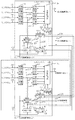
第1の実施形態:図1は、本発明実施例の無線伝送装置の装置構成ブロック図を示す。図2は装置内の入力インタフェース部211、212、図3は入力インタフェース部211、212内のディジタルPLL回路106であり、図4は、位相制御部41である。
【0030】
図1の現用第1無線回線を含む現用第1回線は、入力信号111〜114、入力信号115〜118、入力インタフェース部211、212、位相制御部41、変調部51、送信部61、受信部71、復調部81、分配部91、出力インタフェース部1011、1012、出力信号1111〜1114、出力信号1115〜1118を含んで構成される。現用第2、3、N無線回線を含む現用第2、3、N回線も同様の構成である。
【0031】
本発明は、図1の現用第1無線回線を含む現用第1回線の入力インタフェース部211、212、位相制御部41、変調部51を取り上げて説明するが、現用第2無線回線、現用第3無線回線、現用第N無線回線の入力インタフェース部221、222、231、232、2N1、2N2なども同様の構成、機能である。
【0032】
入力インタフェース部211、212においては、変換回路101では、入力信号11〜14、入力信号15〜18を伝送路バイポーラ信号を装置にて処理しやすいユニポーラ信号に変換してからフレーム同期を確立し、ユニポーラ信号に変換したデータ・フレームパルス(以下、FP)・クロックを記憶回路102に送出し、クロックを抽出選択回路104に送出する。
【0033】
記憶回路102では、変換回路101から送出されたデータをメモリーに書き込み、後述する多重化回路103からのクロックによってデータの読み出しを行う。
【0034】
多重化回路103では、後述するクロック切替回路112から送出されたクロックとFPを用いて記憶回路102のデータを読み出して多重化を行い位相制御部41に送出する。
【0035】
抽出選択回路104では、位相制御部41からの制御信号(HW(ハイウェイ)選択信号)221を用いて複数の入力信号11〜14(入力信号15〜18)から1つを同期クロック源として選択し、抽出選択クロック220(抽出選択クロック219)として選択回路105と他方入力インタフェース部212の選択回路105に送出し、入力信号11〜14が選択可能かを表す抽出クロック情報210を位相制御部41に送出する。
【0036】
選択回路105は、制御信号221を用いて自パネル抽出選択回路104の抽出選択クロック220または、他方入力インタフェース部212の抽出選択回路104の抽出選択クロック219のいずれかを選択して選択出力222としてディジタルPLL回路106に送出する。
【0037】
ディジタルPLL回路106では、定常状態時には選択出力222に同期したクロックとFPの生成を行いディジタルPLL出力223、229としてクロック切替回路112と他方入力インタフェース部212のクロック切替回路112に送出し、従属制御回路113に制御信号408を制御信号228として送出する。制御信号221からの同期クロック源に変化がある場合には、定常状態時に記憶しておいたサンプリング値を用いて動作を行いながら同期クロック源の切替を行う。
【0038】
クロック切替回路112では、後述する従属制御回路113からの制御出力224を用いてディジタルPLL回路106からのクロック、FP、または、他方入力インタフェース部212内ディジタルPLL回路106からのクロック、FPのいずれかを選択して多重化回路103に送出し、クロック切替回路112が他方入力インタフェース部212のクロック、FPを選択した場合には選択FPを従属制御回路113に送出する。
【0039】
従属制御回路113では、後述する制御回路313の制御信号408(228)と制御信号221を用いて、制御信号221が自パネル側入力信号の場合は、マスター動作として自パネル側(例えば、入力インタフェース211)のディジタルPLL回路106出力を選択する”L”、他方入力信号であればスレーブ動作として他方パネル側のディジタルPLL回路106出力を選択する”H”となる制御出力224を送出し、他方入力インタフェース部212へは、マスター動作の場合には”L”、スレーブ動作の場合には”H”制御出力225、226を送出し、スレーブ動作時にはクロック切替回路112から送出された選択FPをディジタルPLL回路106に送出する。
【0040】
ディジタルPLL回路106(図3)では、選択回路105の選択出力222を分周器N301にてN(N≧2)分周したN分周出力401を位相比較回路303に送出する。
【0041】
分周器M302では、電圧制御発信器311の出力クロック406をM(M≧2)分周したM分周出力402を位相比較回路303に送出する。また、制御回路313からの制御信号410によってM分周出力402の位相を可変できる。
【0042】
位相比較回路303では、N分周出力401の波形立ち上がりからM分周出力402の波形立ち上がりの間を”H”とする位相比較を行い、位相比較結果403をA/D変換回路306に送出する。
【0043】
A/D変換回路306では、位相比較結果403が”H”となる間を発信器304のクロックを用いてカウントし、カウント値404を位相記憶回路307、選択回路T308と比較回路314に送出する。
【0044】
タイミング生成回路305は、各回路の動作タイミングを決定するタイミング信号(タイミングクロック)をA/D変換回路306、位相記憶回路307、選択回路T308、制御回路313に送出する。
【0045】
位相記憶回路307は、タイミング生成回路305の出力するタイミング信号(タイミングクロック)に従ってカウント値404を記憶しておき、制御回路313からの制御信号408に従って記憶した値を保持する機能を有し、選択回路T308と比較回路314へ記憶値405を送出する。
【0046】
選択回路T308では、カウント値404と記憶値405の出力選択を制御回路313からの制御信号408で行い、選択値をD/A変換回路309に送出する。
【0047】
D/A変換回路309では、選択回路T308から送出された選択値をD/A変換することでアナログ電圧を生成し、ループフィルタ310に送出する。
【0048】
ループフィルタ310では、入力したアナログ電圧に含まれる不要な周波数成分を抑圧し電圧制御発信器311へ送出する。
【0049】
電圧制御発信器311では、ループフィルタ310から送出された電圧に従って周波数を制御した出力クロック406を分周器P312、分周器M302とクロック切替回路112に送出する。
【0050】
分周器P312は、出力クロック406をP(P≧2)分周して生成した出力FP(フレームパルス)407をクロック切替回路112を経由して多重化回路103に送出する。また、従属制御回路113からの制御出力227で分周カウンタのリセットを行う。
【0051】
比較回路314では、カウント値404と記憶値405の下位X(X≧1)ビットを除いた値を用いて比較を行い、記憶値405よりカウント値404が小さい場合には”LT”、大きい場合には”GT”、同じ場合には”EQ”とする比較結果409を制御回路313に送出する。
【0052】
制御回路313では、定常状態では制御信号408”L”を出力しておき、制御信号221が状態変化した場合には、制御信号408を”H”としてHOLDOVERモードに移行し、選択回路T308へ制御信号408を用いて記憶値405側に切替え、位相記憶回路307の記憶値405を保持することでクロックが変動しないようにした後、A/D変換回路306のカウント値404と記憶値405の比較結果409を用いて分周器M302の制御を行い、切替直前の位相状態と同じになるように制御する。比較回路314の比較結果409が”EQ”となり一致すると制御信号408を”L”選択回路T308の選択値を記憶値405からカウント値404に切替え、位相記憶回路307で保持した記憶値405を解除する。
【0053】
図4に示す位相制御部41では、位相吸収回路108は、入力インタフェース部211の出力209と入力インタフェース部212の出力209を電圧制御発信器107のクロックを用いて位相差を吸収して変調部51に送出する。選択回路B109は、後述するクロック制御回路111からの制御信号によって入力インタフェース部211、212いずれかのFPを選択し、PLL回路110へ送出する。PLL回路110は、選択回路B109で選択されたFPに同期する制御信号を電圧制御発信器107に送出する。電圧制御発信器107は、PLL回路110の制御信号により同期したクロックを生成し位相吸収回路108に送出する。クロック制御回路111は、入力インタフェース部211、212からの抽出クロック情報210を用いて装置内同期クロックを決定し、選択結果を選択回路B109と入力インタフェース部211、212(制御信号221として)に送出する。
【0054】
次に、図1〜4の回路動作について図5〜6のタイミングチャート(タイムチャート)とともに説明する。本説明では、装置内同期クロック源切替が入力信号111から入力信号115に切替が発生するものとし、カウント値404、記憶値405についての括弧部分はそれぞれの値の下位X(X≧1)ビットを除いた値とする。
【0055】
定常状態時の入力インタフェース部211では、位相制御部41からの制御信号221により入力信号111の選択となるので、従属制御回路113は、マスター動作となり、他方の入力インタフェース部212への制御出力225を”L”とし、クロック切替回路112への制御出力224を”L”、ディジタルPLL回路106への制御出力227を”H”とする。抽出選択回路104では、制御信号221が入力信号111の選択から入力信号11のユニポーラ信号211を選択し、抽出選択クロック220として選択回路105と他方の入力インタフェース部212の選択回路105に送出する。
【0056】
選択回路105では、制御信号221が入力信号111選択から抽出選択クロック220を選択し、ディジタルPLL回路106に送出する。クロック切替回路112は、従属制御回路113の制御出力224が”L”から自パネル側のディジタルPLL出力223を選択し、多重化回路103に送出する。
【0057】
ディジタルPLL回路106(図3)内の分周器N301は、選択回路105で選択となる選択出力222をN分周し、N分周出力401として位相比較回路303に送出する。分周器M302は、電圧制御発信器311の出力クロック406をM分周しM分周出力402を位相比較回路303に送出する。
【0058】
位相比較回路303では、N分周出力401の立ち上がり波形からM分周出力402の立ち上がり波形までの時間θ1を”H”とした位相比較結果403をA/D変換回路306に送出する。A/D変換回路306では、位相比較結果403を発信器304のクロックを用いてカウントし、カウント値404”a”に変換して位相記憶回路307、選択回路T308と比較回路314に送出する。
【0059】
位相記憶回路307は、タイミング生成回路305からのタイミング信号(タイミングクロック)でカウント値404”a”、記憶値405”a”として記憶する。
【0060】
選択回路T308は、制御信号408によりカウント値404”a”を選択値としてD/A変換回路309に送出する。D/A変換回路309では、選択値”a”をD/A変換にて電圧変換し、ループフィルタ310に送出する。電圧制御発信器311では、ループフィルタ310で不要な周波数成分を抑圧した電圧を用いて周波数制御した出力クロック406を出力する。
【0061】
分周器P312では、出力クロック406をP分周した出力FP407を生成して、クロック切替回路112に送出する。
【0062】
一方の入力インタフェース部212では、位相制御部41からの制御信号221より入力信号111選択となるので、従属制御回路113は、スレーブ動作となり、他方入力インタフェース部211への制御出力226を”H”とし、クロック切替回路112への制御出力224を”H”、ディジタルPLL回路106への制御出力227を送出する。クロック切替回路112は、制御出力224が”H”から他方入力インタフェース部211側のディジタルPLL出力223を選択し、多重化回路103に送出する。またディジタルPLL回路106は、入力インタフェース部211と同じ動作となるが、分周器P312は従属制御回路113からの制御出力227を用いてP分周カウンタをリセットし、入力インタフェース部211のFPと出力位相が同じになるように制御する。
【0063】
ここで、入力信号111から入力信号115に切替が発生すると、位相制御部41からの制御信号221も入力信号111から入力信号115に変化する。入力インタフェース部211では、制御信号221の状態変化を検出してディジタルPLL回路106内の制御回路313は、時刻t1に制御信号408を”H”として送出することで、位相記憶回路307では記憶値405を保持状態とし、選択回路T308では、D/A変換回路309への選択値をカウント値404から記憶値405に切替える。制御信号221により入力インタフェース部211では、選択回路105では選択出力222を入力インタフェース部211からの抽出選択クロック220から他方入力インタフェース部212からの抽出選択クロック219に切替える。選択出力222の切替えにより分周器N301のN分周出力401の位相が定常状態時に時刻t2に出力されたN分周出力401が時刻t3の位置で出力となる。
【0064】
位相比較回路303では、時刻t3からt4までの位相差を”H”とする位相比較結果403をA/D変換回路306に送出し、A/D変換回路306は発信器304のクロックを用いてカウントしたカウント値404”b”を比較回路314に送出する。時刻t5の時には、比較回路314では、カウント値404”b”の下位Xビットを除いた値”B”と保持している記憶値405”a”の下位Xビットを除いた値”A”の比較を行い、”b”<”a”より記憶値405よりも小さいことを表す比較結果409”LT”を制御回路313に送出する。制御回路313では、比較結果409”LT”より分周器M302の制御を行いM分周出力402の位相をt7からt8の位相に変更する。位相比較回路303では、時刻t6からt8までの位相差を”H”とする位相比較結果403をA/D変換回路306に送出し、A/D変換回路306は発信器304のクロックを用いてカウントしたカウント値404”e”を比較回路314に送出する。時刻t9の時には、比較回路314では、カウント値404”e”の下位Xビットを除いた値”A”と記憶値405”a”の下位Xビットを除いた値”A”が一致する比較結果409”EQ”を制御回路313に送出する。制御回路313は、比較結果409”EQ”から、制御信号408”L”を送出する。制御信号408”L”から選択回路T308では、選択値を記憶値405からカウント値404に切替え、位相記憶回路307では、記憶値405の保持動作を解除し、タイミング生成回路305のタイミング信号(タイミングクロック)に従ってカウント値404を記憶値405とする動作に復帰する。
【0065】
他方入力インタフェース部212では、選択回路105では選択出力222を他方入力インタフェース部211の抽出選択クロック220から入力インタフェース部212の抽出選択クロック219に切替え、ディジタルPLL回路106に送出する。ディジタルPLL回路106は入力インタフェース部211と同様に位相を保持して同期クロックを切替える。
【0066】
入力インタフェース部211の従属制御回路113は、制御信号221も入力信号111から入力信号115となり、ディジタルPLL回路106の比較結果409が”EQ”となり一定時間経過後の時刻t11にマスター動作からスレーブ動作となり、他方入力インタフェース部212への制御出力225を”H”とし、クロック切替回路112への制御出力224を”H”、ディジタルPLL回路106への制御出力227を送出する。これによりクロック切替回路112ではクロックを入力インタフェース部211のディジタルPLL出力223から他方入力インタフェース部212のディジタルPLL出力229に切替える。
【0067】
入力インタフェース部212の従属制御回路113は、他方入力インタフェース部211への制御出力225が”L”から”H”となる時にスレーブ動作からマスター動作となり、他方入力インタフェース部211への制御出力226を”L”とし、クロック切替回路112への制御出力224を”L”、ディジタルPLL回路106への制御出力227を”H”として送出する。これによりクロック切替回路112ではクロックを他方入力インタフェース部211のディジタルPLL出力223から入力インタフェース部212のディジタルPLL出力229に切替える。
【0068】
第2の実施形態:次に、本発明の第2の実施形態について図面を参照して詳細に説明する。図7は本発明の第2の実施例、図8はタイミングチャートであり従来と同じ部分は省略する。
【0069】
入力インタフェース部211内の従属制御回路113は、制御出力225、他方入力インタフェース部212内の従属制御回路113の制御出力226と、抽出選択回路104からの抽出クロック情報210を用いてマスター動作とスレーブ動作を制御する。制御出力225が”H”、制御出力226が”H”、抽出クロック情報210がユニポーラ信号211〜214のいずれか1つでも使用可能である場合には、マスター動作となり、制御出力225を”L”、クロック切替回路112への制御出力224を”L”、ディジタルPLL回路106への制御出力227を”H”とする。制御出力225が”H”、制御入力226が”L”の場合にはスレーブ動作となり、制御出力225を”H”、クロック切替回路112への制御出力224を”H”、制御出力227としてクロック切替回路112から入力するFPを送出する。マスター動作からスレーブ動作への切替が発生するのは、抽出クロック情報210がユニポーラ信号全て使用不可能の信号を送出してから一定時間経過後に、制御出力225を”L”から”H”、制御出力224を”L”から”H、ディジタルPLL回路106への制御出力227を”H”からクロック切替回路112から入力するFPに切替える。
【0070】
一方、入力インタフェース部212も同様の論理で動作するが、制御出力226が”H”、制御出力225が”H”、抽出クロック情報210がユニポーラ信号211〜214のいずれか1つでも使用可能である場合でもスレーブ動作となるものとする。入力信号111から入力信号115に切替が発生した場合には、入力信号112から入力信号114が入力断または異常状態の場合には本発明の第1の実施形態と同じ動作となる。一方、入力信号112から入力信号114が正常の場合には、図8のt11’の時にもマスター動作とスレーブ動作切替を行わず入力インタフェース部にて入力信号115に同期した装置内クロックを用いる。この実施例の利点は、従属制御回路113の構成が簡単となることである。
【0071】
【発明の効果】
第1の効果は、入力インタフェース部間の装置内クロック同期源切替が発生しても誤り無く伝送信号を伝送できることである。その理由は、本発明によるクロック切替装置は、装置内クロック同期源として選択した入力インタフェース部のディジタルPLL回路で生成したクロックとFPを他の入力インタフェース部へ供給することで装置内クロックを同一化し、他のディジタルPLL回路で生成するFPを一意の位相関係に制御することにより、複数の入力インタフェース部から位相制御部への出力位相を一定に保つことである。これにより、クロック切替が発生しても入力インタフェース部のFPは、位相制御部内の位相吸収回路の位相吸収範囲内に納めることが出来るのでクロック切替によって伝送信号エラーが発生することなく切替を行うことができる。この為、伝送信号を誤り無く伝送することが可能となる。
【0072】
第2の効果は、不要なアラームが発生しないことである。その理由は、従来では装置内クロック切替に起因して多重化回路にて同期はずれアラーム等が発生するが、本発明を用いれば、同期はずれが発生しないので不要なアラームは発生しないためである。
【図面の簡単な説明】
【図1】本発明に関する現用N回線を有する無線伝送装置の装置構成である。
【図2】本発明の第1の実施例による入力インタフェース部である。
【図3】本発明入力インタフェース部内のディジタルPLL回路である。
【図4】本発明の位相制御部である。
【図5】本発明定常状態時のクロック同期回路動作タイミングチャートである。
【図6】本発明装置内クロック切替動作時のクロック同期回路動作タイミングチャートである。
【図7】本発明の第2の実施例による入力インタフェース部である。
【図8】本発明第2の実施例による装置内クロック切替動作時のクロック同期回路動作タイミングチャートである。
【図9】従来例による入力インタフェース部である。
【図10】従来例による入力インタフェース部内のディジタルPLL回路である。
【図11】従来例による定常状態時のクロック同期回路動作タイミングチャートである。
【図12】従来例による装置内クロック切替動作時のクロック同期回路動作タイミングチャートである。
【符号の説明】
111〜114、115〜118 入力信号
11〜14、15〜18 入力信号
211、212 入力インタフェース部
41 位相制御部
51 変調部
61 送信部
71 受信部
81 復調部
91 分配部
1011、1012 出力インタフェース部
1111〜1114、1115〜1118 出力信号
101 変換回路
102 記憶回路
103 多重化回路
104 抽出選択回路
105 選択回路
106 ディジタルPLL回路
107 電圧制御発信器
108 位相吸収回路
109 選択回路B
110 PLL回路
111 クロック制御回路
112 クロック切替回路
113 従属制御回路
201 入力信号
209 出力
210 抽出クロック情報
211〜214 ユニポーラ信号
219、220 抽出選択クロック
221 制御信号
222 選択出力
223 ディジタルPLL出力
224 制御出力
225 制御出力
226 制御出力
227 制御出力
228 制御信号
229 ディジタルPLL出力
301 分周器N
302 分周器M
303 位相比較回路
304 発信器
305 タイミング生成回路
306 A/D変換回路
307 位相記憶回路
308 選択回路T
309 D/A変換回路
310 ループフィルタ
311 電圧制御発信器
312 分周器P
401 N分周出力
402 M分周出力
403 位相比較結果
404 カウント値
405 記憶値
406 出力クロック
407 出力FP
408 制御信号
409 比較結果
410 制御信号[0001]
BACKGROUND OF THE INVENTION
The present invention relates to a clock switching method and a clock switching device, and more particularly to a clock switching method and a clock switching device that perform switching without causing a transmission signal error due to clock switching.
[0002]
[Prior art]
In the wireless transmission device, in order to simplify the signal processing in the device, the clock is extracted from the input signal and used as the in-device clock. The clock in the device generates a clock synchronized with the input signal using a PLL circuit. However, when there are a plurality of input signals, the clock in the device is generated using an arbitrary input signal as a synchronization source. To synchronize and transmit other input signals. On the other hand, an input interface unit for synchronizing a plurality of input signals with the internal clock is required. However, there is a limit to the size of the input interface unit due to the size that can be mounted on the device, etc. All input signals cannot be synchronized with one input interface unit, and multiple input interface units are used. To synchronize.
[0003]
For this reason, when the input signal used as the internal clock generation synchronization source is deteriorated due to a failure, or when the input interface unit is removed from the device for maintenance, the internal clock synchronization source is not connected to the input interface unit that is not removed. It is necessary to switch. A digital sampling PLL circuit is used to switch the clock synchronization source in the apparatus without interruption. By using this digital sampling PLL circuit, it is possible to suppress the frequency fluctuation of the in-device clock even when the input signal used for line extraction is switched, and unnecessary data errors do not occur in other transmission signals. However, the digital sampling PLL circuit performs phase control using a value obtained by removing the lower X (X ≧ 1) bits of the sampling data from the quantization error at the time of digitizing the phase difference and the feasibility on the circuit configuration. When the internal clock synchronization source is switched, the following problem occurs.
[0004]
Here, as a conventional example, the
[0005]
On the other hand, the
[0006]
When the in-device clock synchronization source is switched at time t1 '' in FIG. 12, the
[0007]
Next, the position of the N-divided output 401 of the frequency divider N301, which was the position of t2 ″ in the past, is changed to the position of t3 ″ by switching the in-device clock synchronization source. The
[0008]
Thereafter, the
[0009]
[Patent Document 1]
JP-A-11-27247 (
[0010]
[Problems to be solved by the invention]
However, this conventional technique has the following problems.
[0011]
The first problem is that the two
[0012]
The second problem is an increase in delay during transmission. The reason is that the
[0013]
The present invention provides an in-device clock switching method and device that solve the above problems.
[0014]
[Means for Solving the Problems]
A clock switching method of the present invention is a clock switching method for switching a clock from a first input interface unit to a second input interface unit in a transmission apparatus, and is a method of switching from a plurality of input signals to the first input interface unit. And selecting one of the plurality of input signals to the second input interface unit as the second synchronous clock source. Sending as a second extraction selection clock; and selecting one of the first extraction selection clock and the second extraction selection clock in the first selection circuit and sending it as a first selection output; The step of selecting either the first extraction selection clock or the second extraction selection clock in the second selection circuit and sending it as the second selection output In the first digital PLL circuit, the first synchronous clock and the first synchronous FP that are synchronized with the first selected output are generated and sent to the first input interface unit and the second input interface unit. In the second digital PLL circuit, the second synchronization clock and the second synchronization FP are generated in synchronization with the second selected output, and the first input interface unit and the second input interface unit A step of sending, and a step of selecting and sending either the first synchronous clock and the first synchronous FP or the second synchronous clock and the second synchronous FP in the first input interface unit; In the second input interface unit, the first synchronous clock and the first synchronous FP, or the second synchronous clock and the second synchronous FP are selected. A step of sending a first synchronization FP Phase of And the phase of the second synchronous FP Control to be the same Generating the first control output , Sending to the first digital PLL circuit; and a first synchronous FP Phase of And the phase of the second synchronous FP Control to be the same Generate a second control output , And sending to the second digital PLL circuit.
[0020]
The clock switching device of the present invention is a clock switching device that switches a clock from a first input interface unit to a second input interface unit in a transmission device, and the first interface unit includes a first extraction selection circuit, A first selection circuit; a first digital PLL circuit; a first clock switching circuit; and a first subordinate control circuit. The second interface unit includes a second extraction selection circuit; , A second digital PLL circuit, a second clock switching circuit, and a second subordinate control circuit, and the first extraction selection circuit has a plurality of inputs to the first input interface unit One of the signals is selected as a first synchronous clock source, and is sent as a first extraction selection clock to the first selection circuit and the second selection circuit. The second extraction selection circuit has a second input Inn One of a plurality of input signals to the face unit is selected as a second synchronous clock source, and is sent as a second extraction selection clock to the first selection circuit and the second selection circuit. The first selection circuit Selects one of the first extraction selection clock and the second extraction selection clock and sends it to the first digital PLL circuit as a first selection output, and the second selection circuit selects the first extraction selection clock. One of the clock and the second extraction selection clock is selected and sent to the second digital PLL circuit as a second selection output. The first digital PLL circuit is synchronized with the first selection output, The first synchronous FP and the first synchronous FP are generated and sent to the first input interface unit and the second input interface unit, and the second digital PLL circuit is synchronized with the second selection output, The synchronous clock and the second synchronous FP are generated and sent to the first clock switching circuit and the second clock switching circuit. The first clock switching circuit includes the first synchronous clock and the first synchronous FP, Alternatively, the second synchronous clock and the second synchronous FP are selected and transmitted, and the second clock switching circuit includes the first synchronous clock and the first synchronous FP, or the second synchronous clock and Select and send one of the second synchronous FP,
The first subordinate control circuit has a first synchronous FP Phase of And the phase of the second synchronous FP Control to be the same Generating the first control output , Send to the first digital PLL circuit,
The second subordinate control circuit has a first synchronous FP Phase of And the phase of the second synchronous FP Control to be the same Generate a second control output , The data is sent to the second digital PLL circuit.
[0021]
In the clock switching device of the present invention, the digital PLL circuit sends out the N-divided output obtained by dividing the selection output of the selection circuit by N (N ≧ 2), and the clock is M (M ≧ 2). Divided Divider M that sends M-divided output, phase comparison of N-divided output and M-divided output, phase comparison circuit that sends phase comparison results, counts phase comparison results, and sends count value An A / D conversion circuit that stores the count value and transmits the stored value as a stored value, a selection circuit T that transmits a selected output of the count value and the stored value as a selected value, and D / A converts the selected value A D / A conversion circuit that generates and sends an analog voltage, a loop filter that suppresses and sends unnecessary frequency components included in the analog voltage, and the clock whose frequency is controlled according to the voltage sent from the loop filter. A voltage control transmitter for sending, a frequency divider P for sending an FP generated by dividing the clock by P (P ≧ 2), a comparison circuit for comparing the count value with the stored value and sending the comparison result; Selected times T, characterized in that it comprises a phase memory circuit, a control circuit for controlling the frequency divider M, the.
[0022]
DETAILED DESCRIPTION OF THE INVENTION
Next, embodiments of the present invention will be described in detail with reference to the drawings. In the clock switching according to the present invention, a clock and a frame pulse (hereinafter referred to as FP) generated by a digital PLL circuit of one input interface unit selected as an in-device synchronous clock source are supplied to the other input interface unit. Are generated by one digital PLL, and the other input interface unit selects the clock and FP supplied by the clock switching circuit (112 in FIG. 2), multiplexes the input signals, and the subordinate control circuit ( 2), a control signal is generated in which the phase of the FP generated by the digital PLL circuit (106 of FIG. 2) has a unique phase relationship with the supply FP, and this control signal is generated by the digital PLL circuit (FIG. 2). 106), the internal clock synchronization source is switched and the input interface section that supplies the clock and FP is switched off. There also occurs, since the FP is in a unique phase relationship, to realize the clock switching no error occurs in the transmission signal.
[0023]
1-4, in a radio transmission apparatus having a working N (N ≧ 2) line for multiplexing and transmitting input signals, the
On the other hand, the
[0024]
In-device clock synchronization source is
[0025]
On the other hand, the
[0026]
Thereby, the
[0027]
An apparatus synchronous clock switching method and apparatus according to the present invention provides an internal clock by supplying a clock and FP generated by a digital PLL circuit of one input interface unit selected as an internal clock synchronization source to the other input interface unit. And the FP generated by the other digital PLL circuit is controlled to have a unique phase relationship, so that the
[0028]
In order to describe the above-described embodiment of the present invention in more detail, examples of the present invention will be described below with reference to the drawings.
[0029]
First Embodiment: FIG. 1 is a block diagram showing the configuration of a radio transmission apparatus according to an embodiment of the present invention. FIG. 2 shows an
[0030]
The working first line including the working first radio line in FIG. 11 ~ 1 14 ,
[0031]
The present invention provides an
[0032]
[0033]
In the
[0034]
The
[0035]
In the extraction selection circuit 104, the phase control unit 4 1 A plurality of
[0036]
The
[0037]
The
[0038]
In the
[0039]
The
[0040]
In the digital PLL circuit 106 (FIG. 3), an N-divided output 401 obtained by dividing the
[0041]
The frequency divider M302 sends an M frequency divided
[0042]
The
[0043]
The A /
[0044]
The
[0045]
The
[0046]
In the selection circuit T308, output selection of the
[0047]
The D /
[0048]
The
[0049]
The
[0050]
The frequency divider P312 sends an output FP (frame pulse) 407 generated by dividing the
[0051]
The
[0052]
The
[0053]
[0054]
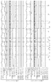
Next, the circuit operation of FIGS. 1 to 4 will be described together with the timing charts (time charts) of FIGS. In this description, the in-device synchronous clock source switching is
[0055]
[0056]
In the
[0057]
A frequency divider N301 in the digital PLL circuit 106 (FIG. 3) divides the
[0058]
The
[0059]
The
[0060]
The selection circuit T308 sends the
[0061]
The frequency divider P312 generates an output FP407 obtained by dividing the
[0062]
One
[0063]
Here, the
[0064]
The
[0065]
On the other hand,
[0066]
[0067]
[0068]
Second Embodiment: Next, a second embodiment of the present invention will be described in detail with reference to the drawings. FIG. 7 is a second embodiment of the present invention, and FIG. 8 is a timing chart.
[0069]
[0070]
On the other hand, the
[0071]
【The invention's effect】
The first effect is that a transmission signal can be transmitted without error even if the in-device clock synchronization source switching between the input interface units occurs. The reason is that the clock switching device according to the present invention makes the internal clock identical by supplying the clock and FP generated by the digital PLL circuit of the input interface unit selected as the internal clock synchronization source to the other input interface unit. By controlling the FP generated by another digital PLL circuit to have a unique phase relationship, the output phase from the plurality of input interface units to the phase control unit is kept constant. As a result, even if clock switching occurs, the FP of the input interface unit can be kept within the phase absorption range of the phase absorption circuit in the phase control unit, so that switching can be performed without generating a transmission signal error due to clock switching. Can do. For this reason, it becomes possible to transmit a transmission signal without error.
[0072]
The second effect is that an unnecessary alarm does not occur. The reason is that, conventionally, an out-of-synchronization alarm or the like is generated in the multiplexing circuit due to switching of the clock in the apparatus, but if the present invention is used, an out-of-synchronization does not occur and an unnecessary alarm does not occur.
[Brief description of the drawings]
FIG. 1 shows the configuration of a radio transmission apparatus having an active N line according to the present invention.
FIG. 2 is an input interface unit according to the first embodiment of the present invention.
FIG. 3 is a digital PLL circuit in the input interface unit of the present invention.
FIG. 4 is a phase controller of the present invention.
FIG. 5 is a clock synchronization circuit operation timing chart in the steady state of the present invention.
FIG. 6 is a clock synchronization circuit operation timing chart during the clock switching operation in the device of the present invention.
FIG. 7 shows an input interface unit according to a second embodiment of the present invention.
FIG. 8 is an operation timing chart of the clock synchronization circuit at the time of the internal clock switching operation according to the second embodiment of the present invention.
FIG. 9 shows an input interface unit according to a conventional example.
FIG. 10 is a digital PLL circuit in an input interface unit according to a conventional example.
FIG. 11 is an operation timing chart of a clock synchronization circuit in a steady state according to a conventional example.
FIG. 12 is an operation timing chart of the clock synchronization circuit at the time of the internal clock switching operation according to the conventional example.
[Explanation of symbols]
1 11 ~ 1 14 1 15 ~ 1 18 input signal
1 1 ~ 1 4 1 5 ~ 1 8 input signal
2 11 2 12 Input interface section
4 1 Phase controller
5 1 Modulator
6 1 Transmitter
7 1 Receiver
8 1 Demodulator
9 1 Distribution department
10 11 10 12 Output interface section
11 11 ~ 11 14 , 11 15 ~ 11 18 Output signal
101 Conversion circuit
102 Memory circuit
103 Multiplexing circuit
104 Extraction selection circuit
105 selection circuit
106 Digital PLL circuit
107 Voltage controlled transmitter
108 Phase absorption circuit
109 Selection circuit B
110 PLL circuit
111 Clock control circuit
112 Clock switching circuit
113 Subordinate control circuit
201 Input signal
209 output
210 Extracted clock information
211-214 Unipolar signal
219, 220 Extraction selection clock
221 Control signal
222 Selection output
223 Digital PLL output
224 Control output
225 Control output
226 Control output
227 Control output
228 control signal
229 Digital PLL output
301 Divider N
302 Divider M
303 Phase comparison circuit
304 transmitter
305 Timing generation circuit
306 A / D conversion circuit
307 Phase memory circuit
308 Selection circuit T
309 D / A conversion circuit
310 Loop filter
311 Voltage controlled transmitter
312 Divider P
401 N frequency division output
402 M frequency division output
403 Phase comparison result
404 count value
405 Memory value
406 output clock
407 output FP
408 Control signal
409 Comparison results
410 Control signal
Claims (3)
前記第1の入力インタフェース部への複数の入力信号からの一つを第1の同期クロック源として選択し、第1の抽出選択クロックとして送出する工程と、
前記第2の入力インタフェース部への複数の入力信号からの一つを第2の同期クロック源として選択し、第2の抽出選択クロックとして送出する工程と、
第1の選択回路において、前記第1の抽出選択クロックおよび前記第2の抽出選択クロックのいずれかを選択して第1の選択出力として送出する工程と、
第2の選択回路において、前記第1の抽出選択クロックおよび前記第2の抽出選択クロックのいずれかを選択して第2の選択出力として送出する工程と、
第1のディジタルPLL回路において、前記第1の選択出力に同期した、第1の同期クロックと第1の同期フレームパルス(FP)の生成を行い、前記第1の入力インタフェース部及び前記第2の入力インタフェース部に送出する工程と、
第2のディジタルPLL回路において、前記第2の選択出力に同期した、第2の同期クロックと第2の同期FPの生成を行い、前記第1の入力インタフェース部及び前記第2の入力インタフェース部に送出する工程と、
前記第1の入力インタフェース部において、前記第1の同期クロックおよび第1の同期FP、又は前記第2の同期クロックおよび第2の同期FP、のいずれかを選択して送出する工程と、
前記第2の入力インタフェース部において、前記第1の同期クロックおよび第1の同期FP、又は前記第2の同期クロックおよび第2の同期FP、のいずれかを選択して送出する工程と、
前記第1の同期FPの位相と前記第2の同期FPの位相が同じになるように制御する第1の制御出力を生成して、前記第1のディジタルPLL回路に送出する工程と、
前記第1の同期FPの位相と前記第2の同期FPの位相が同じになるように制御する第2の制御出力を生成して、前記第2のディジタルPLL回路に送出する工程と、を備えることを特徴とするクロック切替方法。A clock switching method for switching a clock from a first input interface unit to a second input interface unit in a transmission apparatus,
Selecting one of a plurality of input signals to the first input interface unit as a first synchronous clock source and sending it as a first extraction selection clock;
Selecting one of a plurality of input signals to the second input interface unit as a second synchronous clock source and sending it as a second extraction selection clock;
In the first selection circuit, selecting one of the first extraction selection clock and the second extraction selection clock and sending it as a first selection output;
In the second selection circuit, selecting either the first extraction selection clock or the second extraction selection clock and sending it as a second selection output;
In the first digital PLL circuit, a first synchronization clock and a first synchronization frame pulse (FP) are generated in synchronization with the first selection output, and the first input interface unit and the second synchronization frame pulse (FP) are generated. Sending to the input interface unit;
In the second digital PLL circuit, a second synchronous clock and a second synchronous FP that are synchronized with the second selected output are generated, and the first input interface unit and the second input interface unit A sending process;
Selecting and transmitting either the first synchronous clock and the first synchronous FP, or the second synchronous clock and the second synchronous FP in the first input interface unit;
Selecting and sending either the first synchronous clock and the first synchronous FP or the second synchronous clock and the second synchronous FP in the second input interface unit;
A step of the first synchronization FP phase and the second synchronization FP phases to generate a first control output for controlling to be the same, and sends it to the first digital PLL circuit,
Said first synchronization FP phase and the second synchronization FP phase generates a second control output for controlling to be the same, and a step of sending to said second digital PLL circuit And a clock switching method.
前記第1のインタフェース部は、第1の抽出選択回路と、第1の選択回路と、第1のディジタルPLL回路と、第1のクロック切替回路と、第1の従属制御回路とを備え、
前記第2のインタフェース部は、第2の抽出選択回路と、第2の選択回路と、第2のディジタルPLL回路と、第2のクロック切替回路と、第2の従属制御回路とを備え、
前記第1の抽出選択回路は、前記第1の入力インタフェース部への複数の入力信号からの一つを第1の同期クロック源として選択し、第1の抽出選択クロックとして前記第1の選択回路および前記第2の選択回路へ送出し、
前記第2の抽出選択回路は、前記第2の入力インタフェース部への複数の入力信号からの一つを第2の同期クロック源として選択し、第2の抽出選択クロックとして前記第1の選択回路および前記第2の選択回路へ送出し、
前記第1の選択回路は、前記第1の抽出選択クロックおよび前記第2の抽出選択クロックのいずれかを選択して第1の選択出力として前記第1のディジタルPLL回路へ送出し、
前記第2の選択回路は、前記第1の抽出選択クロックおよび前記第2の抽出選択クロックのいずれかを選択して第2の選択出力として前記第2のディジタルPLL回路へ送出し、
前記第1のディジタルPLL回路は、前記第1の選択出力に同期した、第1の同期クロックと第1の同期FPの生成を行い、前記第1の入力インタフェース部及び前記第2の入力インタフェース部に送出し、
前記第2のディジタルPLL回路は、前記第2の選択出力に同期した、第2の同期クロックと第2の同期FPの生成を行い、前記第1のクロック切替回路および前記第2のクロック切替回路へ送出し、
前記第1のクロック切替回路は、前記第1の同期クロックおよび第1の同期FP、又は前記第2の同期クロックおよび第2の同期FP、のいずれかを選択して送出し、
前記第2のクロック切替回路は、前記第1の同期クロックおよび第1の同期FP、又は前記第2の同期クロックおよび第2の同期FP、のいずれかを選択して送出し、
前記第1の従属制御回路は、前記第1の同期FPの位相と前記第2の同期FPの位相が同じになるように制御する第1の制御出力を生成して、前記第1のディジタルPLL回路に送出し、
前記第2の従属制御回路は、前記第1の同期FPの位相と前記第2の同期FPの位相が同じになるように制御する第2の制御出力を生成して、前記第2のディジタルPLL回路に送出する、
ことを特徴とするクロック切替装置。A clock switching device for switching a clock from a first input interface unit to a second input interface unit in a transmission device,
The first interface unit includes a first extraction selection circuit, a first selection circuit, a first digital PLL circuit, a first clock switching circuit, and a first subordinate control circuit,
The second interface unit includes a second extraction selection circuit, a second selection circuit, a second digital PLL circuit, a second clock switching circuit, and a second subordinate control circuit,
The first extraction selection circuit selects one of a plurality of input signals to the first input interface unit as a first synchronous clock source, and uses the first selection circuit as a first extraction selection clock. And sending to the second selection circuit,
The second extraction selection circuit selects one of a plurality of input signals to the second input interface unit as a second synchronous clock source, and uses the first selection circuit as a second extraction selection clock. And sending to the second selection circuit,
The first selection circuit selects one of the first extraction selection clock and the second extraction selection clock and sends it to the first digital PLL circuit as a first selection output;
The second selection circuit selects either the first extraction selection clock or the second extraction selection clock and sends it to the second digital PLL circuit as a second selection output;
The first digital PLL circuit generates a first synchronous clock and a first synchronous FP synchronized with the first selection output, and the first input interface unit and the second input interface unit To
The second digital PLL circuit generates a second synchronous clock and a second synchronous FP synchronized with the second selection output, and the first clock switching circuit and the second clock switching circuit To
The first clock switching circuit selects and sends either the first synchronous clock and the first synchronous FP, or the second synchronous clock and the second synchronous FP,
The second clock switching circuit selects and sends either the first synchronous clock and the first synchronous FP, or the second synchronous clock and the second synchronous FP,
The first dependent control circuit, said first first generates a control output, wherein the synchronized FP phase second synchronization FP phase is controlled to be the same, the first digital PLL To the circuit,
It said second slave control circuit, the first second and generates a control output, wherein the synchronized FP phase second synchronization FP phase is controlled to be the same, the second digital PLL Send to circuit,
A clock switching device.
前記選択回路の選択出力をN(N≧2)分周したN分周出力を送出する分周器Nと、
前記クロックをM(M≧2)分周したM分周出力を送出する分周器Mと、
前記N分周出力及び前記M分周出力の位相比較を行い、位相比較結果を送出する位相比較回路と、
前記位相比較結果をカウントし、カウント値を送出するA/D変換回路と、
前記カウント値を記憶し記憶値として送出する位相記憶回路と、
前記カウント値及び前記記憶値の選択出力を選択値として送出する選択回路Tと、
前記選択値をD/A変換してアナログ電圧を生成して送出するD/A変換回路と、
前記アナログ電圧に含まれる不要な周波数成分を抑圧して送出するループフィルタと、
前記ループフィルタから送出された電圧に従って周波数を制御した前記クロックを送出する電圧制御発信器と、
前記クロックをP(P≧2)分周して生成したFPを送出する分周器Pと、
前記カウント値と前記記憶値の比較を行い比較結果を送出する比較回路と、
前記選択回路T、前記位相記憶回路、前記分周器Mを制御する制御回路と、
を備えることを特徴とする請求項2に記載のクロック切替装置。The first and second digital PLL circuits are
A frequency divider N for transmitting an N-divided output obtained by dividing the selection output of the selection circuit by N (N ≧ 2);
A frequency divider M for transmitting an M-divided output obtained by dividing the clock by M (M ≧ 2);
A phase comparison circuit that performs phase comparison of the N-divided output and the M-divided output and sends out a phase comparison result;
An A / D conversion circuit that counts the phase comparison results and sends a count value;
A phase storage circuit for storing the count value and sending it as a stored value;
A selection circuit T for sending a selection output of the count value and the stored value as a selection value;
A D / A conversion circuit for D / A converting the selected value to generate and send an analog voltage;
A loop filter that suppresses and transmits unnecessary frequency components included in the analog voltage;
A voltage controlled oscillator for transmitting the clock whose frequency is controlled according to the voltage transmitted from the loop filter;
A frequency divider P for sending out an FP generated by dividing the clock by P (P ≧ 2);
A comparison circuit that compares the count value with the stored value and sends a comparison result;
A control circuit for controlling the selection circuit T, the phase storage circuit, and the frequency divider M;
The clock switching device according to claim 2, further comprising:
Priority Applications (1)
| Application Number | Priority Date | Filing Date | Title |
|---|---|---|---|
| JP2002342362A JP4336790B2 (en) | 2002-11-26 | 2002-11-26 | Clock switching method and clock switching device |
Applications Claiming Priority (1)
| Application Number | Priority Date | Filing Date | Title |
|---|---|---|---|
| JP2002342362A JP4336790B2 (en) | 2002-11-26 | 2002-11-26 | Clock switching method and clock switching device |
Publications (2)
| Publication Number | Publication Date |
|---|---|
| JP2004179864A JP2004179864A (en) | 2004-06-24 |
| JP4336790B2 true JP4336790B2 (en) | 2009-09-30 |
Family
ID=32704452
Family Applications (1)
| Application Number | Title | Priority Date | Filing Date |
|---|---|---|---|
| JP2002342362A Expired - Fee Related JP4336790B2 (en) | 2002-11-26 | 2002-11-26 | Clock switching method and clock switching device |
Country Status (1)
| Country | Link |
|---|---|
| JP (1) | JP4336790B2 (en) |
Families Citing this family (1)
| Publication number | Priority date | Publication date | Assignee | Title |
|---|---|---|---|---|
| CN114108236A (en) * | 2020-08-31 | 2022-03-01 | 天津海尔洗涤电器有限公司 | Dewatering control method and device for washing equipment |
-
2002
- 2002-11-26 JP JP2002342362A patent/JP4336790B2/en not_active Expired - Fee Related
Also Published As
| Publication number | Publication date |
|---|---|
| JP2004179864A (en) | 2004-06-24 |
Similar Documents
| Publication | Publication Date | Title |
|---|---|---|
| JP2012049754A (en) | Clock generation circuit | |
| JP3850063B2 (en) | Method and apparatus for determining feedback division ratio in a phase locked loop | |
| JP4336790B2 (en) | Clock switching method and clock switching device | |
| US9832551B2 (en) | Optical transmission device and optical transmission control method | |
| JP4183535B2 (en) | Optical signal transmission device for speed conversion processing of frame signal | |
| JP4156529B2 (en) | Selectable clocking architecture | |
| KR100328757B1 (en) | A error preventing device of clock signal with switchover for transmission system | |
| JP7083644B2 (en) | Clock switching device | |
| US5923704A (en) | Transmit clock generation system and method | |
| JP7198335B2 (en) | clock switching device | |
| JPH07273648A (en) | Pll circuit | |
| US20070079163A1 (en) | Transmitting apparatus | |
| JP4465658B2 (en) | Clock converter, modulator, and transmitter for digital broadcasting | |
| JP3655878B2 (en) | PLL circuit | |
| JP2015171002A (en) | Electric/electronic apparatus, circuit and communication system | |
| KR20000061197A (en) | Apparatus and method for controlling clock frequency using plural phase-locked loops | |
| KR100560434B1 (en) | Apparatus for providing system clock synchronized to network universally | |
| JP2004201119A (en) | Relay transmission device, relay transmission method, and relay transmission program | |
| KR100257344B1 (en) | Digital pll circuit | |
| JP3720552B2 (en) | Dual clock synchronous control system | |
| JP2009212659A (en) | Phase difference correction circuit and phase difference correction method | |
| JP4089352B2 (en) | Frame pulse switching circuit and phase control method thereof | |
| JPH11298460A (en) | Clock changeover circuit | |
| KR100328761B1 (en) | A device of switching system clock unit for optical communication system | |
| JP2972463B2 (en) | Synchronous signal supply device |
Legal Events
| Date | Code | Title | Description |
|---|---|---|---|
| RD01 | Notification of change of attorney |
Free format text: JAPANESE INTERMEDIATE CODE: A7421 Effective date: 20050309 |
|
| A621 | Written request for application examination |
Free format text: JAPANESE INTERMEDIATE CODE: A621 Effective date: 20051017 |
|
| RD01 | Notification of change of attorney |
Free format text: JAPANESE INTERMEDIATE CODE: A7421 Effective date: 20070118 |
|
| A977 | Report on retrieval |
Free format text: JAPANESE INTERMEDIATE CODE: A971007 Effective date: 20071107 |
|
| A131 | Notification of reasons for refusal |
Free format text: JAPANESE INTERMEDIATE CODE: A131 Effective date: 20071113 |
|
| A521 | Written amendment |
Free format text: JAPANESE INTERMEDIATE CODE: A523 Effective date: 20080111 |
|
| RD01 | Notification of change of attorney |
Free format text: JAPANESE INTERMEDIATE CODE: A7421 Effective date: 20080610 |
|
| A131 | Notification of reasons for refusal |
Free format text: JAPANESE INTERMEDIATE CODE: A131 Effective date: 20080930 |
|
| A521 | Written amendment |
Free format text: JAPANESE INTERMEDIATE CODE: A523 Effective date: 20081201 |
|
| RD01 | Notification of change of attorney |
Free format text: JAPANESE INTERMEDIATE CODE: A7421 Effective date: 20090508 |
|
| TRDD | Decision of grant or rejection written | ||
| A01 | Written decision to grant a patent or to grant a registration (utility model) |
Free format text: JAPANESE INTERMEDIATE CODE: A01 Effective date: 20090526 |
|
| A01 | Written decision to grant a patent or to grant a registration (utility model) |
Free format text: JAPANESE INTERMEDIATE CODE: A01 |
|
| A61 | First payment of annual fees (during grant procedure) |
Free format text: JAPANESE INTERMEDIATE CODE: A61 Effective date: 20090608 |
|
| R150 | Certificate of patent or registration of utility model |
Free format text: JAPANESE INTERMEDIATE CODE: R150 |
|
| FPAY | Renewal fee payment (event date is renewal date of database) |
Free format text: PAYMENT UNTIL: 20120710 Year of fee payment: 3 |
|
| FPAY | Renewal fee payment (event date is renewal date of database) |
Free format text: PAYMENT UNTIL: 20120710 Year of fee payment: 3 |
|
| FPAY | Renewal fee payment (event date is renewal date of database) |
Free format text: PAYMENT UNTIL: 20130710 Year of fee payment: 4 |
|
| LAPS | Cancellation because of no payment of annual fees |