JP4338298B2 - 電荷転送装置およびその駆動方法 - Google Patents
電荷転送装置およびその駆動方法 Download PDFInfo
- Publication number
- JP4338298B2 JP4338298B2 JP2000304290A JP2000304290A JP4338298B2 JP 4338298 B2 JP4338298 B2 JP 4338298B2 JP 2000304290 A JP2000304290 A JP 2000304290A JP 2000304290 A JP2000304290 A JP 2000304290A JP 4338298 B2 JP4338298 B2 JP 4338298B2
- Authority
- JP
- Japan
- Prior art keywords
- charge transfer
- region
- horizontal
- vertical
- charges
- Prior art date
- Legal status (The legal status is an assumption and is not a legal conclusion. Google has not performed a legal analysis and makes no representation as to the accuracy of the status listed.)
- Expired - Fee Related
Links
Images







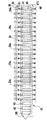

Classifications
-
- H—ELECTRICITY
- H04—ELECTRIC COMMUNICATION TECHNIQUE
- H04N—PICTORIAL COMMUNICATION, e.g. TELEVISION
- H04N25/00—Circuitry of solid-state image sensors [SSIS]; Control thereof
- H04N25/10—Circuitry of solid-state image sensors [SSIS]; Control thereof for transforming different wavelengths into image signals
- H04N25/11—Arrangement of colour filter arrays [CFA]; Filter mosaics
- H04N25/13—Arrangement of colour filter arrays [CFA]; Filter mosaics characterised by the spectral characteristics of the filter elements
- H04N25/135—Arrangement of colour filter arrays [CFA]; Filter mosaics characterised by the spectral characteristics of the filter elements based on four or more different wavelength filter elements
-
- H—ELECTRICITY
- H10—SEMICONDUCTOR DEVICES; ELECTRIC SOLID-STATE DEVICES NOT OTHERWISE PROVIDED FOR
- H10F—INORGANIC SEMICONDUCTOR DEVICES SENSITIVE TO INFRARED RADIATION, LIGHT, ELECTROMAGNETIC RADIATION OF SHORTER WAVELENGTH OR CORPUSCULAR RADIATION
- H10F39/00—Integrated devices, or assemblies of multiple devices, comprising at least one element covered by group H10F30/00, e.g. radiation detectors comprising photodiode arrays
- H10F39/10—Integrated devices
- H10F39/12—Image sensors
- H10F39/15—Charge-coupled device [CCD] image sensors
- H10F39/153—Two-dimensional or three-dimensional array CCD image sensors
-
- H—ELECTRICITY
- H10—SEMICONDUCTOR DEVICES; ELECTRIC SOLID-STATE DEVICES NOT OTHERWISE PROVIDED FOR
- H10F—INORGANIC SEMICONDUCTOR DEVICES SENSITIVE TO INFRARED RADIATION, LIGHT, ELECTROMAGNETIC RADIATION OF SHORTER WAVELENGTH OR CORPUSCULAR RADIATION
- H10F39/00—Integrated devices, or assemblies of multiple devices, comprising at least one element covered by group H10F30/00, e.g. radiation detectors comprising photodiode arrays
- H10F39/10—Integrated devices
- H10F39/12—Image sensors
- H10F39/15—Charge-coupled device [CCD] image sensors
- H10F39/156—CCD or CID colour image sensors
-
- H—ELECTRICITY
- H10—SEMICONDUCTOR DEVICES; ELECTRIC SOLID-STATE DEVICES NOT OTHERWISE PROVIDED FOR
- H10F—INORGANIC SEMICONDUCTOR DEVICES SENSITIVE TO INFRARED RADIATION, LIGHT, ELECTROMAGNETIC RADIATION OF SHORTER WAVELENGTH OR CORPUSCULAR RADIATION
- H10F39/00—Integrated devices, or assemblies of multiple devices, comprising at least one element covered by group H10F30/00, e.g. radiation detectors comprising photodiode arrays
- H10F39/80—Constructional details of image sensors
Landscapes
- Physics & Mathematics (AREA)
- Spectroscopy & Molecular Physics (AREA)
- Engineering & Computer Science (AREA)
- Multimedia (AREA)
- Signal Processing (AREA)
- Solid State Image Pick-Up Elements (AREA)
- Transforming Light Signals Into Electric Signals (AREA)
Priority Applications (4)
| Application Number | Priority Date | Filing Date | Title |
|---|---|---|---|
| JP2000304290A JP4338298B2 (ja) | 2000-10-04 | 2000-10-04 | 電荷転送装置およびその駆動方法 |
| US09/968,995 US7187411B2 (en) | 2000-10-04 | 2001-10-03 | Charge transfer device having discharge drain, CCD image sensor, and CCD image pickup system |
| DE60128991T DE60128991T2 (de) | 2000-10-04 | 2001-10-04 | Ladungsübertragungsvorrichtung und Ansteuerungsverfahren dazu |
| EP01123776A EP1195986B1 (fr) | 2000-10-04 | 2001-10-04 | Dispositif à transfert de charges et procédé pour le commander |
Applications Claiming Priority (1)
| Application Number | Priority Date | Filing Date | Title |
|---|---|---|---|
| JP2000304290A JP4338298B2 (ja) | 2000-10-04 | 2000-10-04 | 電荷転送装置およびその駆動方法 |
Publications (2)
| Publication Number | Publication Date |
|---|---|
| JP2002112122A JP2002112122A (ja) | 2002-04-12 |
| JP4338298B2 true JP4338298B2 (ja) | 2009-10-07 |
Family
ID=18785359
Family Applications (1)
| Application Number | Title | Priority Date | Filing Date |
|---|---|---|---|
| JP2000304290A Expired - Fee Related JP4338298B2 (ja) | 2000-10-04 | 2000-10-04 | 電荷転送装置およびその駆動方法 |
Country Status (4)
| Country | Link |
|---|---|
| US (1) | US7187411B2 (fr) |
| EP (1) | EP1195986B1 (fr) |
| JP (1) | JP4338298B2 (fr) |
| DE (1) | DE60128991T2 (fr) |
Families Citing this family (30)
| Publication number | Priority date | Publication date | Assignee | Title |
|---|---|---|---|---|
| JP4341177B2 (ja) * | 2000-12-15 | 2009-10-07 | ソニー株式会社 | 固体撮像装置およびその駆動方法、並びに画像読取装置 |
| US7292277B2 (en) * | 2002-04-08 | 2007-11-06 | Fujifilm Corporation | Solid-state image pick-up device and digital still camera |
| JP2004140258A (ja) * | 2002-10-18 | 2004-05-13 | Sanyo Electric Co Ltd | 固体撮像素子及びその製造方法 |
| JP2004172846A (ja) * | 2002-11-19 | 2004-06-17 | Canon Inc | 固体撮像装置 |
| FR2855326B1 (fr) * | 2003-05-23 | 2005-07-22 | Atmel Grenoble Sa | Capteur d'image matriciel en technologie cmos |
| JP4658470B2 (ja) * | 2003-11-28 | 2011-03-23 | パナソニック株式会社 | 固体撮像素子、固体撮像装置及びカメラ |
| JP2005167665A (ja) * | 2003-12-03 | 2005-06-23 | Sanyo Electric Co Ltd | 画像信号処理装置、画像信号処理方法、画像信号処理プログラム、固体撮像素子の制御装置及び固体撮像素子の制御方法 |
| JP4782989B2 (ja) * | 2004-05-10 | 2011-09-28 | パナソニック株式会社 | 固体撮像装置 |
| US20050254817A1 (en) * | 2004-05-13 | 2005-11-17 | Mckee William J | Autostereoscopic electronic camera |
| JP2006157624A (ja) * | 2004-11-30 | 2006-06-15 | Fuji Film Microdevices Co Ltd | 固体撮像装置及び固体撮像装置の駆動方法 |
| JP4457961B2 (ja) | 2005-04-28 | 2010-04-28 | ソニー株式会社 | 固体撮像素子 |
| JP4907941B2 (ja) * | 2005-09-29 | 2012-04-04 | ルネサスエレクトロニクス株式会社 | 固体撮像装置およびその駆動方法 |
| JP4763424B2 (ja) | 2005-11-08 | 2011-08-31 | 富士フイルム株式会社 | 固体撮像素子の駆動方法 |
| TWI370678B (en) * | 2006-02-15 | 2012-08-11 | Sony Corp | Solid-state image-capturing device, driving method thereof, camera, electric charge transfer device, driving method and driving device for driving load, and electronic equipment |
| JP4992446B2 (ja) * | 2006-02-24 | 2012-08-08 | ソニー株式会社 | 固体撮像装置及びその製造方法、並びにカメラ |
| JP2007295230A (ja) * | 2006-04-25 | 2007-11-08 | Matsushita Electric Ind Co Ltd | 固体撮像装置およびその駆動方法、カメラ |
| US20070291165A1 (en) * | 2006-06-20 | 2007-12-20 | Ming-Yan Wang | Hands-free portable digital video camera device |
| JP2008028646A (ja) * | 2006-07-20 | 2008-02-07 | Fujifilm Corp | Ccd型固体撮像装置及びその駆動方法 |
| JP2008042629A (ja) | 2006-08-08 | 2008-02-21 | Fujifilm Corp | 固体撮像素子の駆動方法 |
| WO2008066067A1 (fr) * | 2006-11-28 | 2008-06-05 | Hamamatsu Photonics K.K. | Élément d'imagerie à l'état solide |
| US20100165166A1 (en) * | 2007-06-08 | 2010-07-01 | Panasonic Corporation | Solid-state imaging device |
| US7965331B2 (en) * | 2007-07-23 | 2011-06-21 | Fujifilm Corporation | Solid state imaging element, image pickup device and method of driving solid state imaging element |
| JP2009089029A (ja) * | 2007-09-28 | 2009-04-23 | Fujifilm Corp | Ccd型固体撮像素子 |
| KR101435877B1 (ko) * | 2007-12-13 | 2014-09-02 | 삼성전자주식회사 | 디지털 촬영장치 및 촬상소자 구동방법 |
| US8134630B2 (en) * | 2008-05-09 | 2012-03-13 | Truesense Imaging, Inc. | System and method for draining residual charge from charge-coupled device (CCD) shift registers in image sensors having reset drains |
| US20100194673A1 (en) * | 2009-02-05 | 2010-08-05 | Nokia Corporation | Device and a method for an image sensor and a method for manufacturing an image sensor |
| JP5473951B2 (ja) | 2009-02-13 | 2014-04-16 | パナソニック株式会社 | 固体撮像装置及びカメラ |
| KR101167159B1 (ko) * | 2011-04-22 | 2012-07-24 | (주)세미솔루션 | 씨씨디 카메라용 센서 통합 칩 |
| JP6700673B2 (ja) * | 2015-05-15 | 2020-05-27 | キヤノン株式会社 | 撮像装置、撮像システム |
| DE102017003170A1 (de) * | 2017-03-31 | 2018-10-04 | MAX-PLANCK-Gesellschaft zur Förderung der Wissenschaften e.V. | Verfahren und Vorrichtung zur Korrektur von Smear-Artefakten |
Family Cites Families (13)
| Publication number | Priority date | Publication date | Assignee | Title |
|---|---|---|---|---|
| EP0621726B1 (fr) * | 1993-04-20 | 1999-06-16 | Sony Corporation | Méthode et appareillage pour un dispositif d'imagerie à l'état solide |
| JPH07161958A (ja) | 1993-12-09 | 1995-06-23 | Nec Corp | 固体撮像装置 |
| JP2699841B2 (ja) * | 1993-12-10 | 1998-01-19 | 日本電気株式会社 | 固体撮像装置 |
| JP3318814B2 (ja) | 1995-03-15 | 2002-08-26 | ソニー株式会社 | 固体撮像装置及びその駆動方法 |
| JP3715353B2 (ja) | 1995-09-01 | 2005-11-09 | ソニー株式会社 | 固体撮像素子 |
| JP4329128B2 (ja) * | 1996-07-12 | 2009-09-09 | ソニー株式会社 | 固体撮像装置、固体撮像装置の駆動方法およびカメラ |
| JP2845216B2 (ja) * | 1996-09-27 | 1999-01-13 | 日本電気株式会社 | 固体撮像装置およびその製造方法 |
| US6707498B1 (en) * | 1997-11-11 | 2004-03-16 | Fuji Photo Film Co., Ltd. | Charge transfer of solid-state image pickup device |
| JP4020488B2 (ja) * | 1998-05-18 | 2007-12-12 | 富士フイルム株式会社 | 固体撮像装置 |
| JP2000106678A (ja) * | 1998-09-28 | 2000-04-11 | Victor Co Of Japan Ltd | 撮像装置 |
| JP2000152093A (ja) | 1998-11-12 | 2000-05-30 | Sony Corp | 固体撮像素子 |
| JP4199387B2 (ja) | 1999-10-07 | 2008-12-17 | 富士フイルム株式会社 | 電荷転送路およびそれを用いた固体撮像装置 |
| JP4515617B2 (ja) * | 2000-10-23 | 2010-08-04 | 富士フイルム株式会社 | 固体撮像素子およびその駆動方法 |
-
2000
- 2000-10-04 JP JP2000304290A patent/JP4338298B2/ja not_active Expired - Fee Related
-
2001
- 2001-10-03 US US09/968,995 patent/US7187411B2/en not_active Expired - Fee Related
- 2001-10-04 DE DE60128991T patent/DE60128991T2/de not_active Expired - Lifetime
- 2001-10-04 EP EP01123776A patent/EP1195986B1/fr not_active Expired - Lifetime
Also Published As
| Publication number | Publication date |
|---|---|
| DE60128991T2 (de) | 2007-10-18 |
| US20020039144A1 (en) | 2002-04-04 |
| EP1195986A2 (fr) | 2002-04-10 |
| EP1195986A3 (fr) | 2004-04-21 |
| EP1195986B1 (fr) | 2007-06-20 |
| JP2002112122A (ja) | 2002-04-12 |
| DE60128991D1 (de) | 2007-08-02 |
| US7187411B2 (en) | 2007-03-06 |
Similar Documents
| Publication | Publication Date | Title |
|---|---|---|
| JP4338298B2 (ja) | 電荷転送装置およびその駆動方法 | |
| JP4515617B2 (ja) | 固体撮像素子およびその駆動方法 | |
| JP4497688B2 (ja) | 固体撮像装置 | |
| US6885399B1 (en) | Solid state imaging device configured to add separated signal charges | |
| JP4423452B2 (ja) | 固体撮像装置 | |
| JP4139088B2 (ja) | 固体撮像装置及びその制御方法 | |
| US6541805B1 (en) | Solid-state image pickup device | |
| JP4497261B2 (ja) | 電荷転送装置、ccdイメージセンサおよびccd撮像システム | |
| US6822682B1 (en) | Solid state image pickup device and its read method | |
| JP4252685B2 (ja) | 固体撮像装置 | |
| KR100433770B1 (ko) | 고체 촬상 소자 및 그 구동 방법 | |
| JP4514912B2 (ja) | 固体撮像装置およびその駆動方法 | |
| JP2005229503A (ja) | 固体撮像装置 | |
| JP2002185870A (ja) | 固体撮像素子 | |
| JP4132003B2 (ja) | 固体撮像装置 | |
| JP3795808B2 (ja) | 固体撮像素子およびこれを用いた撮像装置 | |
| JP3750221B2 (ja) | 固体撮像装置 | |
| JP4514208B2 (ja) | 固体撮像装置およびその駆動方法 | |
| JP2978018B2 (ja) | 固体撮像装置とその駆動方法 | |
| JP4010446B2 (ja) | 電荷転送装置および固体撮像素子 | |
| JP2003060185A (ja) | 固体撮像装置及びその制御方法 | |
| JP4249349B2 (ja) | 固体撮像装置 | |
| JP2002335450A (ja) | 固体撮像素子の駆動方法および固体撮像素子 | |
| JP2002064833A (ja) | 固体撮像素子および固体撮像装置 | |
| JP2001244451A (ja) | 固体撮像装置 |
Legal Events
| Date | Code | Title | Description |
|---|---|---|---|
| A711 | Notification of change in applicant |
Free format text: JAPANESE INTERMEDIATE CODE: A712 Effective date: 20060621 |
|
| A711 | Notification of change in applicant |
Free format text: JAPANESE INTERMEDIATE CODE: A712 Effective date: 20061213 |
|
| A521 | Request for written amendment filed |
Free format text: JAPANESE INTERMEDIATE CODE: A523 Effective date: 20061221 |
|
| A521 | Request for written amendment filed |
Free format text: JAPANESE INTERMEDIATE CODE: A523 Effective date: 20070216 |
|
| A621 | Written request for application examination |
Free format text: JAPANESE INTERMEDIATE CODE: A621 Effective date: 20070521 |
|
| A131 | Notification of reasons for refusal |
Free format text: JAPANESE INTERMEDIATE CODE: A131 Effective date: 20081028 |
|
| A521 | Request for written amendment filed |
Free format text: JAPANESE INTERMEDIATE CODE: A523 Effective date: 20090105 |
|
| A131 | Notification of reasons for refusal |
Free format text: JAPANESE INTERMEDIATE CODE: A131 Effective date: 20090203 |
|
| A521 | Request for written amendment filed |
Free format text: JAPANESE INTERMEDIATE CODE: A523 Effective date: 20090331 |
|
| TRDD | Decision of grant or rejection written | ||
| A01 | Written decision to grant a patent or to grant a registration (utility model) |
Free format text: JAPANESE INTERMEDIATE CODE: A01 Effective date: 20090623 |
|
| A01 | Written decision to grant a patent or to grant a registration (utility model) |
Free format text: JAPANESE INTERMEDIATE CODE: A01 |
|
| A61 | First payment of annual fees (during grant procedure) |
Free format text: JAPANESE INTERMEDIATE CODE: A61 Effective date: 20090630 |
|
| R150 | Certificate of patent or registration of utility model |
Free format text: JAPANESE INTERMEDIATE CODE: R150 |
|
| FPAY | Renewal fee payment (event date is renewal date of database) |
Free format text: PAYMENT UNTIL: 20120710 Year of fee payment: 3 |
|
| LAPS | Cancellation because of no payment of annual fees |