JP4338545B2 - コンデンサシート - Google Patents
コンデンサシート Download PDFInfo
- Publication number
- JP4338545B2 JP4338545B2 JP2004042877A JP2004042877A JP4338545B2 JP 4338545 B2 JP4338545 B2 JP 4338545B2 JP 2004042877 A JP2004042877 A JP 2004042877A JP 2004042877 A JP2004042877 A JP 2004042877A JP 4338545 B2 JP4338545 B2 JP 4338545B2
- Authority
- JP
- Japan
- Prior art keywords
- capacitor
- electrode
- block
- ground
- capacitor block
- Prior art date
- Legal status (The legal status is an assumption and is not a legal conclusion. Google has not performed a legal analysis and makes no representation as to the accuracy of the status listed.)
- Expired - Fee Related
Links
Images






Classifications
-
- H—ELECTRICITY
- H01—ELECTRIC ELEMENTS
- H01G—CAPACITORS; CAPACITORS, RECTIFIERS, DETECTORS, SWITCHING DEVICES, LIGHT-SENSITIVE OR TEMPERATURE-SENSITIVE DEVICES OF THE ELECTROLYTIC TYPE
- H01G4/00—Fixed capacitors; Processes of their manufacture
- H01G4/35—Feed-through capacitors or anti-noise capacitors
-
- H—ELECTRICITY
- H05—ELECTRIC TECHNIQUES NOT OTHERWISE PROVIDED FOR
- H05K—PRINTED CIRCUITS; CASINGS OR CONSTRUCTIONAL DETAILS OF ELECTRIC APPARATUS; MANUFACTURE OF ASSEMBLAGES OF ELECTRICAL COMPONENTS
- H05K1/00—Printed circuits
- H05K1/02—Details
- H05K1/0213—Electrical arrangements not otherwise provided for
- H05K1/0216—Reduction of cross-talk, noise or electromagnetic interference
- H05K1/023—Reduction of cross-talk, noise or electromagnetic interference using auxiliary mounted passive components or auxiliary substances
- H05K1/0231—Capacitors or dielectric substances
-
- H—ELECTRICITY
- H10—SEMICONDUCTOR DEVICES; ELECTRIC SOLID-STATE DEVICES NOT OTHERWISE PROVIDED FOR
- H10W—GENERIC PACKAGES, INTERCONNECTIONS, CONNECTORS OR OTHER CONSTRUCTIONAL DETAILS OF DEVICES COVERED BY CLASS H10
- H10W70/00—Package substrates; Interposers; Redistribution layers [RDL]
- H10W70/60—Insulating or insulated package substrates; Interposers; Redistribution layers
- H10W70/62—Insulating or insulated package substrates; Interposers; Redistribution layers characterised by their interconnections
- H10W70/63—Vias, e.g. via plugs
- H10W70/635—Through-vias
-
- H—ELECTRICITY
- H10—SEMICONDUCTOR DEVICES; ELECTRIC SOLID-STATE DEVICES NOT OTHERWISE PROVIDED FOR
- H10W—GENERIC PACKAGES, INTERCONNECTIONS, CONNECTORS OR OTHER CONSTRUCTIONAL DETAILS OF DEVICES COVERED BY CLASS H10
- H10W72/00—Interconnections or connectors in packages
-
- H—ELECTRICITY
- H05—ELECTRIC TECHNIQUES NOT OTHERWISE PROVIDED FOR
- H05K—PRINTED CIRCUITS; CASINGS OR CONSTRUCTIONAL DETAILS OF ELECTRIC APPARATUS; MANUFACTURE OF ASSEMBLAGES OF ELECTRICAL COMPONENTS
- H05K1/00—Printed circuits
- H05K1/02—Details
- H05K1/0213—Electrical arrangements not otherwise provided for
- H05K1/0216—Reduction of cross-talk, noise or electromagnetic interference
- H05K1/0218—Reduction of cross-talk, noise or electromagnetic interference by printed shielding conductors, ground planes or power plane
- H05K1/0219—Printed shielding conductors for shielding around or between signal conductors, e.g. coplanar or coaxial printed shielding conductors
-
- H—ELECTRICITY
- H05—ELECTRIC TECHNIQUES NOT OTHERWISE PROVIDED FOR
- H05K—PRINTED CIRCUITS; CASINGS OR CONSTRUCTIONAL DETAILS OF ELECTRIC APPARATUS; MANUFACTURE OF ASSEMBLAGES OF ELECTRICAL COMPONENTS
- H05K1/00—Printed circuits
- H05K1/16—Printed circuits incorporating printed electric components, e.g. printed resistors, capacitors or inductors
- H05K1/162—Printed circuits incorporating printed electric components, e.g. printed resistors, capacitors or inductors incorporating printed capacitors
-
- H—ELECTRICITY
- H05—ELECTRIC TECHNIQUES NOT OTHERWISE PROVIDED FOR
- H05K—PRINTED CIRCUITS; CASINGS OR CONSTRUCTIONAL DETAILS OF ELECTRIC APPARATUS; MANUFACTURE OF ASSEMBLAGES OF ELECTRICAL COMPONENTS
- H05K2201/00—Indexing scheme relating to printed circuits covered by H05K1/00
- H05K2201/10—Details of components or other objects attached to or integrated in a printed circuit board
- H05K2201/10227—Other objects, e.g. metallic pieces
- H05K2201/10378—Interposers
-
- H—ELECTRICITY
- H05—ELECTRIC TECHNIQUES NOT OTHERWISE PROVIDED FOR
- H05K—PRINTED CIRCUITS; CASINGS OR CONSTRUCTIONAL DETAILS OF ELECTRIC APPARATUS; MANUFACTURE OF ASSEMBLAGES OF ELECTRICAL COMPONENTS
- H05K2201/00—Indexing scheme relating to printed circuits covered by H05K1/00
- H05K2201/10—Details of components or other objects attached to or integrated in a printed circuit board
- H05K2201/10613—Details of electrical connections of non-printed components, e.g. special leads
- H05K2201/10621—Components characterised by their electrical contacts
- H05K2201/10734—Ball grid array [BGA]; Bump grid array
-
- H—ELECTRICITY
- H10—SEMICONDUCTOR DEVICES; ELECTRIC SOLID-STATE DEVICES NOT OTHERWISE PROVIDED FOR
- H10W—GENERIC PACKAGES, INTERCONNECTIONS, CONNECTORS OR OTHER CONSTRUCTIONAL DETAILS OF DEVICES COVERED BY CLASS H10
- H10W70/00—Package substrates; Interposers; Redistribution layers [RDL]
- H10W70/01—Manufacture or treatment
- H10W70/05—Manufacture or treatment of insulating or insulated package substrates, or of interposers, or of redistribution layers
- H10W70/093—Connecting or disconnecting other interconnections thereto or therefrom, e.g. connecting bond wires or bumps
-
- H—ELECTRICITY
- H10—SEMICONDUCTOR DEVICES; ELECTRIC SOLID-STATE DEVICES NOT OTHERWISE PROVIDED FOR
- H10W—GENERIC PACKAGES, INTERCONNECTIONS, CONNECTORS OR OTHER CONSTRUCTIONAL DETAILS OF DEVICES COVERED BY CLASS H10
- H10W72/00—Interconnections or connectors in packages
- H10W72/071—Connecting or disconnecting
- H10W72/072—Connecting or disconnecting of bump connectors
- H10W72/07231—Techniques
- H10W72/07236—Soldering or alloying
-
- H—ELECTRICITY
- H10—SEMICONDUCTOR DEVICES; ELECTRIC SOLID-STATE DEVICES NOT OTHERWISE PROVIDED FOR
- H10W—GENERIC PACKAGES, INTERCONNECTIONS, CONNECTORS OR OTHER CONSTRUCTIONAL DETAILS OF DEVICES COVERED BY CLASS H10
- H10W72/00—Interconnections or connectors in packages
- H10W72/071—Connecting or disconnecting
- H10W72/072—Connecting or disconnecting of bump connectors
- H10W72/07251—Connecting or disconnecting of bump connectors characterised by changes in properties of the bump connectors during connecting
-
- H—ELECTRICITY
- H10—SEMICONDUCTOR DEVICES; ELECTRIC SOLID-STATE DEVICES NOT OTHERWISE PROVIDED FOR
- H10W—GENERIC PACKAGES, INTERCONNECTIONS, CONNECTORS OR OTHER CONSTRUCTIONAL DETAILS OF DEVICES COVERED BY CLASS H10
- H10W72/00—Interconnections or connectors in packages
- H10W72/071—Connecting or disconnecting
- H10W72/075—Connecting or disconnecting of bond wires
-
- H—ELECTRICITY
- H10—SEMICONDUCTOR DEVICES; ELECTRIC SOLID-STATE DEVICES NOT OTHERWISE PROVIDED FOR
- H10W—GENERIC PACKAGES, INTERCONNECTIONS, CONNECTORS OR OTHER CONSTRUCTIONAL DETAILS OF DEVICES COVERED BY CLASS H10
- H10W72/00—Interconnections or connectors in packages
- H10W72/071—Connecting or disconnecting
- H10W72/077—Connecting of TAB connectors
-
- H—ELECTRICITY
- H10—SEMICONDUCTOR DEVICES; ELECTRIC SOLID-STATE DEVICES NOT OTHERWISE PROVIDED FOR
- H10W—GENERIC PACKAGES, INTERCONNECTIONS, CONNECTORS OR OTHER CONSTRUCTIONAL DETAILS OF DEVICES COVERED BY CLASS H10
- H10W72/00—Interconnections or connectors in packages
- H10W72/20—Bump connectors, e.g. solder bumps or copper pillars; Dummy bumps; Thermal bumps
Landscapes
- Engineering & Computer Science (AREA)
- Power Engineering (AREA)
- Microelectronics & Electronic Packaging (AREA)
- Manufacturing & Machinery (AREA)
- Physics & Mathematics (AREA)
- Electromagnetism (AREA)
- Fixed Capacitors And Capacitor Manufacturing Machines (AREA)
Description
C=εo×εr×S/d ・・・ 式(1)
εo=8.854×10⁻¹² (真空中の比誘電率)
εr=材料の比誘電率
d=電極間距離
S=電極間の面積
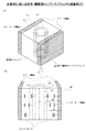
すなわち、キャパシタンスCは、誘電体ブロック1の比誘電率εrと真空中の誘電率εoと電極間距離dと電極間面積Sとで決まることが示されている。従って電極間距離dを短くすればするほどキャパシタンスCは増大することが分かる。また、キャパシタンスCは、誘電体ブロック1の材料として高い比誘電率のものを用いても同様に大きくすることが可能である。
スルーホール電極を内包する誘電体を挟んで該スルーホール電極から離れた位置に設けたアース電極を有する第1のコンデンサブロックと、
スルーホール電極を内包する誘電体を挟んで該スルーホール電極から離れた位置に設けたアース電極を備え、該両電極間を電気的に接続した第2のコンデンサブロックとを有し、
該第1のコンデンサブロックのアース電極と該第2のコンデンサブロックのアース電極とが電気的に接続されたことを特徴とするコンデンサシート。
(付記2)付記1において、
各コンデンサブロックが立方体又は直方体であり、該スルーホール電極が該立方体又は直方体の2面のほぼ中央部を貫通するように設けられ、該スルーホール電極とは交差しない該立方体又は直方体の対向する2面に該アース電極が設けられていることを特徴としたコンデンサシート。
(付記3)付記2において、
隣接するコンデンサブロック同士を、互いに同じ方向で結合しても、それぞれのコンデンサブロックのアース電極が電気的に接続されるように該アース電極がコンデンサブロックに設けられていることを特徴としたコンデンサシート。
(付記4)付記2おいて、
各コンデンサブロックが立方体の場合、隣接するコンデンサブロック同士を、互いに90°回転させて結合してもそれぞれのコンデンサブロックのアース電極が電気的に接続されるように該アース電極がコンデンサブロックに設けられていることを特徴としたコンデンサシート。
(付記5)付記1おいて、
該第1コンデンサブロックのスルーホール電極は、該アース電極と共に形成されるキャパシタンスが所望の値になるような直径及び長さを有する円筒形を有していることを特徴としたコンデンサシート。
(付記6)付記5おいて、
該直径が異なるスルーホール電極を有する複数個のコンデンサブロックを、所望のキャパシタンスに合わせて配置したことを特徴としたコンデンサシート。
(付記7)付記5おいて、
該第1のコンデンサブロックが、所望のキャパシタンスに合わせたサイズの立方体又は直方体であることを特徴としたコンデンサシート。
(付記8)付記1おいて、
該第1のコンデンサブロックが、所望の特性インピーダンスを与える直径のスルーホール電極を有していることを特徴としたコンデンサシート。
(付記9)付記1おいて、
全てのアース電極同士、又は一部のアース電極同士が電気的に接続されるように各コンデンサブロックが配置されていることを特徴としたコンデンサシート。
(付記10)付記1おいて、
該回路基板の内の一枚がBGAで、もう一枚がプリント配線板であり、該スルーホール電極の一端を、その上に設けたフットプリントを介して該BGAに接続すると共に、該スルーホール電極の他端を、その上に設けたバンプを介して該プリント配線板に接続することを特徴としたコンデンサシート。
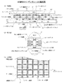
2, 2_1〜2_3 スルーホール電極
3 アース電極
4 パターン配線
10 信号・電源用コンデンサブロック
11 アース用コンデンサブロック
12 コンデンサシート
21 BGA(ボール・グリッド・アレイ)
141, 212 アース用バンプ(電極)
142, 212 信号・電源用バンプ
131, 221 アース用フットプリント
132, 222 信号・電源用フットプリント
31 I/O電源用電極
32 コア用電極
41 I/O電源用スルーホール電極
42 コア用スルーホール電極
101 電源電極用コンデンサブロック
102 信号電極用コンデンサブロック
110 アース電極用コンデンサブロック
図中、同一符号は同一又は相当部分を示す。
Claims (5)
- スルーホール電極を内包する誘電体を挟んで該スルーホール電極から離れた位置に設けたアース電極を有する第1のコンデンサブロックと、
スルーホール電極を内包する誘電体を挟んで該スルーホール電極から離れた位置に設けたアース電極を備え、該両電極間を電気的に接続した第2のコンデンサブロックとを有し、
該第1のコンデンサブロックのアース電極と該第2のコンデンサブロックのアース電極とが電気的に接続されたことを特徴とするコンデンサシート。 - 請求項1において、
各コンデンサブロックが立方体又は直方体であり、該スルーホール電極が該立方体又は直方体の2面のほぼ中央部を貫通するように設けられ、該スルーホール電極とは交差しない該立方体又は直方体の対向する2面に該アース電極が設けられていることを特徴としたコンデンサシート。 - 請求項2において、
隣接するコンデンサブロック同士を、互いに同じ方向で結合しても、それぞれのコンデンサブロックのアース電極が電気的に接続されるように該アース電極がコンデンサブロックに設けられていることを特徴としたコンデンサシート。 - 請求項2おいて、
各コンデンサブロックが立方体の場合、隣接するコンデンサブロック同士を、互いに90°回転させて結合してもそれぞれのコンデンサブロックのアース電極が電気的に接続されるように該アース電極がコンデンサブロックに設けられていることを特徴としたコンデンサシート。 - 請求項1おいて、
該第1コンデンサブロックのスルーホール電極は、該アース電極と共に形成されるキャパシタンスが所望の値になるような直径及び長さを有する円筒形を有していることを特徴としたコンデンサシート。
Priority Applications (2)
| Application Number | Priority Date | Filing Date | Title |
|---|---|---|---|
| JP2004042877A JP4338545B2 (ja) | 2004-02-19 | 2004-02-19 | コンデンサシート |
| US10/878,919 US6859352B1 (en) | 2004-02-19 | 2004-06-28 | Capacitor sheet |
Applications Claiming Priority (1)
| Application Number | Priority Date | Filing Date | Title |
|---|---|---|---|
| JP2004042877A JP4338545B2 (ja) | 2004-02-19 | 2004-02-19 | コンデンサシート |
Publications (2)
| Publication Number | Publication Date |
|---|---|
| JP2005236008A JP2005236008A (ja) | 2005-09-02 |
| JP4338545B2 true JP4338545B2 (ja) | 2009-10-07 |
Family
ID=34132081
Family Applications (1)
| Application Number | Title | Priority Date | Filing Date |
|---|---|---|---|
| JP2004042877A Expired - Fee Related JP4338545B2 (ja) | 2004-02-19 | 2004-02-19 | コンデンサシート |
Country Status (2)
| Country | Link |
|---|---|
| US (1) | US6859352B1 (ja) |
| JP (1) | JP4338545B2 (ja) |
Families Citing this family (10)
| Publication number | Priority date | Publication date | Assignee | Title |
|---|---|---|---|---|
| US7829875B2 (en) * | 2006-03-31 | 2010-11-09 | Sandisk 3D Llc | Nonvolatile rewritable memory cell comprising a resistivity-switching oxide or nitride and an antifuse |
| JP4283834B2 (ja) * | 2006-09-06 | 2009-06-24 | Tdk株式会社 | 積層コンデンサ |
| JP5133813B2 (ja) * | 2008-08-11 | 2013-01-30 | レノボ・シンガポール・プライベート・リミテッド | 積層セラミック・コンデンサの単位配置構造、全体配置構造およびプリント配線基板 |
| JP2010258301A (ja) * | 2009-04-27 | 2010-11-11 | Shinko Electric Ind Co Ltd | インターポーザ及び半導体装置 |
| US8633398B2 (en) | 2011-10-25 | 2014-01-21 | Hewlett-Packard Development Company, L.P. | Circuit board contact pads |
| JP6323672B2 (ja) * | 2014-07-25 | 2018-05-16 | 株式会社ソシオネクスト | 半導体装置及びその製造方法 |
| US10141277B2 (en) * | 2017-03-31 | 2018-11-27 | International Business Machines Corporation | Monolithic decoupling capacitor between solder bumps |
| JP7619315B2 (ja) * | 2022-03-26 | 2025-01-22 | 株式会社村田製作所 | 積層セラミックコンデンサ |
| CN117560860A (zh) * | 2022-08-04 | 2024-02-13 | 辉达公司 | 堆叠多个印刷电路板的方法和配置 |
| CN115565785B (zh) * | 2022-10-18 | 2025-09-16 | 安徽锐光电子科技有限公司 | 一种可调节式云母片电容器 |
Family Cites Families (11)
| Publication number | Priority date | Publication date | Assignee | Title |
|---|---|---|---|---|
| US5428499A (en) * | 1993-01-28 | 1995-06-27 | Storage Technology Corporation | Printed circuit board having integrated decoupling capacitive core with discrete elements |
| JPH07321585A (ja) | 1994-05-30 | 1995-12-08 | Witco Of Jupiter Dentsu Kk | ノイズフィルタ |
| JPH08181445A (ja) | 1994-12-22 | 1996-07-12 | Sumitomo Metal Ind Ltd | セラミックス多層基板 |
| JP3475581B2 (ja) | 1995-06-27 | 2003-12-08 | 松下電工株式会社 | 電動歯ブラシ |
| JPH09102432A (ja) | 1995-10-05 | 1997-04-15 | Canon Inc | バイパスコンデンサ及びその形成方法 |
| JP3696341B2 (ja) * | 1996-08-30 | 2005-09-14 | ローム株式会社 | アレイ型固体電解コンデンサの構造及びその製造方法 |
| JPH10322022A (ja) | 1997-05-19 | 1998-12-04 | Nec Corp | 多層プリント基板 |
| JPH11307389A (ja) * | 1998-04-24 | 1999-11-05 | Mitsubishi Electric Corp | パターンコンデンサ |
| US6625006B1 (en) * | 2000-09-05 | 2003-09-23 | Marvell International, Ltd. | Fringing capacitor structure |
| JP2003124430A (ja) | 2001-10-16 | 2003-04-25 | Nec Corp | 集積回路装置および集積回路用コンデンサ |
| US6614645B1 (en) * | 2002-11-12 | 2003-09-02 | National Semiconductor Corporation | Matched capacitor array |
-
2004
- 2004-02-19 JP JP2004042877A patent/JP4338545B2/ja not_active Expired - Fee Related
- 2004-06-28 US US10/878,919 patent/US6859352B1/en not_active Expired - Lifetime
Also Published As
| Publication number | Publication date |
|---|---|
| JP2005236008A (ja) | 2005-09-02 |
| US6859352B1 (en) | 2005-02-22 |
Similar Documents
| Publication | Publication Date | Title |
|---|---|---|
| KR100364967B1 (ko) | 적층 커패시터, 배선 기판, 및 고주파 회로 | |
| KR100363652B1 (ko) | 다층 커패시터, 배선기판, 감결합 회로 및 고주파 회로 | |
| KR100240525B1 (ko) | 반도체장치 및 그것을 사용한 전자장치 | |
| KR100364009B1 (ko) | 다층 커패시터, 배선기판, 감결합 회로 및 고주파 회로 | |
| US6327134B1 (en) | Multi-layer capacitor, wiring board, and high-frequency circuit | |
| US6384476B2 (en) | Semiconductor integrated circuit and printed wiring substrate provided with the same | |
| US7271348B1 (en) | Providing decoupling capacitors in a circuit board | |
| US20040027813A1 (en) | Manufacturing methods for an electronic assembly with vertically connected capacitors | |
| US6999299B2 (en) | Capacitor structure, a multi-layer wiring board including the same, and a semiconductor device using the multi-layer wiring board | |
| JP4338545B2 (ja) | コンデンサシート | |
| US7791896B1 (en) | Providing an embedded capacitor in a circuit board | |
| US6683781B2 (en) | Packaging structure with low switching noises | |
| JP2007250928A (ja) | 多層プリント配線板 | |
| CN105789183A (zh) | 半导体器件 | |
| WO2022071235A1 (ja) | 回路モジュール | |
| JP2007305642A (ja) | 多層回路基板及び電子装置 | |
| JP4280179B2 (ja) | 積層型半導体装置 | |
| JP4243621B2 (ja) | 半導体パッケージ | |
| KR102796616B1 (ko) | 전원공급 보조장치를 구비한 인쇄회로기판, 및 이를 구비한 전자기기 | |
| JP2005277115A (ja) | チップコンデンサ実装構造及びプリント配線板 | |
| JP7405460B1 (ja) | 回路基板および電子部品の製造方法 | |
| JP2007129046A (ja) | コンデンサアレイの実装構造 | |
| US20090001548A1 (en) | Semiconductor package | |
| JP2005203420A (ja) | 電子回路基板 | |
| JP6136061B2 (ja) | 半導体装置 |
Legal Events
| Date | Code | Title | Description |
|---|---|---|---|
| A621 | Written request for application examination |
Free format text: JAPANESE INTERMEDIATE CODE: A621 Effective date: 20070208 |
|
| TRDD | Decision of grant or rejection written | ||
| A01 | Written decision to grant a patent or to grant a registration (utility model) |
Free format text: JAPANESE INTERMEDIATE CODE: A01 Effective date: 20090630 |
|
| A01 | Written decision to grant a patent or to grant a registration (utility model) |
Free format text: JAPANESE INTERMEDIATE CODE: A01 |
|
| A61 | First payment of annual fees (during grant procedure) |
Free format text: JAPANESE INTERMEDIATE CODE: A61 Effective date: 20090630 |
|
| R150 | Certificate of patent or registration of utility model |
Ref document number: 4338545 Country of ref document: JP Free format text: JAPANESE INTERMEDIATE CODE: R150 Free format text: JAPANESE INTERMEDIATE CODE: R150 |
|
| FPAY | Renewal fee payment (event date is renewal date of database) |
Free format text: PAYMENT UNTIL: 20120710 Year of fee payment: 3 |
|
| FPAY | Renewal fee payment (event date is renewal date of database) |
Free format text: PAYMENT UNTIL: 20120710 Year of fee payment: 3 |
|
| FPAY | Renewal fee payment (event date is renewal date of database) |
Free format text: PAYMENT UNTIL: 20130710 Year of fee payment: 4 |
|
| LAPS | Cancellation because of no payment of annual fees |