JP4353145B2 - 液滴吐出装置 - Google Patents
液滴吐出装置 Download PDFInfo
- Publication number
- JP4353145B2 JP4353145B2 JP2005189508A JP2005189508A JP4353145B2 JP 4353145 B2 JP4353145 B2 JP 4353145B2 JP 2005189508 A JP2005189508 A JP 2005189508A JP 2005189508 A JP2005189508 A JP 2005189508A JP 4353145 B2 JP4353145 B2 JP 4353145B2
- Authority
- JP
- Japan
- Prior art keywords
- droplet
- droplet discharge
- droplets
- laser
- stage
- Prior art date
- Legal status (The legal status is an assumption and is not a legal conclusion. Google has not performed a legal analysis and makes no representation as to the accuracy of the status listed.)
- Expired - Fee Related
Links
Images





Classifications
-
- H—ELECTRICITY
- H05—ELECTRIC TECHNIQUES NOT OTHERWISE PROVIDED FOR
- H05K—PRINTED CIRCUITS; CASINGS OR CONSTRUCTIONAL DETAILS OF ELECTRIC APPARATUS; MANUFACTURE OF ASSEMBLAGES OF ELECTRICAL COMPONENTS
- H05K3/00—Apparatus or processes for manufacturing printed circuits
- H05K3/10—Apparatus or processes for manufacturing printed circuits in which conductive material is applied to the insulating support in such a manner as to form the desired conductive pattern
- H05K3/12—Apparatus or processes for manufacturing printed circuits in which conductive material is applied to the insulating support in such a manner as to form the desired conductive pattern using thick film techniques, e.g. printing techniques to apply the conductive material or similar techniques for applying conductive paste or ink patterns
- H05K3/1241—Apparatus or processes for manufacturing printed circuits in which conductive material is applied to the insulating support in such a manner as to form the desired conductive pattern using thick film techniques, e.g. printing techniques to apply the conductive material or similar techniques for applying conductive paste or ink patterns by ink-jet printing or drawing by dispensing
- H05K3/125—Apparatus or processes for manufacturing printed circuits in which conductive material is applied to the insulating support in such a manner as to form the desired conductive pattern using thick film techniques, e.g. printing techniques to apply the conductive material or similar techniques for applying conductive paste or ink patterns by ink-jet printing or drawing by dispensing by ink-jet printing
-
- H—ELECTRICITY
- H10—SEMICONDUCTOR DEVICES; ELECTRIC SOLID-STATE DEVICES NOT OTHERWISE PROVIDED FOR
- H10W—GENERIC PACKAGES, INTERCONNECTIONS, CONNECTORS OR OTHER CONSTRUCTIONAL DETAILS OF DEVICES COVERED BY CLASS H10
- H10W20/00—Interconnections in chips, wafers or substrates
- H10W20/01—Manufacture or treatment
- H10W20/031—Manufacture or treatment of conductive parts of the interconnections
-
- B—PERFORMING OPERATIONS; TRANSPORTING
- B41—PRINTING; LINING MACHINES; TYPEWRITERS; STAMPS
- B41J—TYPEWRITERS; SELECTIVE PRINTING MECHANISMS, i.e. MECHANISMS PRINTING OTHERWISE THAN FROM A FORME; CORRECTION OF TYPOGRAPHICAL ERRORS
- B41J11/00—Devices or arrangements of selective printing mechanisms, e.g. ink-jet printers or thermal printers, for supporting or handling copy material in sheet or web form
- B41J11/0015—Devices or arrangements of selective printing mechanisms, e.g. ink-jet printers or thermal printers, for supporting or handling copy material in sheet or web form for treating before, during or after printing or for uniform coating or laminating the copy material before or after printing
- B41J11/002—Curing or drying the ink on the copy materials, e.g. by heating or irradiating
- B41J11/0021—Curing or drying the ink on the copy materials, e.g. by heating or irradiating using irradiation
-
- G—PHYSICS
- G03—PHOTOGRAPHY; CINEMATOGRAPHY; ANALOGOUS TECHNIQUES USING WAVES OTHER THAN OPTICAL WAVES; ELECTROGRAPHY; HOLOGRAPHY
- G03F—PHOTOMECHANICAL PRODUCTION OF TEXTURED OR PATTERNED SURFACES, e.g. FOR PRINTING, FOR PROCESSING OF SEMICONDUCTOR DEVICES; MATERIALS THEREFOR; ORIGINALS THEREFOR; APPARATUS SPECIALLY ADAPTED THEREFOR
- G03F7/00—Photomechanical, e.g. photolithographic, production of textured or patterned surfaces, e.g. printing surfaces; Materials therefor, e.g. comprising photoresists; Apparatus specially adapted therefor
- G03F7/0002—Lithographic processes using patterning methods other than those involving the exposure to radiation, e.g. by stamping
-
- G—PHYSICS
- G03—PHOTOGRAPHY; CINEMATOGRAPHY; ANALOGOUS TECHNIQUES USING WAVES OTHER THAN OPTICAL WAVES; ELECTROGRAPHY; HOLOGRAPHY
- G03F—PHOTOMECHANICAL PRODUCTION OF TEXTURED OR PATTERNED SURFACES, e.g. FOR PRINTING, FOR PROCESSING OF SEMICONDUCTOR DEVICES; MATERIALS THEREFOR; ORIGINALS THEREFOR; APPARATUS SPECIALLY ADAPTED THEREFOR
- G03F7/00—Photomechanical, e.g. photolithographic, production of textured or patterned surfaces, e.g. printing surfaces; Materials therefor, e.g. comprising photoresists; Apparatus specially adapted therefor
- G03F7/20—Exposure; Apparatus therefor
- G03F7/2002—Exposure; Apparatus therefor with visible light or UV light, through an original having an opaque pattern on a transparent support, e.g. film printing, projection printing; by reflection of visible or UV light from an original such as a printed image
- G03F7/2014—Contact or film exposure of light sensitive plates such as lithographic plates or circuit boards, e.g. in a vacuum frame
- G03F7/2016—Contact mask being integral part of the photosensitive element and subject to destructive removal during post-exposure processing
- G03F7/2018—Masking pattern obtained by selective application of an ink or a toner, e.g. ink jet printing
-
- H—ELECTRICITY
- H05—ELECTRIC TECHNIQUES NOT OTHERWISE PROVIDED FOR
- H05K—PRINTED CIRCUITS; CASINGS OR CONSTRUCTIONAL DETAILS OF ELECTRIC APPARATUS; MANUFACTURE OF ASSEMBLAGES OF ELECTRICAL COMPONENTS
- H05K3/00—Apparatus or processes for manufacturing printed circuits
- H05K3/10—Apparatus or processes for manufacturing printed circuits in which conductive material is applied to the insulating support in such a manner as to form the desired conductive pattern
- H05K3/12—Apparatus or processes for manufacturing printed circuits in which conductive material is applied to the insulating support in such a manner as to form the desired conductive pattern using thick film techniques, e.g. printing techniques to apply the conductive material or similar techniques for applying conductive paste or ink patterns
- H05K3/1283—After-treatment of the printed patterns, e.g. sintering or curing methods
-
- H—ELECTRICITY
- H05—ELECTRIC TECHNIQUES NOT OTHERWISE PROVIDED FOR
- H05K—PRINTED CIRCUITS; CASINGS OR CONSTRUCTIONAL DETAILS OF ELECTRIC APPARATUS; MANUFACTURE OF ASSEMBLAGES OF ELECTRICAL COMPONENTS
- H05K3/00—Apparatus or processes for manufacturing printed circuits
- H05K3/10—Apparatus or processes for manufacturing printed circuits in which conductive material is applied to the insulating support in such a manner as to form the desired conductive pattern
- H05K3/12—Apparatus or processes for manufacturing printed circuits in which conductive material is applied to the insulating support in such a manner as to form the desired conductive pattern using thick film techniques, e.g. printing techniques to apply the conductive material or similar techniques for applying conductive paste or ink patterns
- H05K3/1283—After-treatment of the printed patterns, e.g. sintering or curing methods
- H05K3/1291—Firing or sintering at relative high temperatures for patterns on inorganic boards, e.g. co-firing of circuits on green ceramic sheets
-
- H—ELECTRICITY
- H10—SEMICONDUCTOR DEVICES; ELECTRIC SOLID-STATE DEVICES NOT OTHERWISE PROVIDED FOR
- H10K—ORGANIC ELECTRIC SOLID-STATE DEVICES
- H10K71/00—Manufacture or treatment specially adapted for the organic devices covered by this subclass
- H10K71/60—Forming conductive regions or layers, e.g. electrodes
- H10K71/611—Forming conductive regions or layers, e.g. electrodes using printing deposition, e.g. ink jet printing
-
- H—ELECTRICITY
- H10—SEMICONDUCTOR DEVICES; ELECTRIC SOLID-STATE DEVICES NOT OTHERWISE PROVIDED FOR
- H10P—GENERIC PROCESSES OR APPARATUS FOR THE MANUFACTURE OR TREATMENT OF DEVICES COVERED BY CLASS H10
- H10P14/00—Formation of materials, e.g. in the shape of layers or pillars
- H10P14/40—Formation of materials, e.g. in the shape of layers or pillars of conductive or resistive materials
- H10P14/46—Formation of materials, e.g. in the shape of layers or pillars of conductive or resistive materials using a liquid
-
- H—ELECTRICITY
- H05—ELECTRIC TECHNIQUES NOT OTHERWISE PROVIDED FOR
- H05K—PRINTED CIRCUITS; CASINGS OR CONSTRUCTIONAL DETAILS OF ELECTRIC APPARATUS; MANUFACTURE OF ASSEMBLAGES OF ELECTRICAL COMPONENTS
- H05K2203/00—Indexing scheme relating to apparatus or processes for manufacturing printed circuits covered by H05K3/00
- H05K2203/10—Using electric, magnetic and electromagnetic fields; Using laser light
- H05K2203/107—Using laser light
Landscapes
- Engineering & Computer Science (AREA)
- Manufacturing & Machinery (AREA)
- Microelectronics & Electronic Packaging (AREA)
- General Physics & Mathematics (AREA)
- Physics & Mathematics (AREA)
- Inorganic Chemistry (AREA)
- Chemical & Material Sciences (AREA)
- Ceramic Engineering (AREA)
- Health & Medical Sciences (AREA)
- General Health & Medical Sciences (AREA)
- Toxicology (AREA)
- Coating Apparatus (AREA)
- Manufacturing Of Printed Wiring (AREA)
- Application Of Or Painting With Fluid Materials (AREA)
Description
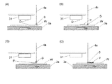
2 基台(防振台)
2a ブリッジ
3 描画系
4 光学系
4a,4b,4c 第1〜第3の光路
5 撮像系
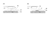
31 液滴吐出ヘッド
32 キャリッジ
33 キャリッジ用θ方向回転体
33 ゴニオステージ
34 キャリッジ用Z軸方向移動体
35 キャリッジ用フィード方向移動体
3a ステージ
3b ステージ用θ方向回転体
3c ステージ用フィード方向移動体
3d ステージ用スキャン方向移動体
40 レーザ光源
51 第1のCCDカメラ(第1の電子カメラ)
52 第1のCCDカメラ用Z軸方向移動体
53 第2のCCDカメラ(第2の電子カメラ)
55 仕切り
56 ビームディフューザ
60 制御部
D 液滴
P 配線パターン
S レーザスポット
Claims (5)
- 基台と、
機能液を液滴にして吐出する液滴吐出ヘッドと、前記液滴吐出ヘッドを保持するキャリッジと、前記液滴が描画されるワークを保持するステージと、
レーザ光を出力する光源と、
_前記液滴吐出ヘッドを覆う保護カバーと、
を有し、
_前記レーザ光は、前記ステージに対して平行な方向から前記液滴に照射され、
_前記保護カバーに前記レーザ光を照射することによって、前記レーザ光の光路を調整することを特徴とする液滴吐出装置。 - 前記基台上に設けられ、前記ワークと前記液滴の着弾位置のアライメントをとるための第1のカメラと、前記液滴の着弾位置と前記レーザ光のレーザスポットのアライメントをとるための第2のカメラと、を有することを特徴とする請求項1記載の液滴吐出装置。
- 前記キャリッジ及び前記液滴吐出ヘッドは前記基台に対して位置が固定され、前記ステージが移動して描画を行うことを特徴とする請求項1記載の液滴吐出装置。
- 前記機能液は電気的素子、光学的素子又は電気光学的素子の材料を含み、
前記液滴を前記ワーク上に吐出して所定のパターンを描画し、前記液滴に前記レーザ光を照射することによりパターンを定着させることを特徴とする請求項1記載の液滴吐出装置。 - 前記機能液は導電性粒子を含み、
前記液滴を前記ワーク上に吐出して所定のパターンを描画し、前記液滴に前記レーザ光を照射することにより該液滴を乾燥し前記導電性粒子を焼結させて配線パターンを形成することを特徴とする請求項1記載の液滴吐出装置。
Priority Applications (5)
| Application Number | Priority Date | Filing Date | Title |
|---|---|---|---|
| JP2005189508A JP4353145B2 (ja) | 2005-06-29 | 2005-06-29 | 液滴吐出装置 |
| US11/421,545 US7726803B2 (en) | 2005-06-29 | 2006-06-01 | Droplet ejection apparatus |
| TW095122948A TWI301800B (en) | 2005-06-29 | 2006-06-26 | Droplet ejection apparatus |
| KR1020060058018A KR100786211B1 (ko) | 2005-06-29 | 2006-06-27 | 액적 토출 장치 |
| CN2006100956985A CN1891461B (zh) | 2005-06-29 | 2006-06-29 | 液滴喷出装置 |
Applications Claiming Priority (1)
| Application Number | Priority Date | Filing Date | Title |
|---|---|---|---|
| JP2005189508A JP4353145B2 (ja) | 2005-06-29 | 2005-06-29 | 液滴吐出装置 |
Publications (2)
| Publication Number | Publication Date |
|---|---|
| JP2007007522A JP2007007522A (ja) | 2007-01-18 |
| JP4353145B2 true JP4353145B2 (ja) | 2009-10-28 |
Family
ID=37588941
Family Applications (1)
| Application Number | Title | Priority Date | Filing Date |
|---|---|---|---|
| JP2005189508A Expired - Fee Related JP4353145B2 (ja) | 2005-06-29 | 2005-06-29 | 液滴吐出装置 |
Country Status (5)
| Country | Link |
|---|---|
| US (1) | US7726803B2 (ja) |
| JP (1) | JP4353145B2 (ja) |
| KR (1) | KR100786211B1 (ja) |
| CN (1) | CN1891461B (ja) |
| TW (1) | TWI301800B (ja) |
Cited By (2)
| Publication number | Priority date | Publication date | Assignee | Title |
|---|---|---|---|---|
| JP2013063371A (ja) * | 2011-09-15 | 2013-04-11 | Ricoh Co Ltd | 薄膜製造装置のアライメント調整方法、薄膜製造装置、該薄膜製造装置により製造した電気機械変換膜、電気機械変換素子、液滴吐出ヘッド及び液滴吐出装置 |
| US8833921B2 (en) | 2010-07-30 | 2014-09-16 | Ricoh Company, Limited | Thin-film forming apparatus, thin-film forming method, piezoelectric-element forming method, droplet discharging head, and ink-jet recording apparatus |
Families Citing this family (7)
| Publication number | Priority date | Publication date | Assignee | Title |
|---|---|---|---|---|
| JP4442677B2 (ja) * | 2007-10-11 | 2010-03-31 | セイコーエプソン株式会社 | 液滴吐出装置の液滴乾燥方法及び液滴吐出装置 |
| CN102407665B (zh) * | 2010-07-30 | 2015-03-04 | 株式会社理光 | 薄膜形成设备及方法、压电元件形成方法、排放头和设备 |
| CN112549529B (zh) * | 2014-07-13 | 2022-11-29 | 斯特拉塔西斯公司 | 用于三维打印的系统及制造三维物体的方法 |
| JP6390407B2 (ja) * | 2014-12-16 | 2018-09-19 | 富士ゼロックス株式会社 | 乾燥装置、画像形成装置、及び乾燥プログラム |
| NL2016137B1 (en) * | 2016-01-21 | 2017-07-25 | Meyer Burger (Netherlands) B V | Inkjet printing system and method for processing substrates. |
| CN111822256A (zh) * | 2020-07-30 | 2020-10-27 | 重庆盛泰光电有限公司 | 基于转盘的摄像头模组点胶系统 |
| KR102882014B1 (ko) * | 2023-04-14 | 2025-11-12 | (주)트리엔 | 레이저 직접 조사 방식의 레이저 열처리 방법, 상기 방법을 지원하는 시스템, 및 상기 방법에 따라 제조된 전장부품 |
Family Cites Families (16)
| Publication number | Priority date | Publication date | Assignee | Title |
|---|---|---|---|---|
| US5132248A (en) | 1988-05-31 | 1992-07-21 | The United States Of America As Represented By The United States Department Of Energy | Direct write with microelectronic circuit fabrication |
| GB2233928B (en) * | 1989-05-23 | 1992-12-23 | Brother Ind Ltd | Apparatus and method for forming three-dimensional article |
| EP1223615A1 (en) | 2001-01-10 | 2002-07-17 | Eidgenössische Technische Hochschule Zürich | A method for producing a structure using nanoparticles |
| GB2379413A (en) | 2001-09-10 | 2003-03-12 | Seiko Epson Corp | Printhead alignment method |
| JP2003318193A (ja) | 2002-04-22 | 2003-11-07 | Seiko Epson Corp | デバイス、その製造方法及び電子装置 |
| JP2003326691A (ja) | 2002-05-09 | 2003-11-19 | Konica Minolta Holdings Inc | 画像記録方法、エネルギー線硬化インク及び画像記録装置 |
| JP4741192B2 (ja) * | 2003-01-17 | 2011-08-03 | 株式会社半導体エネルギー研究所 | 半導体装置の作製方法 |
| JP4225076B2 (ja) * | 2003-02-19 | 2009-02-18 | セイコーエプソン株式会社 | 液滴吐出装置 |
| JP4244382B2 (ja) * | 2003-02-26 | 2009-03-25 | セイコーエプソン株式会社 | 機能性材料定着方法及びデバイス製造方法 |
| JP2004337709A (ja) * | 2003-05-14 | 2004-12-02 | Seiko Epson Corp | 液滴吐出装置、カラーフィルター製造装置、カラーフィルター及びその製造方法、液晶装置、電子機器 |
| JP4232541B2 (ja) * | 2003-06-04 | 2009-03-04 | セイコーエプソン株式会社 | マイクロレンズ装置の製造方法 |
| JP2005040665A (ja) | 2003-07-23 | 2005-02-17 | Fuji Photo Film Co Ltd | パターン形成方法およびパターン形成装置 |
| JP2005081159A (ja) * | 2003-09-04 | 2005-03-31 | Ricoh Co Ltd | 機能性基体製造装置ならびに製造される機能性基体 |
| JP3941066B2 (ja) | 2003-09-11 | 2007-07-04 | 俊次 村野 | ライン状均一吐出装置、霧化装置、薄膜形成装置、パターン形成装置、三次元造形装置および洗浄装置。 |
| JP2006035184A (ja) | 2004-07-30 | 2006-02-09 | Seiko Epson Corp | 液滴塗布方法と液滴塗布装置及び電気光学装置並びに電子機器 |
| JP4715147B2 (ja) | 2004-09-28 | 2011-07-06 | セイコーエプソン株式会社 | 導電膜の形成方法 |
-
2005
- 2005-06-29 JP JP2005189508A patent/JP4353145B2/ja not_active Expired - Fee Related
-
2006
- 2006-06-01 US US11/421,545 patent/US7726803B2/en not_active Expired - Fee Related
- 2006-06-26 TW TW095122948A patent/TWI301800B/zh not_active IP Right Cessation
- 2006-06-27 KR KR1020060058018A patent/KR100786211B1/ko not_active Expired - Fee Related
- 2006-06-29 CN CN2006100956985A patent/CN1891461B/zh not_active Expired - Fee Related
Cited By (2)
| Publication number | Priority date | Publication date | Assignee | Title |
|---|---|---|---|---|
| US8833921B2 (en) | 2010-07-30 | 2014-09-16 | Ricoh Company, Limited | Thin-film forming apparatus, thin-film forming method, piezoelectric-element forming method, droplet discharging head, and ink-jet recording apparatus |
| JP2013063371A (ja) * | 2011-09-15 | 2013-04-11 | Ricoh Co Ltd | 薄膜製造装置のアライメント調整方法、薄膜製造装置、該薄膜製造装置により製造した電気機械変換膜、電気機械変換素子、液滴吐出ヘッド及び液滴吐出装置 |
Also Published As
| Publication number | Publication date |
|---|---|
| JP2007007522A (ja) | 2007-01-18 |
| US20070002114A1 (en) | 2007-01-04 |
| US7726803B2 (en) | 2010-06-01 |
| CN1891461B (zh) | 2010-12-08 |
| KR20070001805A (ko) | 2007-01-04 |
| KR100786211B1 (ko) | 2007-12-17 |
| TWI301800B (en) | 2008-10-11 |
| CN1891461A (zh) | 2007-01-10 |
| TW200706381A (en) | 2007-02-16 |
Similar Documents
| Publication | Publication Date | Title |
|---|---|---|
| EP3294528B1 (en) | Additive manufacturing apparatus and method | |
| KR101385797B1 (ko) | 증착 복구 장치 및 방법 | |
| KR101395157B1 (ko) | 박막 형성 장치 및 박막 형성 방법 | |
| JP4353145B2 (ja) | 液滴吐出装置 | |
| JP2010539704A (ja) | 電子材料のレーザデカール転写 | |
| WO2018181344A1 (ja) | 処理方法及び処理システム | |
| WO2016185215A1 (en) | A circuit board and component fabrication apparatus | |
| KR101979539B1 (ko) | 프린팅 장치 | |
| CN109746572B (zh) | 激光加工装置 | |
| KR20220102107A (ko) | 레이저 가공 장치 | |
| TW201420208A (zh) | 基板製造方法及基板製造裝置 | |
| KR102030888B1 (ko) | 액체 토출 장치, 임프린트 장치 및 물품 제조 방법 | |
| US20170057154A1 (en) | Imprint apparatus, imprint method, and method of producing article | |
| JP7440954B2 (ja) | 薄膜形成装置および薄膜形成方法 | |
| JP7118712B2 (ja) | インプリント装置、インプリント方法、および物品の製造方法 | |
| JP6871435B2 (ja) | インクジェット印刷装置 | |
| KR102239964B1 (ko) | 임프린트 장치, 및 물품의 제조 방법 | |
| JP6721747B2 (ja) | インクジェット方式の薄膜形成装置 | |
| JP2005069900A (ja) | 集光点位置検出方法、集光点位置検出装置、液滴観測方法、液滴観測装置および液滴吐出装置 | |
| JP7059046B2 (ja) | 型を用いて基板上の組成物を成形する成形装置、および物品の製造方法 | |
| JP2019036572A (ja) | インプリント装置、インプリント方法および、物品製造方法 | |
| JP2020042182A (ja) | フレネルレンズ及びフレネルレンズの製造方法 | |
| JP2022077266A (ja) | 基板処理装置、基板処理方法、及び物品の製造方法 | |
| JP2019009230A (ja) | インプリント装置、インプリント方法、および物品の製造方法 | |
| JP2018099634A (ja) | インクジェット塗布装置、及び、膜パターン形成方法 |
Legal Events
| Date | Code | Title | Description |
|---|---|---|---|
| RD04 | Notification of resignation of power of attorney |
Free format text: JAPANESE INTERMEDIATE CODE: A7424 Effective date: 20070404 |
|
| A977 | Report on retrieval |
Free format text: JAPANESE INTERMEDIATE CODE: A971007 Effective date: 20090220 |
|
| A131 | Notification of reasons for refusal |
Free format text: JAPANESE INTERMEDIATE CODE: A131 Effective date: 20090331 |
|
| A521 | Request for written amendment filed |
Free format text: JAPANESE INTERMEDIATE CODE: A523 Effective date: 20090525 |
|
| TRDD | Decision of grant or rejection written | ||
| A01 | Written decision to grant a patent or to grant a registration (utility model) |
Free format text: JAPANESE INTERMEDIATE CODE: A01 Effective date: 20090707 |
|
| A01 | Written decision to grant a patent or to grant a registration (utility model) |
Free format text: JAPANESE INTERMEDIATE CODE: A01 |
|
| A61 | First payment of annual fees (during grant procedure) |
Free format text: JAPANESE INTERMEDIATE CODE: A61 Effective date: 20090720 |
|
| R150 | Certificate of patent or registration of utility model |
Free format text: JAPANESE INTERMEDIATE CODE: R150 |
|
| FPAY | Renewal fee payment (event date is renewal date of database) |
Free format text: PAYMENT UNTIL: 20120807 Year of fee payment: 3 |
|
| LAPS | Cancellation because of no payment of annual fees |