JP4355656B2 - 金属有機アミンと金属有機酸化物を用いて金属酸化物を形成するシステムおよび方法 - Google Patents
金属有機アミンと金属有機酸化物を用いて金属酸化物を形成するシステムおよび方法 Download PDFInfo
- Publication number
- JP4355656B2 JP4355656B2 JP2004531530A JP2004531530A JP4355656B2 JP 4355656 B2 JP4355656 B2 JP 4355656B2 JP 2004531530 A JP2004531530 A JP 2004531530A JP 2004531530 A JP2004531530 A JP 2004531530A JP 4355656 B2 JP4355656 B2 JP 4355656B2
- Authority
- JP
- Japan
- Prior art keywords
- substrate
- formula
- layer
- deposition
- precursor
- Prior art date
- Legal status (The legal status is an assumption and is not a legal conclusion. Google has not performed a legal analysis and makes no representation as to the accuracy of the status listed.)
- Expired - Lifetime
Links
Images

Classifications
-
- C—CHEMISTRY; METALLURGY
- C23—COATING METALLIC MATERIAL; COATING MATERIAL WITH METALLIC MATERIAL; CHEMICAL SURFACE TREATMENT; DIFFUSION TREATMENT OF METALLIC MATERIAL; COATING BY VACUUM EVAPORATION, BY SPUTTERING, BY ION IMPLANTATION OR BY CHEMICAL VAPOUR DEPOSITION, IN GENERAL; INHIBITING CORROSION OF METALLIC MATERIAL OR INCRUSTATION IN GENERAL
- C23C—COATING METALLIC MATERIAL; COATING MATERIAL WITH METALLIC MATERIAL; SURFACE TREATMENT OF METALLIC MATERIAL BY DIFFUSION INTO THE SURFACE, BY CHEMICAL CONVERSION OR SUBSTITUTION; COATING BY VACUUM EVAPORATION, BY SPUTTERING, BY ION IMPLANTATION OR BY CHEMICAL VAPOUR DEPOSITION, IN GENERAL
- C23C16/00—Chemical coating by decomposition of gaseous compounds, without leaving reaction products of surface material in the coating, i.e. chemical vapour deposition [CVD] processes
- C23C16/22—Chemical coating by decomposition of gaseous compounds, without leaving reaction products of surface material in the coating, i.e. chemical vapour deposition [CVD] processes characterised by the deposition of inorganic material, other than metallic material
- C23C16/30—Deposition of compounds, mixtures or solid solutions, e.g. borides, carbides, nitrides
- C23C16/40—Oxides
- C23C16/405—Oxides of refractory metals or yttrium
-
- C—CHEMISTRY; METALLURGY
- C23—COATING METALLIC MATERIAL; COATING MATERIAL WITH METALLIC MATERIAL; CHEMICAL SURFACE TREATMENT; DIFFUSION TREATMENT OF METALLIC MATERIAL; COATING BY VACUUM EVAPORATION, BY SPUTTERING, BY ION IMPLANTATION OR BY CHEMICAL VAPOUR DEPOSITION, IN GENERAL; INHIBITING CORROSION OF METALLIC MATERIAL OR INCRUSTATION IN GENERAL
- C23C—COATING METALLIC MATERIAL; COATING MATERIAL WITH METALLIC MATERIAL; SURFACE TREATMENT OF METALLIC MATERIAL BY DIFFUSION INTO THE SURFACE, BY CHEMICAL CONVERSION OR SUBSTITUTION; COATING BY VACUUM EVAPORATION, BY SPUTTERING, BY ION IMPLANTATION OR BY CHEMICAL VAPOUR DEPOSITION, IN GENERAL
- C23C16/00—Chemical coating by decomposition of gaseous compounds, without leaving reaction products of surface material in the coating, i.e. chemical vapour deposition [CVD] processes
- C23C16/22—Chemical coating by decomposition of gaseous compounds, without leaving reaction products of surface material in the coating, i.e. chemical vapour deposition [CVD] processes characterised by the deposition of inorganic material, other than metallic material
- C23C16/30—Deposition of compounds, mixtures or solid solutions, e.g. borides, carbides, nitrides
- C23C16/40—Oxides
-
- H—ELECTRICITY
- H10—SEMICONDUCTOR DEVICES; ELECTRIC SOLID-STATE DEVICES NOT OTHERWISE PROVIDED FOR
- H10P—GENERIC PROCESSES OR APPARATUS FOR THE MANUFACTURE OR TREATMENT OF DEVICES COVERED BY CLASS H10
- H10P14/00—Formation of materials, e.g. in the shape of layers or pillars
- H10P14/60—Formation of materials, e.g. in the shape of layers or pillars of insulating materials
- H10P14/66—Formation of materials, e.g. in the shape of layers or pillars of insulating materials characterised by the type of materials
- H10P14/668—Formation of materials, e.g. in the shape of layers or pillars of insulating materials characterised by the type of materials the materials being characterised by the deposition precursor materials
-
- C—CHEMISTRY; METALLURGY
- C23—COATING METALLIC MATERIAL; COATING MATERIAL WITH METALLIC MATERIAL; CHEMICAL SURFACE TREATMENT; DIFFUSION TREATMENT OF METALLIC MATERIAL; COATING BY VACUUM EVAPORATION, BY SPUTTERING, BY ION IMPLANTATION OR BY CHEMICAL VAPOUR DEPOSITION, IN GENERAL; INHIBITING CORROSION OF METALLIC MATERIAL OR INCRUSTATION IN GENERAL
- C23C—COATING METALLIC MATERIAL; COATING MATERIAL WITH METALLIC MATERIAL; SURFACE TREATMENT OF METALLIC MATERIAL BY DIFFUSION INTO THE SURFACE, BY CHEMICAL CONVERSION OR SUBSTITUTION; COATING BY VACUUM EVAPORATION, BY SPUTTERING, BY ION IMPLANTATION OR BY CHEMICAL VAPOUR DEPOSITION, IN GENERAL
- C23C16/00—Chemical coating by decomposition of gaseous compounds, without leaving reaction products of surface material in the coating, i.e. chemical vapour deposition [CVD] processes
- C23C16/44—Chemical coating by decomposition of gaseous compounds, without leaving reaction products of surface material in the coating, i.e. chemical vapour deposition [CVD] processes characterised by the method of coating
- C23C16/455—Chemical coating by decomposition of gaseous compounds, without leaving reaction products of surface material in the coating, i.e. chemical vapour deposition [CVD] processes characterised by the method of coating characterised by the method used for introducing gases into reaction chamber or for modifying gas flows in reaction chamber
- C23C16/45523—Pulsed gas flow or change of composition over time
- C23C16/45525—Atomic layer deposition [ALD]
- C23C16/45527—Atomic layer deposition [ALD] characterized by the ALD cycle, e.g. different flows or temperatures during half-reactions, unusual pulsing sequence, use of precursor mixtures or auxiliary reactants or activations
- C23C16/45531—Atomic layer deposition [ALD] characterized by the ALD cycle, e.g. different flows or temperatures during half-reactions, unusual pulsing sequence, use of precursor mixtures or auxiliary reactants or activations specially adapted for making ternary or higher compositions
-
- C—CHEMISTRY; METALLURGY
- C23—COATING METALLIC MATERIAL; COATING MATERIAL WITH METALLIC MATERIAL; CHEMICAL SURFACE TREATMENT; DIFFUSION TREATMENT OF METALLIC MATERIAL; COATING BY VACUUM EVAPORATION, BY SPUTTERING, BY ION IMPLANTATION OR BY CHEMICAL VAPOUR DEPOSITION, IN GENERAL; INHIBITING CORROSION OF METALLIC MATERIAL OR INCRUSTATION IN GENERAL
- C23C—COATING METALLIC MATERIAL; COATING MATERIAL WITH METALLIC MATERIAL; SURFACE TREATMENT OF METALLIC MATERIAL BY DIFFUSION INTO THE SURFACE, BY CHEMICAL CONVERSION OR SUBSTITUTION; COATING BY VACUUM EVAPORATION, BY SPUTTERING, BY ION IMPLANTATION OR BY CHEMICAL VAPOUR DEPOSITION, IN GENERAL
- C23C16/00—Chemical coating by decomposition of gaseous compounds, without leaving reaction products of surface material in the coating, i.e. chemical vapour deposition [CVD] processes
- C23C16/44—Chemical coating by decomposition of gaseous compounds, without leaving reaction products of surface material in the coating, i.e. chemical vapour deposition [CVD] processes characterised by the method of coating
- C23C16/455—Chemical coating by decomposition of gaseous compounds, without leaving reaction products of surface material in the coating, i.e. chemical vapour deposition [CVD] processes characterised by the method of coating characterised by the method used for introducing gases into reaction chamber or for modifying gas flows in reaction chamber
- C23C16/45523—Pulsed gas flow or change of composition over time
- C23C16/45525—Atomic layer deposition [ALD]
- C23C16/45553—Atomic layer deposition [ALD] characterized by the use of precursors specially adapted for ALD
-
- H—ELECTRICITY
- H10—SEMICONDUCTOR DEVICES; ELECTRIC SOLID-STATE DEVICES NOT OTHERWISE PROVIDED FOR
- H10P—GENERIC PROCESSES OR APPARATUS FOR THE MANUFACTURE OR TREATMENT OF DEVICES COVERED BY CLASS H10
- H10P14/00—Formation of materials, e.g. in the shape of layers or pillars
- H10P14/60—Formation of materials, e.g. in the shape of layers or pillars of insulating materials
-
- H—ELECTRICITY
- H10—SEMICONDUCTOR DEVICES; ELECTRIC SOLID-STATE DEVICES NOT OTHERWISE PROVIDED FOR
- H10P—GENERIC PROCESSES OR APPARATUS FOR THE MANUFACTURE OR TREATMENT OF DEVICES COVERED BY CLASS H10
- H10P14/00—Formation of materials, e.g. in the shape of layers or pillars
- H10P14/60—Formation of materials, e.g. in the shape of layers or pillars of insulating materials
- H10P14/63—Formation of materials, e.g. in the shape of layers or pillars of insulating materials characterised by the formation processes
- H10P14/6326—Deposition processes
- H10P14/6328—Deposition from the gas or vapour phase
- H10P14/6334—Deposition from the gas or vapour phase using decomposition or reaction of gaseous or vapour phase compounds, i.e. chemical vapour deposition
-
- H—ELECTRICITY
- H10—SEMICONDUCTOR DEVICES; ELECTRIC SOLID-STATE DEVICES NOT OTHERWISE PROVIDED FOR
- H10P—GENERIC PROCESSES OR APPARATUS FOR THE MANUFACTURE OR TREATMENT OF DEVICES COVERED BY CLASS H10
- H10P14/00—Formation of materials, e.g. in the shape of layers or pillars
- H10P14/60—Formation of materials, e.g. in the shape of layers or pillars of insulating materials
- H10P14/69—Inorganic materials
- H10P14/692—Inorganic materials composed of oxides, glassy oxides or oxide-based glasses
- H10P14/6938—Inorganic materials composed of oxides, glassy oxides or oxide-based glasses the material containing at least one metal element, e.g. metal oxides, metal oxynitrides or metal oxycarbides
- H10P14/6939—Inorganic materials composed of oxides, glassy oxides or oxide-based glasses the material containing at least one metal element, e.g. metal oxides, metal oxynitrides or metal oxycarbides characterised by the metal
-
- H—ELECTRICITY
- H10—SEMICONDUCTOR DEVICES; ELECTRIC SOLID-STATE DEVICES NOT OTHERWISE PROVIDED FOR
- H10P—GENERIC PROCESSES OR APPARATUS FOR THE MANUFACTURE OR TREATMENT OF DEVICES COVERED BY CLASS H10
- H10P14/00—Formation of materials, e.g. in the shape of layers or pillars
- H10P14/60—Formation of materials, e.g. in the shape of layers or pillars of insulating materials
- H10P14/63—Formation of materials, e.g. in the shape of layers or pillars of insulating materials characterised by the formation processes
- H10P14/6326—Deposition processes
- H10P14/6328—Deposition from the gas or vapour phase
- H10P14/6334—Deposition from the gas or vapour phase using decomposition or reaction of gaseous or vapour phase compounds, i.e. chemical vapour deposition
- H10P14/6339—Deposition from the gas or vapour phase using decomposition or reaction of gaseous or vapour phase compounds, i.e. chemical vapour deposition deposition by cyclic CVD, e.g. ALD, ALE or pulsed CVD
-
- H—ELECTRICITY
- H10—SEMICONDUCTOR DEVICES; ELECTRIC SOLID-STATE DEVICES NOT OTHERWISE PROVIDED FOR
- H10P—GENERIC PROCESSES OR APPARATUS FOR THE MANUFACTURE OR TREATMENT OF DEVICES COVERED BY CLASS H10
- H10P14/00—Formation of materials, e.g. in the shape of layers or pillars
- H10P14/60—Formation of materials, e.g. in the shape of layers or pillars of insulating materials
- H10P14/69—Inorganic materials
- H10P14/692—Inorganic materials composed of oxides, glassy oxides or oxide-based glasses
- H10P14/6938—Inorganic materials composed of oxides, glassy oxides or oxide-based glasses the material containing at least one metal element, e.g. metal oxides, metal oxynitrides or metal oxycarbides
- H10P14/6939—Inorganic materials composed of oxides, glassy oxides or oxide-based glasses the material containing at least one metal element, e.g. metal oxides, metal oxynitrides or metal oxycarbides characterised by the metal
- H10P14/69395—Inorganic materials composed of oxides, glassy oxides or oxide-based glasses the material containing at least one metal element, e.g. metal oxides, metal oxynitrides or metal oxycarbides characterised by the metal the material containing zirconium, e.g. ZrO2
-
- H—ELECTRICITY
- H10—SEMICONDUCTOR DEVICES; ELECTRIC SOLID-STATE DEVICES NOT OTHERWISE PROVIDED FOR
- H10P—GENERIC PROCESSES OR APPARATUS FOR THE MANUFACTURE OR TREATMENT OF DEVICES COVERED BY CLASS H10
- H10P14/00—Formation of materials, e.g. in the shape of layers or pillars
- H10P14/60—Formation of materials, e.g. in the shape of layers or pillars of insulating materials
- H10P14/69—Inorganic materials
- H10P14/692—Inorganic materials composed of oxides, glassy oxides or oxide-based glasses
- H10P14/6938—Inorganic materials composed of oxides, glassy oxides or oxide-based glasses the material containing at least one metal element, e.g. metal oxides, metal oxynitrides or metal oxycarbides
- H10P14/6939—Inorganic materials composed of oxides, glassy oxides or oxide-based glasses the material containing at least one metal element, e.g. metal oxides, metal oxynitrides or metal oxycarbides characterised by the metal
- H10P14/69396—Inorganic materials composed of oxides, glassy oxides or oxide-based glasses the material containing at least one metal element, e.g. metal oxides, metal oxynitrides or metal oxycarbides characterised by the metal the material containing at least one rare earth metal element, e.g. oxides of lanthanides, scandium or yttrium
-
- H—ELECTRICITY
- H10—SEMICONDUCTOR DEVICES; ELECTRIC SOLID-STATE DEVICES NOT OTHERWISE PROVIDED FOR
- H10P—GENERIC PROCESSES OR APPARATUS FOR THE MANUFACTURE OR TREATMENT OF DEVICES COVERED BY CLASS H10
- H10P14/00—Formation of materials, e.g. in the shape of layers or pillars
- H10P14/60—Formation of materials, e.g. in the shape of layers or pillars of insulating materials
- H10P14/69—Inorganic materials
- H10P14/692—Inorganic materials composed of oxides, glassy oxides or oxide-based glasses
- H10P14/6938—Inorganic materials composed of oxides, glassy oxides or oxide-based glasses the material containing at least one metal element, e.g. metal oxides, metal oxynitrides or metal oxycarbides
- H10P14/6939—Inorganic materials composed of oxides, glassy oxides or oxide-based glasses the material containing at least one metal element, e.g. metal oxides, metal oxynitrides or metal oxycarbides characterised by the metal
- H10P14/69397—Inorganic materials composed of oxides, glassy oxides or oxide-based glasses the material containing at least one metal element, e.g. metal oxides, metal oxynitrides or metal oxycarbides characterised by the metal the material containing two or more metal elements
Landscapes
- Chemical & Material Sciences (AREA)
- Metallurgy (AREA)
- Chemical Kinetics & Catalysis (AREA)
- Engineering & Computer Science (AREA)
- Materials Engineering (AREA)
- Mechanical Engineering (AREA)
- General Chemical & Material Sciences (AREA)
- Organic Chemistry (AREA)
- Inorganic Chemistry (AREA)
- Chemical Vapour Deposition (AREA)
- Formation Of Insulating Films (AREA)
- Semiconductor Memories (AREA)
- Insulated Gate Type Field-Effect Transistor (AREA)
- Semiconductor Integrated Circuits (AREA)
Description
本発明は、蒸着工程中に1または2以上の有機酸化物の前駆体化合物(例えば、アルコキシドまたはオキソアルコキシドの)前駆体化合物とともに1または2以上の有機アミン前駆体化合物(例えば、アルキルアミンまたはアルキルイミノアルキルアミンの前駆体化合物)を含む1または2以上の前駆体化合物を用いて基板上に金属酸化物層を形成する方法に関する。このような前駆体化合物および方法は、半導体基板または基板アセンブリ上への金属酸化物層の形成に特に好適である。
キャパシタやゲート等のマイクロ電子デバイスが何年にもわたって絶えず小型化してきたために、集積回路技術において従来より用いられてきた材料がその性能限界に近づいている状況に至っている。一般に、シリコン(すなわち、ドープしたポリシリコン)は好まれる基板であり、二酸化ケイ素(SiO2)はしばしばシリコンとともに誘電材料として用いられてマイクロ電子デバイスを構成してきた。しかし、最新のマイクロデバイスにおいて所望されるように、SiO2層が1nm(すなわち、わずか4または5分子の厚さ)まで薄くなると、層を通り抜けて流れるトンネル電流のために、もはや、層が絶縁体として有効に機能することはない。
的アプローチを説明している。このアプローチでは、金属源と酸素源の両方の役割を果たす金属アルコキシドが、金属塩化物または金属アルキル等の別の金属化合物と反応して、シリコン酸化物の界面層を作成することなくシリコン上に金属酸化物を堆積する。しかし、望ましくない残留塩素もまた、形成されてしまう可能性がある。さらに、ジルコニウムおよびハフニウムのアルキルは一般的に不安定であり、市販されていない。これらは、また、結果として生じる膜に炭素を残す可能性がある。
本発明は、基板上に金属酸化物層を蒸着する方法を提供する。このような蒸着方法は、1または2以上の金属有機酸化物前駆体化合物(例えば、アルコキシドまたはオキソアルコキシド)を1または2以上の金属有機アミン前駆体化合物(例えば、アルキルアミンまたはアルキルイミン−アルキルアミン)と化合させることによってその層を形成することを含む。重要なことには、本発明の方法は水または強力な酸化剤を用いることが必要ではなく、したがって、所望の金属酸化物層と基板との間に望ましくない酸化物の界面層が生じたり一番上の層よりも下にある他の層を酸化したりするという諸問題を緩和(通常は回避)する。通常、そして好ましくは、この層は誘電体層である。
金属であり、R1、R2、R3、およびR4はそれぞれ互いに独立して水素または有機基であり、xは0から4であり、yは1から8であり、wは0から4であり、zは1から8であり、qは1または2であり、x、y、z、およびwは、M1およびM2の酸化状態に依存する。
本発明は、式M1 q(O)x(OR1)y(式I)で表される1または2以上の前駆体化合物を式M2(NR2)w(NR3R4)z(式II)で表される1または2以上の金属前駆体化合物とともに用いて、基板(好ましくは半導体基板または基板アセンブリ)上に金属酸化物層(好ましくは混合金属酸化物層)を形成する方法を提供する。式IおよびIIにおいて、M1およびM2はそれぞれ互いに独立して任意の金属(主族、遷移金属、ランタノイド)であり、それぞれのRは互いに独立して水素または有機基であり、xは0から4(好ましくは0から2)であり、yは1から8(好ましくは2から6)であり、wは0から4(好ましくは0から2)であり、zは1から8(好ましくは2から6)であり、qは1または2(好ましくは1)であり、x、y、およびzは、M1およびM2の酸化状態に依存する
。
層の形成を妨げないものである。本発明の状況において、「脂肪基」という用語は、飽和または不飽和の直鎖状または分岐状の炭化水素基を意味する。この用語は、例えばアルキル基、アルケニル基、およびアルキニル基を包含するよう用いられる。「アルキル基」という用語は、例えばメチル、エチル、n−プロピル、イソプロピル、t−ブチル、アミル、ヘプチル、等を含む、飽和の直鎖状または分岐状の一価の炭化水素基を意味する。「アルケニル基」という用語は、ビニル基等の1または2以上のオレフィン系の不飽和基(すなわち、炭素−炭素二重結合)を有する不飽和の直鎖状または分岐状の一価の炭化水素基を意味する。「アルキニル基」という用語は、1または2以上の炭素−炭素三重結合を有する不飽和の直鎖状または分岐状の一価の炭化水素基を意味する。「環式基」という用語は、脂環式基、芳香族、またはヘテロ環式基として分類される閉環状の炭化水素基を意味する。「脂環式基」という用語は、脂肪基と類似した特性を有する環式炭化水素基を意味する。「芳香族」または「アリール基」という用語は、単環式または多環式の芳香族炭化水素基を意味する。「ヘテロ環式基」という用語は、環の原子のうちの1または2以上が炭素以外の元素(例えば、窒素、酸素、硫黄、等)である、閉環状の炭化水素を意味する。
か、通常の技法を用いて(例えば金属アルキルアミドの加アルコール分解によって)調製することができるかのどちらかである。
る群から選択される。本発明の状況において、不活性のキャリアガスは金属酸化物層形成を妨げないものである。不活性のキャリアガスの存在下で行われるかどうかに関わらず、気化は好ましくは酸素非存在下で行われ、酸素による層の汚染(例えば、シリコンが酸化して二酸化ケイ素を形成)を回避する。
"Growth of SrTiO3 and BaTiO3 Thin Films by Atomic Layer Deposition," Electrochemical and Solid-State Letters, 2(10):504-506 (1999)を参照されたい)。
、少なくとも1の反応ガスを含んでもよい。
て、実質的に同じ温度であり得る。そうではなく、化学吸着と次の反応とは厳密に同じ温度で行われてもよい。
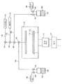
連続的な方法でパルス状に弁を開くコンピュータ制御下の空圧弁を有する図4に示す構成のチャンバを、作動した。チャンバには、Ti(NMe2)4とHf(OC(CH3)3)4(マサチューセッツ州ニューベリーポート市のストレム・ケミカル社)を収容している2つの槽がつながっていた。基板は一番上の層としてドープしたポリシリコンを有するシリコンウエハーであり、堆積に備えて150℃に維持された。
Claims (20)
- 基板を準備すること、
式M1 q(O)x(OR1)y(式I)で表される少なくとも1の前駆体化合物と式M2(NR2)w(NR3R4)z(式II)で表される少なくとも1の前駆体化合物を供給すること、
および蒸着法を用いて、前記両前駆体化合物を前記基板上に接触させることにより、金属酸化物層を形成することを含む、基板上に金属酸化物層を形成する方法であって、
前記蒸着法は、複数の堆積サイクルを含む原子層堆積法である方法;
前記式において、
M1およびM2は同じ金属であり、
それぞれのR1は互いに独立して有機基であり、
R2、R3、およびR4はそれぞれ互いに独立して水素または有機基であり、
xは0から4であり、
yは1から8であり、
wは0から4であり、
zは1から8であり、
qは1または2であり、
x、y、z、およびwは、M1およびM2の酸化状態に依存する。 - 前記基板はシリコンウエハーである、請求項1に記載の方法。
- 前記金属酸化物層は誘電体層である、請求項1又は2に記載の方法。
- 前記式において、M1およびM2 は、3、4、5、6、7、13、14族、およびランタノイドからなる金属の群から選択される、請求項1〜3の何れか一項に記載の方法。
- 前記式において、M1およびM2 は、Y、La、Pr、Nd、Gd、Ti、Zr、Hf、Nb、Ta、Si、およびAlからなる金属の群から選択される、請求項4に記載の方法。
- 前記金属酸化物層の厚さは30Åから80Åである、請求項1〜5の何れか一項に記載の方法。
- 前記式において、それぞれのR1は互いに独立して(C1〜C6)有機基であり、R2、R3、およびR4はそれぞれ互いに独立して水素または(C1〜C6)有機基である、請求項1〜6の何れか一項に記載の方法。
- 前記式において、xは0から2であり、yは2から6である、請求項1〜7の何れか一項に記載の方法。
- 前記式において、wは0から2であり、zは2から6である、請求項1〜8の何れか一項に記載の方法。
- 前記両前駆体化合物は不活性のキャリアガスの存在下で気化される、請求項1〜9の何れか一項に記載の方法。
- 前記金属酸化物層は、原子層堆積法中のそれぞれの堆積サイクル中に、前記両前駆体化合物を交互に導入することにより形成される、請求項1〜10の何れか一項に記載の方法。
- 前記基板の温度は、25℃から400℃である、請求項1〜11の何れか一項に記載の方法。
- 前記基板は、圧力が10 -4 トールから1トールの堆積チャンバ内にある、請求項1〜12の何れか一項に記載の方法。
- 請求項1〜13の何れか一項に記載の方法を用いて基板上に金属酸化物層を形成することを含む、半導体構造の製造方法であって、前記基板は半導体基板または基板アセンブリである方法。
- 前記半導体基板または基板アセンブリはシリコンウエハーである、請求項14に記載の方法。
- 前記半導体基板または基板アセンブリは堆積チャンバ内にあり、
前記方法は、前記両前駆体化合物を気化することにより、気化した両前駆体化合物を形成すること、
および前記気化した両前駆体化合物を、前記半導体基板または基板アセンブリに供給することにより、該半導体基板または基板アセンブリの1または2以上の表面上に金属酸化物の誘電体層を形成することを含む、請求項14又は15に記載の方法。 - 請求項1〜13の何れか一項に記載の方法を用いて基板上に金属酸化物層を形成することを含む、メモリデバイス構造の製造方法であって、前記基板はその上に第1の電極を有し、
前記方法は、前記両前駆体化合物を気化することにより、気化した両前駆体化合物を形成すること、
該気化した両前駆体化合物を、前記基板に供給することにより、該基板の前記第1の電極上に金属酸化物の誘電体層を形成すること、
および該誘電体層上に第2の電極を形成することを含む方法。 - 内部に基板を配置した蒸着チャンバと、
式M1 q(O)x(OR1)y(式I)で表される1または2以上の前駆体化合物を含む1または2以上の容器と、
式M2(NR2)w(NR3R4)z(式II)で表される1または2以上の前駆体化合物を含む1または2以上の容器を備える蒸着装置であって、
前記前駆体化合物の気化および供給は、複数の堆積サイクルを含む原子層堆積法を用いて達成される装置;
前記式において、
M1およびM2は同じ金属であり、
それぞれのR1は互いに独立して有機基であり、
R2、R3、およびR4はそれぞれ互いに独立して水素または有機基であり、
xは0から4であり、
yは1から8であり、
wは0から4であり、
zは1から8であり、
qは1または2であり、
x、y、z、およびwは、M1およびM2の酸化状態に依存する。 - 前記基板はシリコンウエハーである、請求項18に記載の装置。
- 前記前駆体を前記蒸着チャンバへと移動させる不活性のキャリアガスの1または2以上の発生源をさらに備える、請求項18又は19に記載の装置。
Applications Claiming Priority (2)
| Application Number | Priority Date | Filing Date | Title |
|---|---|---|---|
| US10/229,627 US6958300B2 (en) | 2002-08-28 | 2002-08-28 | Systems and methods for forming metal oxides using metal organo-amines and metal organo-oxides |
| PCT/US2003/026789 WO2004020689A2 (en) | 2002-08-28 | 2003-08-27 | Systems and methods for forming metal oxides using metal organo-amines and metal organo-oxides |
Publications (3)
| Publication Number | Publication Date |
|---|---|
| JP2005537638A JP2005537638A (ja) | 2005-12-08 |
| JP2005537638A5 JP2005537638A5 (ja) | 2006-10-05 |
| JP4355656B2 true JP4355656B2 (ja) | 2009-11-04 |
Family
ID=31976278
Family Applications (1)
| Application Number | Title | Priority Date | Filing Date |
|---|---|---|---|
| JP2004531530A Expired - Lifetime JP4355656B2 (ja) | 2002-08-28 | 2003-08-27 | 金属有機アミンと金属有機酸化物を用いて金属酸化物を形成するシステムおよび方法 |
Country Status (8)
| Country | Link |
|---|---|
| US (2) | US6958300B2 (ja) |
| EP (1) | EP1532291B1 (ja) |
| JP (1) | JP4355656B2 (ja) |
| KR (1) | KR20050043926A (ja) |
| CN (1) | CN1688743A (ja) |
| AU (1) | AU2003262900A1 (ja) |
| TW (1) | TWI270579B (ja) |
| WO (1) | WO2004020689A2 (ja) |
Families Citing this family (98)
| Publication number | Priority date | Publication date | Assignee | Title |
|---|---|---|---|---|
| US6974766B1 (en) * | 1998-10-01 | 2005-12-13 | Applied Materials, Inc. | In situ deposition of a low κ dielectric layer, barrier layer, etch stop, and anti-reflective coating for damascene application |
| US6620723B1 (en) | 2000-06-27 | 2003-09-16 | Applied Materials, Inc. | Formation of boride barrier layers using chemisorption techniques |
| US7101795B1 (en) | 2000-06-28 | 2006-09-05 | Applied Materials, Inc. | Method and apparatus for depositing refractory metal layers employing sequential deposition techniques to form a nucleation layer |
| US6551929B1 (en) | 2000-06-28 | 2003-04-22 | Applied Materials, Inc. | Bifurcated deposition process for depositing refractory metal layers employing atomic layer deposition and chemical vapor deposition techniques |
| US7405158B2 (en) | 2000-06-28 | 2008-07-29 | Applied Materials, Inc. | Methods for depositing tungsten layers employing atomic layer deposition techniques |
| US6596643B2 (en) * | 2001-05-07 | 2003-07-22 | Applied Materials, Inc. | CVD TiSiN barrier for copper integration |
| JP2005504885A (ja) | 2001-07-25 | 2005-02-17 | アプライド マテリアルズ インコーポレイテッド | 新規なスパッタ堆積方法を使用したバリア形成 |
| US9051641B2 (en) | 2001-07-25 | 2015-06-09 | Applied Materials, Inc. | Cobalt deposition on barrier surfaces |
| US20090004850A1 (en) | 2001-07-25 | 2009-01-01 | Seshadri Ganguli | Process for forming cobalt and cobalt silicide materials in tungsten contact applications |
| US8110489B2 (en) | 2001-07-25 | 2012-02-07 | Applied Materials, Inc. | Process for forming cobalt-containing materials |
| US20030029715A1 (en) | 2001-07-25 | 2003-02-13 | Applied Materials, Inc. | An Apparatus For Annealing Substrates In Physical Vapor Deposition Systems |
| US7049226B2 (en) * | 2001-09-26 | 2006-05-23 | Applied Materials, Inc. | Integration of ALD tantalum nitride for copper metallization |
| US20030059538A1 (en) * | 2001-09-26 | 2003-03-27 | Applied Materials, Inc. | Integration of barrier layer and seed layer |
| US6936906B2 (en) | 2001-09-26 | 2005-08-30 | Applied Materials, Inc. | Integration of barrier layer and seed layer |
| US6916398B2 (en) | 2001-10-26 | 2005-07-12 | Applied Materials, Inc. | Gas delivery apparatus and method for atomic layer deposition |
| US7081271B2 (en) | 2001-12-07 | 2006-07-25 | Applied Materials, Inc. | Cyclical deposition of refractory metal silicon nitride |
| WO2003065424A2 (en) * | 2002-01-25 | 2003-08-07 | Applied Materials, Inc. | Apparatus for cyclical deposition of thin films |
| US6911391B2 (en) | 2002-01-26 | 2005-06-28 | Applied Materials, Inc. | Integration of titanium and titanium nitride layers |
| US6833161B2 (en) | 2002-02-26 | 2004-12-21 | Applied Materials, Inc. | Cyclical deposition of tungsten nitride for metal oxide gate electrode |
| US6846516B2 (en) * | 2002-04-08 | 2005-01-25 | Applied Materials, Inc. | Multiple precursor cyclical deposition system |
| US7279432B2 (en) | 2002-04-16 | 2007-10-09 | Applied Materials, Inc. | System and method for forming an integrated barrier layer |
| US20030235961A1 (en) * | 2002-04-17 | 2003-12-25 | Applied Materials, Inc. | Cyclical sequential deposition of multicomponent films |
| WO2003089682A1 (en) * | 2002-04-19 | 2003-10-30 | Mattson Technology, Inc. | System for depositing a film onto a substrate using a low vapor pressure gas precursor |
| US7160577B2 (en) | 2002-05-02 | 2007-01-09 | Micron Technology, Inc. | Methods for atomic-layer deposition of aluminum oxides in integrated circuits |
| US20030232501A1 (en) * | 2002-06-14 | 2003-12-18 | Kher Shreyas S. | Surface pre-treatment for enhancement of nucleation of high dielectric constant materials |
| US6858547B2 (en) * | 2002-06-14 | 2005-02-22 | Applied Materials, Inc. | System and method for forming a gate dielectric |
| US7067439B2 (en) * | 2002-06-14 | 2006-06-27 | Applied Materials, Inc. | ALD metal oxide deposition process using direct oxidation |
| US6984592B2 (en) * | 2002-08-28 | 2006-01-10 | Micron Technology, Inc. | Systems and methods for forming metal-doped alumina |
| US7253122B2 (en) * | 2002-08-28 | 2007-08-07 | Micron Technology, Inc. | Systems and methods for forming metal oxides using metal diketonates and/or ketoimines |
| US7041609B2 (en) * | 2002-08-28 | 2006-05-09 | Micron Technology, Inc. | Systems and methods for forming metal oxides using alcohols |
| US6958300B2 (en) | 2002-08-28 | 2005-10-25 | Micron Technology, Inc. | Systems and methods for forming metal oxides using metal organo-amines and metal organo-oxides |
| US7112485B2 (en) | 2002-08-28 | 2006-09-26 | Micron Technology, Inc. | Systems and methods for forming zirconium and/or hafnium-containing layers |
| US7087481B2 (en) * | 2002-08-28 | 2006-08-08 | Micron Technology, Inc. | Systems and methods for forming metal oxides using metal compounds containing aminosilane ligands |
| US6958302B2 (en) * | 2002-12-04 | 2005-10-25 | Micron Technology, Inc. | Atomic layer deposited Zr-Sn-Ti-O films using TiI4 |
| US7101813B2 (en) | 2002-12-04 | 2006-09-05 | Micron Technology Inc. | Atomic layer deposited Zr-Sn-Ti-O films |
| US7244683B2 (en) * | 2003-01-07 | 2007-07-17 | Applied Materials, Inc. | Integration of ALD/CVD barriers with porous low k materials |
| FR2850282B1 (fr) | 2003-01-27 | 2007-04-06 | Jerome Asius | Implant injectable a base de ceramique pour le comblement de rides, depressions cutanees et cicatrices, et sa preparation |
| US7135369B2 (en) | 2003-03-31 | 2006-11-14 | Micron Technology, Inc. | Atomic layer deposited ZrAlxOy dielectric layers including Zr4AlO9 |
| US20040198069A1 (en) * | 2003-04-04 | 2004-10-07 | Applied Materials, Inc. | Method for hafnium nitride deposition |
| US7211508B2 (en) | 2003-06-18 | 2007-05-01 | Applied Materials, Inc. | Atomic layer deposition of tantalum based barrier materials |
| US7390535B2 (en) | 2003-07-03 | 2008-06-24 | Aeromet Technologies, Inc. | Simple chemical vapor deposition system and methods for depositing multiple-metal aluminide coatings |
| FR2869325B1 (fr) * | 2004-04-27 | 2006-06-16 | Commissariat Energie Atomique | Procede de depot d'une couche mince sur une couche oxydee d'un substrat |
| US20050252449A1 (en) | 2004-05-12 | 2005-11-17 | Nguyen Son T | Control of gas flow and delivery to suppress the formation of particles in an MOCVD/ALD system |
| US20060019033A1 (en) * | 2004-05-21 | 2006-01-26 | Applied Materials, Inc. | Plasma treatment of hafnium-containing materials |
| US8323754B2 (en) * | 2004-05-21 | 2012-12-04 | Applied Materials, Inc. | Stabilization of high-k dielectric materials |
| US8119210B2 (en) | 2004-05-21 | 2012-02-21 | Applied Materials, Inc. | Formation of a silicon oxynitride layer on a high-k dielectric material |
| US20060062917A1 (en) * | 2004-05-21 | 2006-03-23 | Shankar Muthukrishnan | Vapor deposition of hafnium silicate materials with tris(dimethylamino)silane |
| US7601649B2 (en) * | 2004-08-02 | 2009-10-13 | Micron Technology, Inc. | Zirconium-doped tantalum oxide films |
| US7482037B2 (en) * | 2004-08-20 | 2009-01-27 | Micron Technology, Inc. | Methods for forming niobium and/or vanadium containing layers using atomic layer deposition |
| US7588988B2 (en) | 2004-08-31 | 2009-09-15 | Micron Technology, Inc. | Method of forming apparatus having oxide films formed using atomic layer deposition |
| US7494939B2 (en) | 2004-08-31 | 2009-02-24 | Micron Technology, Inc. | Methods for forming a lanthanum-metal oxide dielectric layer |
| US7429402B2 (en) * | 2004-12-10 | 2008-09-30 | Applied Materials, Inc. | Ruthenium as an underlayer for tungsten film deposition |
| US7235501B2 (en) | 2004-12-13 | 2007-06-26 | Micron Technology, Inc. | Lanthanum hafnium oxide dielectrics |
| US7560395B2 (en) * | 2005-01-05 | 2009-07-14 | Micron Technology, Inc. | Atomic layer deposited hafnium tantalum oxide dielectrics |
| US7687409B2 (en) | 2005-03-29 | 2010-03-30 | Micron Technology, Inc. | Atomic layer deposited titanium silicon oxide films |
| US7390756B2 (en) * | 2005-04-28 | 2008-06-24 | Micron Technology, Inc. | Atomic layer deposited zirconium silicon oxide films |
| US7662729B2 (en) | 2005-04-28 | 2010-02-16 | Micron Technology, Inc. | Atomic layer deposition of a ruthenium layer to a lanthanide oxide dielectric layer |
| US7572695B2 (en) | 2005-05-27 | 2009-08-11 | Micron Technology, Inc. | Hafnium titanium oxide films |
| US7510983B2 (en) * | 2005-06-14 | 2009-03-31 | Micron Technology, Inc. | Iridium/zirconium oxide structure |
| US20070049043A1 (en) * | 2005-08-23 | 2007-03-01 | Applied Materials, Inc. | Nitrogen profile engineering in HI-K nitridation for device performance enhancement and reliability improvement |
| US7402534B2 (en) * | 2005-08-26 | 2008-07-22 | Applied Materials, Inc. | Pretreatment processes within a batch ALD reactor |
| US20070049023A1 (en) * | 2005-08-29 | 2007-03-01 | Micron Technology, Inc. | Zirconium-doped gadolinium oxide films |
| US7393736B2 (en) * | 2005-08-29 | 2008-07-01 | Micron Technology, Inc. | Atomic layer deposition of Zrx Hfy Sn1-x-y O2 films as high k gate dielectrics |
| US7410910B2 (en) | 2005-08-31 | 2008-08-12 | Micron Technology, Inc. | Lanthanum aluminum oxynitride dielectric films |
| KR101019293B1 (ko) * | 2005-11-04 | 2011-03-07 | 어플라이드 머티어리얼스, 인코포레이티드 | 플라즈마-강화 원자층 증착 장치 및 방법 |
| US7615438B2 (en) | 2005-12-08 | 2009-11-10 | Micron Technology, Inc. | Lanthanide yttrium aluminum oxide dielectric films |
| US7592251B2 (en) | 2005-12-08 | 2009-09-22 | Micron Technology, Inc. | Hafnium tantalum titanium oxide films |
| US7972974B2 (en) * | 2006-01-10 | 2011-07-05 | Micron Technology, Inc. | Gallium lanthanide oxide films |
| US7709402B2 (en) | 2006-02-16 | 2010-05-04 | Micron Technology, Inc. | Conductive layers for hafnium silicon oxynitride films |
| US7964514B2 (en) * | 2006-03-02 | 2011-06-21 | Applied Materials, Inc. | Multiple nitrogen plasma treatments for thin SiON dielectrics |
| US7582161B2 (en) | 2006-04-07 | 2009-09-01 | Micron Technology, Inc. | Atomic layer deposited titanium-doped indium oxide films |
| US7798096B2 (en) | 2006-05-05 | 2010-09-21 | Applied Materials, Inc. | Plasma, UV and ion/neutral assisted ALD or CVD in a batch tool |
| US7727908B2 (en) * | 2006-08-03 | 2010-06-01 | Micron Technology, Inc. | Deposition of ZrA1ON films |
| US7582549B2 (en) | 2006-08-25 | 2009-09-01 | Micron Technology, Inc. | Atomic layer deposited barium strontium titanium oxide films |
| US7776765B2 (en) | 2006-08-31 | 2010-08-17 | Micron Technology, Inc. | Tantalum silicon oxynitride high-k dielectrics and metal gates |
| US7544604B2 (en) * | 2006-08-31 | 2009-06-09 | Micron Technology, Inc. | Tantalum lanthanide oxynitride films |
| US7605030B2 (en) | 2006-08-31 | 2009-10-20 | Micron Technology, Inc. | Hafnium tantalum oxynitride high-k dielectric and metal gates |
| US20080057659A1 (en) * | 2006-08-31 | 2008-03-06 | Micron Technology, Inc. | Hafnium aluminium oxynitride high-K dielectric and metal gates |
| US7759747B2 (en) * | 2006-08-31 | 2010-07-20 | Micron Technology, Inc. | Tantalum aluminum oxynitride high-κ dielectric |
| US7563730B2 (en) * | 2006-08-31 | 2009-07-21 | Micron Technology, Inc. | Hafnium lanthanide oxynitride films |
| US7521379B2 (en) * | 2006-10-09 | 2009-04-21 | Applied Materials, Inc. | Deposition and densification process for titanium nitride barrier layers |
| KR100829539B1 (ko) * | 2007-04-13 | 2008-05-16 | 삼성전자주식회사 | 박막 제조 방법, 이를 이용한 게이트 구조물 및 커패시터의제조 방법 |
| KR100888617B1 (ko) * | 2007-06-15 | 2009-03-17 | 삼성전자주식회사 | 상변화 메모리 장치 및 그 형성 방법 |
| US7659158B2 (en) | 2008-03-31 | 2010-02-09 | Applied Materials, Inc. | Atomic layer deposition processes for non-volatile memory devices |
| US20100062149A1 (en) * | 2008-09-08 | 2010-03-11 | Applied Materials, Inc. | Method for tuning a deposition rate during an atomic layer deposition process |
| US8491967B2 (en) | 2008-09-08 | 2013-07-23 | Applied Materials, Inc. | In-situ chamber treatment and deposition process |
| US8907059B2 (en) * | 2008-11-14 | 2014-12-09 | Bio-Rad Laboratories, Inc. | Phosphopeptide enrichment of compositions by fractionation on ceramic hydroxyapatite |
| DE102009028801B3 (de) * | 2009-08-21 | 2011-04-14 | Evonik Degussa Gmbh | Verfahren zur Herstellung Indiumoxid-haltiger Schichten, nach dem Verfahren herstellbare Indiumoxid-haltige Schicht und deren Verwendung |
| DE102009028802B3 (de) * | 2009-08-21 | 2011-03-24 | Evonik Degussa Gmbh | Verfahren zur Herstellung Metalloxid-haltiger Schichten, nach dem Verfahren herstellbare Metalloxid-haltige Schicht und deren Verwendung |
| DE102010031592A1 (de) * | 2010-07-21 | 2012-01-26 | Evonik Degussa Gmbh | Indiumoxoalkoxide für die Herstellung Indiumoxid-haltiger Schichten |
| DE102010031895A1 (de) | 2010-07-21 | 2012-01-26 | Evonik Degussa Gmbh | Indiumoxoalkoxide für die Herstellung Indiumoxid-haltiger Schichten |
| DE102012209918A1 (de) | 2012-06-13 | 2013-12-19 | Evonik Industries Ag | Verfahren zur Herstellung Indiumoxid-haltiger Schichten |
| KR101953893B1 (ko) * | 2012-11-08 | 2019-03-06 | 주식회사 원익아이피에스 | 산화물 반도체 박막의 형성방법 및 형성장치 |
| EP3410208A1 (en) | 2017-06-01 | 2018-12-05 | Evonik Degussa GmbH | Device containing metal oxide-containing layers |
| EP3409813A1 (en) | 2017-06-01 | 2018-12-05 | Evonik Degussa GmbH | Device containing metal oxide-containing layers |
| US10319588B2 (en) * | 2017-10-10 | 2019-06-11 | Asm Ip Holding B.V. | Method for depositing a metal chalcogenide on a substrate by cyclical deposition |
| JP7413258B2 (ja) | 2017-11-19 | 2024-01-15 | アプライド マテリアルズ インコーポレイテッド | 金属表面上の金属酸化物のaldのための方法 |
| JP7587873B2 (ja) * | 2022-05-10 | 2024-11-21 | イージーティーエム カンパニー リミテッド | 薄膜形成方法およびそれを含むメモリ素子の製造方法 |
Family Cites Families (47)
| Publication number | Priority date | Publication date | Assignee | Title |
|---|---|---|---|---|
| US70126A (en) * | 1867-10-22 | Benjamin franklin shbeman | ||
| US40501A (en) * | 1863-11-03 | Improved machine for grinding ores and amalgamating precious metals | ||
| US213987A (en) * | 1879-04-08 | Improvement in bevels | ||
| US43149A (en) * | 1864-06-14 | Improvement in calisthenic pulleys and spring-cords | ||
| US175393A (en) * | 1876-03-28 | Improvement in molds for casting stereotype-plates | ||
| US46197A (en) * | 1865-01-31 | Improvement in the manufacture of molded candles | ||
| US54213A (en) * | 1866-04-24 | Improvement in hay and straw stackers | ||
| US43632A (en) * | 1864-07-26 | Improvement in churns | ||
| KR930012120B1 (ko) * | 1991-07-03 | 1993-12-24 | 삼성전자 주식회사 | 반도체장치 및 그의 제조방법 |
| JPH05239650A (ja) | 1992-02-27 | 1993-09-17 | Kojundo Chem Lab Co Ltd | シリコン酸化膜の製造法 |
| JP3407409B2 (ja) * | 1994-07-27 | 2003-05-19 | 富士通株式会社 | 高誘電率薄膜の製造方法 |
| US6313035B1 (en) * | 1996-05-31 | 2001-11-06 | Micron Technology, Inc. | Chemical vapor deposition using organometallic precursors |
| US6011123A (en) * | 1996-11-20 | 2000-01-04 | Jsr Corporation | Curable resin composition and cured products |
| US6303391B1 (en) * | 1997-06-26 | 2001-10-16 | Advanced Technology Materials, Inc. | Low temperature chemical vapor deposition process for forming bismuth-containing ceramic films useful in ferroelectric memory devices |
| US6013553A (en) | 1997-07-24 | 2000-01-11 | Texas Instruments Incorporated | Zirconium and/or hafnium oxynitride gate dielectric |
| US7157385B2 (en) * | 2003-09-05 | 2007-01-02 | Micron Technology, Inc. | Method of depositing a silicon dioxide-comprising layer in the fabrication of integrated circuitry |
| US6093944A (en) * | 1998-06-04 | 2000-07-25 | Lucent Technologies Inc. | Dielectric materials of amorphous compositions of TI-O2 doped with rare earth elements and devices employing same |
| JP4152028B2 (ja) * | 1999-01-25 | 2008-09-17 | 株式会社Adeka | ルテニウム系薄膜の製造方法 |
| US6312831B1 (en) | 1999-04-30 | 2001-11-06 | Visteon Global Technologies, Inc. | Highly reflective, durable titanium/tin oxide films |
| US6273951B1 (en) | 1999-06-16 | 2001-08-14 | Micron Technology, Inc. | Precursor mixtures for use in preparing layers on substrates |
| US6060755A (en) | 1999-07-19 | 2000-05-09 | Sharp Laboratories Of America, Inc. | Aluminum-doped zirconium dielectric film transistor structure and deposition method for same |
| US6221712B1 (en) * | 1999-08-30 | 2001-04-24 | United Microelectronics Corp. | Method for fabricating gate oxide layer |
| JP2001108199A (ja) | 1999-10-12 | 2001-04-20 | Tori Chemical Kenkyusho:Kk | 残留物のパージが簡易な流体移送用配管装置及び流体供給装置、並びに配管装置中の残留物をパージする方法及び流体供給方法。 |
| US6203613B1 (en) | 1999-10-19 | 2001-03-20 | International Business Machines Corporation | Atomic layer deposition with nitrate containing precursors |
| US6780704B1 (en) | 1999-12-03 | 2004-08-24 | Asm International Nv | Conformal thin films over textured capacitor electrodes |
| US6335049B1 (en) | 2000-01-03 | 2002-01-01 | Micron Technology, Inc. | Chemical vapor deposition methods of forming a high K dielectric layer and methods of forming a capacitor |
| KR100803770B1 (ko) * | 2000-03-07 | 2008-02-15 | 에이에스엠 인터내셔널 엔.브이. | 구배(graded)박막 |
| JP2001257344A (ja) | 2000-03-10 | 2001-09-21 | Toshiba Corp | 半導体装置及び半導体装置の製造方法 |
| GB0007361D0 (en) | 2000-03-28 | 2000-05-17 | Ncr Int Inc | Self-service terminal |
| US6984591B1 (en) | 2000-04-20 | 2006-01-10 | International Business Machines Corporation | Precursor source mixtures |
| KR20010114050A (ko) * | 2000-06-20 | 2001-12-29 | 박종섭 | 반도체 소자의 알루미늄 산화막 형성 방법 |
| US6837251B1 (en) | 2000-06-21 | 2005-01-04 | Air Products And Chemicals, Inc. | Multiple contents container assembly for ultrapure solvent purging |
| US6969539B2 (en) | 2000-09-28 | 2005-11-29 | President And Fellows Of Harvard College | Vapor deposition of metal oxides, silicates and phosphates, and silicon dioxide |
| TW486392B (en) * | 2000-09-29 | 2002-05-11 | Air Prod & Chem | Solvent blend for use in high purity precursor removal |
| US6300203B1 (en) | 2000-10-05 | 2001-10-09 | Advanced Micro Devices, Inc. | Electrolytic deposition of dielectric precursor materials for use in in-laid gate MOS transistors |
| KR100385952B1 (ko) * | 2001-01-19 | 2003-06-02 | 삼성전자주식회사 | 탄탈륨 산화막을 가진 반도체 커패시터 및 그의 제조방법 |
| US6586792B2 (en) * | 2001-03-15 | 2003-07-01 | Micron Technology, Inc. | Structures, methods, and systems for ferroelectric memory transistors |
| US6541280B2 (en) * | 2001-03-20 | 2003-04-01 | Motorola, Inc. | High K dielectric film |
| DE10296448T5 (de) * | 2001-03-20 | 2004-04-15 | Mattson Technology Inc., Fremont | Verfahren zum Abscheiden einer Schicht mit einer verhältnismässig hohen Dielektrizitätskonstante auf ein Substrat |
| US7005392B2 (en) * | 2001-03-30 | 2006-02-28 | Advanced Technology Materials, Inc. | Source reagent compositions for CVD formation of gate dielectric thin films using amide precursors and method of using same |
| KR100418569B1 (ko) * | 2001-12-10 | 2004-02-14 | 주식회사 하이닉스반도체 | 단원자층증착을 이용한 고유전체 박막 형성방법 |
| US7164165B2 (en) * | 2002-05-16 | 2007-01-16 | Micron Technology, Inc. | MIS capacitor |
| JP3627106B2 (ja) | 2002-05-27 | 2005-03-09 | 株式会社高純度化学研究所 | 原子層吸着堆積法によるハフニウムシリケート薄膜の製造方法 |
| US6958300B2 (en) * | 2002-08-28 | 2005-10-25 | Micron Technology, Inc. | Systems and methods for forming metal oxides using metal organo-amines and metal organo-oxides |
| US7112485B2 (en) * | 2002-08-28 | 2006-09-26 | Micron Technology, Inc. | Systems and methods for forming zirconium and/or hafnium-containing layers |
| US7041609B2 (en) | 2002-08-28 | 2006-05-09 | Micron Technology, Inc. | Systems and methods for forming metal oxides using alcohols |
| US20050070126A1 (en) * | 2003-04-21 | 2005-03-31 | Yoshihide Senzaki | System and method for forming multi-component dielectric films |
-
2002
- 2002-08-28 US US10/229,627 patent/US6958300B2/en not_active Expired - Lifetime
-
2003
- 2003-08-27 KR KR1020057003579A patent/KR20050043926A/ko not_active Ceased
- 2003-08-27 CN CNA038245825A patent/CN1688743A/zh active Pending
- 2003-08-27 AU AU2003262900A patent/AU2003262900A1/en not_active Abandoned
- 2003-08-27 TW TW092123623A patent/TWI270579B/zh not_active IP Right Cessation
- 2003-08-27 JP JP2004531530A patent/JP4355656B2/ja not_active Expired - Lifetime
- 2003-08-27 WO PCT/US2003/026789 patent/WO2004020689A2/en not_active Ceased
- 2003-08-27 EP EP03791827.3A patent/EP1532291B1/en not_active Expired - Lifetime
-
2005
- 2005-08-31 US US11/216,629 patent/US20050287819A1/en not_active Abandoned
Also Published As
| Publication number | Publication date |
|---|---|
| AU2003262900A8 (en) | 2004-03-19 |
| WO2004020689A2 (en) | 2004-03-11 |
| EP1532291B1 (en) | 2014-09-24 |
| US6958300B2 (en) | 2005-10-25 |
| TWI270579B (en) | 2007-01-11 |
| WO2004020689A3 (en) | 2004-06-17 |
| US20050287819A1 (en) | 2005-12-29 |
| TW200406502A (en) | 2004-05-01 |
| CN1688743A (zh) | 2005-10-26 |
| EP1532291A2 (en) | 2005-05-25 |
| JP2005537638A (ja) | 2005-12-08 |
| KR20050043926A (ko) | 2005-05-11 |
| AU2003262900A1 (en) | 2004-03-19 |
| WO2004020689A8 (en) | 2004-11-25 |
| US20040043630A1 (en) | 2004-03-04 |
Similar Documents
| Publication | Publication Date | Title |
|---|---|---|
| JP4355656B2 (ja) | 金属有機アミンと金属有機酸化物を用いて金属酸化物を形成するシステムおよび方法 | |
| US7410918B2 (en) | Systems and methods for forming metal oxides using alcohols | |
| US7576378B2 (en) | Systems and methods for forming metal oxides using metal diketonates and/or ketoimines | |
| US6984592B2 (en) | Systems and methods for forming metal-doped alumina | |
| US7482284B2 (en) | Deposition methods for forming silicon oxide layers | |
| US7300873B2 (en) | Systems and methods for forming metal-containing layers using vapor deposition processes | |
| US20050160981A9 (en) | Systems and methods for forming zirconium and/or hafnium-containing layers |
Legal Events
| Date | Code | Title | Description |
|---|---|---|---|
| A521 | Request for written amendment filed |
Free format text: JAPANESE INTERMEDIATE CODE: A523 Effective date: 20060821 |
|
| A621 | Written request for application examination |
Free format text: JAPANESE INTERMEDIATE CODE: A621 Effective date: 20060821 |
|
| A977 | Report on retrieval |
Free format text: JAPANESE INTERMEDIATE CODE: A971007 Effective date: 20090626 |
|
| TRDD | Decision of grant or rejection written | ||
| A01 | Written decision to grant a patent or to grant a registration (utility model) |
Free format text: JAPANESE INTERMEDIATE CODE: A01 Effective date: 20090707 |
|
| A01 | Written decision to grant a patent or to grant a registration (utility model) |
Free format text: JAPANESE INTERMEDIATE CODE: A01 |
|
| A61 | First payment of annual fees (during grant procedure) |
Free format text: JAPANESE INTERMEDIATE CODE: A61 Effective date: 20090803 |
|
| R150 | Certificate of patent or registration of utility model |
Ref document number: 4355656 Country of ref document: JP Free format text: JAPANESE INTERMEDIATE CODE: R150 Free format text: JAPANESE INTERMEDIATE CODE: R150 |
|
| FPAY | Renewal fee payment (event date is renewal date of database) |
Free format text: PAYMENT UNTIL: 20120807 Year of fee payment: 3 |
|
| FPAY | Renewal fee payment (event date is renewal date of database) |
Free format text: PAYMENT UNTIL: 20130807 Year of fee payment: 4 |
|
| R250 | Receipt of annual fees |
Free format text: JAPANESE INTERMEDIATE CODE: R250 |
|
| R250 | Receipt of annual fees |
Free format text: JAPANESE INTERMEDIATE CODE: R250 |
|
| R250 | Receipt of annual fees |
Free format text: JAPANESE INTERMEDIATE CODE: R250 |
|
| R250 | Receipt of annual fees |
Free format text: JAPANESE INTERMEDIATE CODE: R250 |
|
| R250 | Receipt of annual fees |
Free format text: JAPANESE INTERMEDIATE CODE: R250 |
|
| R250 | Receipt of annual fees |
Free format text: JAPANESE INTERMEDIATE CODE: R250 |
|
| R250 | Receipt of annual fees |
Free format text: JAPANESE INTERMEDIATE CODE: R250 |
|
| R250 | Receipt of annual fees |
Free format text: JAPANESE INTERMEDIATE CODE: R250 |
|
| R250 | Receipt of annual fees |
Free format text: JAPANESE INTERMEDIATE CODE: R250 |
|
| R250 | Receipt of annual fees |
Free format text: JAPANESE INTERMEDIATE CODE: R250 |
|
| R250 | Receipt of annual fees |
Free format text: JAPANESE INTERMEDIATE CODE: R250 |
|
| R250 | Receipt of annual fees |
Free format text: JAPANESE INTERMEDIATE CODE: R250 |
|
| EXPY | Cancellation because of completion of term |