JP4360077B2 - Manufacturing method of semiconductor device - Google Patents
Manufacturing method of semiconductor device Download PDFInfo
- Publication number
- JP4360077B2 JP4360077B2 JP2002302137A JP2002302137A JP4360077B2 JP 4360077 B2 JP4360077 B2 JP 4360077B2 JP 2002302137 A JP2002302137 A JP 2002302137A JP 2002302137 A JP2002302137 A JP 2002302137A JP 4360077 B2 JP4360077 B2 JP 4360077B2
- Authority
- JP
- Japan
- Prior art keywords
- wafer
- adhesive sheet
- rigidity
- peeled
- manufacturing
- Prior art date
- Legal status (The legal status is an assumption and is not a legal conclusion. Google has not performed a legal analysis and makes no representation as to the accuracy of the status listed.)
- Expired - Fee Related
Links
Images









Landscapes
- Mechanical Treatment Of Semiconductor (AREA)
- Dicing (AREA)
Description
【0001】
【発明の属する技術分野】
本発明は、半導体素子の製造方法に関し、特に絶縁ゲート型バイポーラトランジスタ(以下、IGBTとする)等の電力用半導体素子の製造方法に関する。
【0002】
【従来の技術】
IGBTは、電圧駆動型であり、オン電圧が低く、かつ高速スイッチング特性を有する素子であり、その応用範囲も、インバータなどの産業用分野から電子レンジなどの民生機器分野へ拡がっている。従来、IGBTには、パンチスルー(以下、PTとする)型、ノンパンチスルー(以下、NPTとする)型、フィールドストップ(以下、FSとする)型の構造があり、nチャネル型の縦型二重拡散構造のものが主流である。
【0003】
PT型IGBTは、p+半導体基板上にn+バッファ層とn-活性層をエピタキシャル成長させたエピウエハーを用いて形成される。そのため、たとえば耐圧600V系の素子では、活性層の厚さは70μm程度であるが、基板を含む総厚さは200〜300μm程度になる。
【0004】
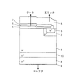
図29は、低ドーズ量の浅いp+コレクタ層を有するNPT型IGBTの1/2セル分の構成を示す断面図である。図29に示すように、たとえばFZウエハーよりなるn-半導体基板を活性層1とし、その表面側に、p+ベース領域2が選択的に形成されている。ベース領域2の表面層には、n+エミッタ領域3が選択的に形成されている。また、基板表面上には、ゲート酸化膜4を介してゲート電極5が形成されている。
【0005】
エミッタ電極6は、エミッタ領域3およびベース領域2に接触しているとともに、層間絶縁膜7によりゲート電極5から絶縁されている。基板裏面には、p+コレクタ層8およびコレクタ電極9が形成されている。NPT型の場合には、活性層1の厚さがPT型よりも厚くなるが、素子全体としては、PT型の素子に比べて、大幅に薄くなる。また、エピタキシャル基板を用いずに、FZ基板を用いているため、安価である。
【0006】
図30は、FS型IGBTの1/2セル分の構成を示す断面図である。図30に示すように、基板表面側の素子構造は、図29に示すNPT型の素子と同じである。基板裏面側には、n-活性層1とp+コレクタ層8との間に、n+バッファ層10が設けられている。FS型の場合、活性層1の厚さは、PT型と同じ70μm程度(耐圧600V系)であり、素子全体の厚さは100〜200μm程度である。
【0007】
最近では、総合損失をより低減するため、ウエハーを薄く削り、デバイス厚をできるだけ薄くする試みがなされている。たとえば、耐圧600V系の素子の場合、FS−IGBTの厚さは70μm程度が想定されている。耐圧クラスが低くなると、素子の厚さはさらに薄くなる。このような厚さのFS型IGBTまたはそれに類似したデバイスの製造方法として、以下に説明するように、FZウエハーを研磨する方法と、エピタキシャルウエハーを研磨する方法が知られている。
【0008】
図31は、従来のFZウエハーを用いたFS型IGBTの製造プロセスを示す図である。図31に示すように、まず、活性層1となるn-FZウエハーの表面側に、ベース領域、エミッタ領域、ゲート酸化膜、ゲート電極、層間絶縁膜、エミッタ電極およびパッシベーション膜よりなる表面側素子構造部11を形成する(同図(a))。ついで、ウエハーの裏面を、バックグラインド、ポリシュあるいはエッチング等の加工方法を単独または組合せて研削し、ウエハーを所望の厚さ、たとえば70μmの厚さとする(図31(b))。なお、エッチングの場合、厳密には研削ではないが、本明細書では、ウエハーを薄くする手段については問わないので、エッチングを含めて研削とする。
【0009】
ついで、ウエハーの裏面から、たとえばn型不純物であるリン(P)と、p型不純物であるボロン(B)をイオン注入し、電気炉で350〜500℃の熱処理(アニール)をおこない、バッファ層10およびコレクタ層8を形成する(図31(c))。ついで、ウエハーの裏面、すなわちコレクタ層8の表面に、アルミニウム(Al)、チタン(Ti)、ニッケル(Ni)および金(Au)などの複数の金属を蒸着し、コレクタ電極9を形成する(図31(d))。最後に、コレクタ電極9側にダイシングテープ12を貼り付けてダイシングをおこない、ウエハーを複数のチップ13に切断する(図31(e))。
【0010】
図32は、従来のエピタキシャルウエハーを用いたFS型IGBTの製造プロセスを示す図である。図32に示すように、まず、バッファ層10となるn+半導体基板上に、活性層1となるエピタキシャル層を成長させたエピタキシャルウエハーを用意し、そのエピタキシャル層側の表面に、ベース領域、エミッタ領域、ゲート酸化膜、ゲート電極、層間絶縁膜、エミッタ電極およびパッシベーション膜よりなる表面側素子構造部11を形成する(同図(a))。表面側素子構造部11を形成時の拡散工程においてn層が拡散していく。ついで、バックグラインド等により、ウエハーをたとえば70μmの厚さにし、n+半導体基板がたとえば10μmの厚さで残るようにする(図32(b))。
【0011】
ついで、ウエハーの裏面から、たとえばp型不純物であるボロンをイオン注入し、電気炉で350〜500℃のアニールをおこない、コレクタ層8を形成する(図32(c))。ついで、コレクタ層8の表面に、複数の金属層よりなるコレクタ電極9を形成する(図32(d))。最後に、ダイシングテープ12を貼り付けてダイシングをおこない、ウエハーを複数のチップ13に切断する(図32(e))。
【0012】
図33は、従来のバックグラインド工程を詳細に説明するためのプロセス図である。図33に示すように、バックグラインド工程では、まず、図示しない表面側素子構造部が形成されたウエハー15の表面側に、保護テープ16を貼り付ける(同図(a))。これを裏返し、保護テープ16を下にして、バックグラインド装置の吸着台19に真空吸着させる(図33(b))。
【0013】
そして、バックグラインドをおこなう。その際、ウエハー15の表面には、パッシベーション膜を構成するポリイミドの段差部17が形成されているため、その段差部17のパターンを反映した凹部18がウエハー裏面に形成される(図33(c))。バックグラインド終了後、吸着台19からウエハー15を取り外し、保護テープ16を剥がす(図33(d))。このようにして、所望の厚さのウエハー15が得られる(図33(e))。
【0014】
【発明が解決しようとする課題】
しかしながら、上述した従来の製造方法によりたとえば70μm厚程度の素子を作製しようとすると、バックグラインド後のウエハーが薄過ぎるため、ウエハー裏面側からイオン注入をおこなう際に、ウエハーが割れやすいという問題点がある。また、ウエハー裏面にコレクタ電極となる金属膜を蒸着すると、その金属膜が、基板側からみて圧縮応力の大きな膜となるため、ウエハーに割れが生じやすいという問題点がある。
【0015】
また、電気炉によるアニール時にウエハーに発生する応力によって、ウエハーが割れやすくなるという問題点がある。また、ウエハー割れが生じなくても、圧縮応力によってウエハーが大きく反るため、ダイシングが困難になるという問題点がある。また、ダイシング後のチップの形が歪むため、設計通りの特性が得られないおそれがある。
【0016】
また、上述した従来のバックグラインド工程では、バックグラインドによってウエハー裏面が凹凸形状になり、特に真空吸着の強い箇所で深く削れてしまう(図33(e)参照、中央の凹部)ため、ウエハー割れが起こりやすいという問題点がある。また、ウエハー外周部の強度が低いため、ウエハーの外周がバックグラインド装置の吸着台から浮き上がってしまい、ウエハー割れの原因になるという問題点がある。また、ウエハー裏面が局所的に削れてしまうことによって、所望のデバイス特性が得られないおそれがある。
【0017】
本発明は、上記問題点に鑑みてなされたものであって、ウエハー裏面をバックグラインドしてデバイス厚の薄いIGBT等の半導体素子を製造するにあたって、ウエハーの反りやウエハーに作用する応力を抑制することによって、ウエハーが割れるのを防ぎながら半導体素子を作製することができる半導体素子の製造方法を提供することを目的とする。
【0018】
また、本発明は、バックグラインド時にウエハー裏面に局所的な削れが生じるのを防ぐことによって、ウエハーが割れるのを防ぐようにした半導体素子の製造方法を提供することを目的とする。
【0019】
【課題を解決するための手段】
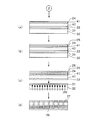
上記目的を達成するため、本発明にかかる半導体素子の製造方法は、半導体ウエハーの表面に半導体素子の表面側素子構造部を作製する工程と、前記半導体ウエハーの、前記表面側素子構造部が作製された側の面に高剛性の接着シートを貼り付ける工程と、前記高剛性の接着シートにさらにパーティクル除去用の接着シートを貼り付ける工程と、前記高剛性の接着シートおよび前記パーティクル除去用の接着シートを貼り付けた状態のまま前記半導体ウエハーの裏面を、当該半導体ウエハーの裏面側の表面が平坦になるように研削する工程と、前記パーティクル除去用の接着シートを剥離させる工程と、前記パーティクル除去用の接着シートの剥離後、イオン注入をおこない、注入された不純物をレーザーアニール法により活性化させて、前記半導体ウエハーの研削された面の表面に応力が生じないように裏面構造を作製する工程と、裏面構造が作製された前記半導体ウエハーから前記高剛性の接着シートを剥離させる工程と、前記高剛性の接着シートの剥離後、前記半導体ウエハーをチップ状に切断する工程と、を含むことを特徴とする。
【0020】
この発明において、裏面構造を作製する際に、イオン注入をおこない、注入された不純物をレーザーアニール法により活性化させる構成としてもよい。
【0023】
この発明において、前記半導体ウエハーに前記接着シートを貼り付けた後、当該接着シートにさらにパーティクル除去用の接着シートを貼り付け、ウエハー裏面の研削後、前記パーティクル除去用の接着シートを剥がしてから、裏面構造を作製する構成としてもよい。
【0024】
この発明によれば、半導体ウエハーの表面側に、半導体素子の表面側素子構造部を形成した後、その表面に高剛性接着シートを貼り付け、この状態でバックグラインドをおこなってウエハーを薄くした後、ウエハー裏面に対する処理をおこなうことにより、ウエハー裏面に対する処理をおこなっている間のウエハーの反りや、ウエハーに作用する応力が抑制される。
【0025】
また、本発明によれば、半導体ウエハーの裏面に、高剛性接着シートおよびパーティクル除去用接着シートを貼り付けた状態でバックグラインドをおこない、裏面研削終了後にパーティクル除去用接着シートを剥がしてから裏面構造の作製をおこなうことにより、ウエハー裏面の研削時に発生した削り屑やその他の塵などのパーティクルが、裏面構造を作製する前に取り除かれる。
【0030】
【発明の実施の形態】
以下に、本発明の実施の形態について図面を参照しつつ詳細に説明する。なお、実施の形態においては、本発明方法によりIGBTを製造する場合を例にして説明する。また、以下の各実施の形態の説明および添付図面では、同様の構成については同一の符号を付す。
【0031】
実施の形態1.
図1および図2は、本発明の実施の形態1にかかる半導体素子の製造方法の製造プロセスを示す図である。まず、n-FZウエハー21の表面側に、SiO2等のゲート酸化膜とポリシリコンからなるゲート電極を堆積し、これらを加工する。そして、その表面にBPSG等の層間絶縁膜を堆積し、これを加工することによって、絶縁ゲート構造を作製する。つづいて、P+ベース層を形成し、その中にn+エミッタ層を形成する。
【0032】
そして、Al−Si膜からなる表面電極、すなわちエミッタ電極を形成し、400〜500℃程度で熱処理をおこなって、Al−Si膜を安定した接合性を有する低抵抗配線とする。その上全面に、ポリイミドのパッシベーション膜を積層し、図30に示す構成と同様の表面側素子構造部22ができあがる(図1(a))。本明細書では、ウエハー21の、表面側素子構造部22が形成される側の面をウエハー表面とし、その反対側の面をウエハー裏面とする。なお、図1および図2においては、表面側素子構造部22の詳細な構成の図示を省略する。
【0033】
ついで、ウエハー21を裏返し、表面側素子構造部22の表面に、両面接着タイプの接着シート31を介して、支持基板32を接合する(図1(b))。ここでは、支持基板32として、たとえばUV光を透過する石英ガラスウエハーを用いる。また、接着シート31として、たとえばUV光の照射で接着剤が硬化することにより剥離可能な高剛性UVテープ型シートや耐熱性UVテープ型シート、あるいは加熱発泡により剥離可能な加熱発泡テープ型シートで、接着時に気泡が入らないものを用いる。接着シート31の厚さは、たとえば100μm程度であるのが適当である。また、接着シート31は、耐熱温度が高く、アウトガスが少なく、剥離しやすいものがよい。
【0034】
ついで、支持基板32を接合した状態で、ウエハー裏面をバックグラインドやエッチング等により研削し、表面側素子構造部22を含むウエハー全体の厚さを所望の厚さ、たとえば70μmとする(図1(c))。ついで、ウエハー21の裏面から、たとえばn型不純物であるリンを、ドーズ量がたとえば1×10¹¹〜1×1013cm-2で、加速電圧がたとえば200k〜6MeVでイオン注入する。つづいて、ウエハー21の裏面から、たとえばp型不純物であるボロンを、ドーズ量がたとえば1×10¹³〜1×1015cm-2で、加速電圧がたとえば20k〜100keVでイオン注入する。
【0035】
その後、ウエハー裏面にレーザーを照射してアニールをおこない、バッファ層となるn+層23およびコレクタ層となるp+層24を形成する(図2(a))。特に限定しないが、ここでは、レーザーとして、たとえばYAGの第3高調波(YAG3ω)パルスレーザー(波長:355nm、半値幅:100〜500ns、周波数:500Hz)を用いる。そして、たとえば一回の照射エリアを約1mm角とし、50%〜90%オーバーラップさせて照射する。YAGの第3高調波を用いる理由は、深いn+層23を形成することができるからである。また、このレーザーアニールによって、ウエハー裏面のp+層24およびn+層23のみを活性化させることができ、接着シート31の耐熱温度に関係なく熱処理をおこなうことができる。
【0036】
ついで、ウエハー裏面に、たとえばアルミニウム、チタン、ニッケルおよび金などの複数の金属を蒸着し、コレクタ電極となる裏面電極25を形成する(図2(b))。ここで、低温スパッタ法により金属膜の蒸着をおこなうのが適当である。その理由は、接着シート31の耐熱温度がおおよそ、高剛性UVテープ型シートでは100℃以下であり、耐熱性UVテープ型シートでは200℃以下であり、加熱発泡テープ型シートでは150℃以下であるため、成膜時の温度は100℃以下であるのが望ましいからである。
【0037】
ついで、ウエハー裏面に一般的なダイシングテープ26を貼り付ける。そして、支持基板32側からUV光を照射し、表面側素子構造部22のパッシベーション膜との界面で接着シート31を剥離させ、接着シート31および支持基板32を取り除く(図2(c))。その際、表面側素子構造部22に接着シート31の接着剤の残渣が残らないように注意する。なお、接着シート31が加熱発泡テープ型シートの場合には、UV光の照射の代わりに、加熱発泡により接着シート31を剥離させる。その後、ウエハー21を複数のチップ27に切断する(図2(d))。図示省略するが、各チップ27は、裏面電極25を介して配線基板等の固定部材に半田付けされる。そして、各チップ27のウエハー表面側の電極には、アルミワイヤ電極が超音波ワイヤボンディング装置により固着される。
【0038】
上述した実施の形態1によれば、表面側素子構造部22を形成した後、その表面に支持基板32を接合し、この状態でバックグラインドをおこなってウエハー21を薄くした後、ウエハー裏面に対する処理をおこなうので、ウエハー裏面に対する処理をおこなっている間のウエハー21の反りや、ウエハー21に作用する応力を抑制することができる。また、応力の発生源となる電気炉アニールに代えて、レーザーアニールを採用したことにより、ウエハー21に作用する応力を抑制することができる。したがって、ウエハー裏面に対する処理をおこなっている間にウエハー21が割れるのを防ぐことができる。また、ウエハー21の反りが小さくなるので、容易にダイシングをおこなうことができるとともに、設計通りのデバイス特性が得られる。また、レーザーアニールをおこなうことによって、p+層24の高濃度化が図れるので、オン電圧の低減を図ることができる。
【0039】
なお、上述した実施の形態1において、接着シート31として加熱発泡テープ型シートを用いた場合には、支持基板32は、UV光を透過させる必要がないので、金属やセラミックや硬質プラスチックなど、UV光が透過しない材質でできていてもよい。また、接着シート31は、その両面の粘着剤がUV硬化型であってもよいし、両面の粘着剤が加熱発泡型であってもよいし、支持基板32側の面および素子側の面がそれぞれUV硬化型および加熱発泡型であってもよいし、その逆でもよい。
【0040】
また、NPT型のIGBTを作製する場合には、実施の形態1において、n+層23を形成するためのn型不純物(リン)のイオン注入工程を省略すればよい。その場合、ウエハー裏面のレーザーアニールに用いるレーザーは、半値幅の短いXeFパルスレーザー(波長:351nm、半値幅:14ns)や、XeClパルスレーザー(波長:308nm、半値幅:49ns)でもよい。これらのレーザー、またはYAGの第2高調波(YAG2ω)や第3高調波(YAG3ω)パルスレーザーを用いれば、p+層24のみを活性化させることができる。
【0041】
実施の形態2.
図3および図4は、本発明の実施の形態2にかかる半導体素子の製造方法の製造プロセスを示す図である。実施の形態2では、nドープのエピタキシャルウエハーを用いる。まず、n+半導体基板41の上に、エピタキシャル層42を成長させたエピタキシャルウエハーの表面側、すなわちエピタキシャル層42の表面に、実施の形態1と同様にして、図30に示す構成と同様の表面側素子構造部22を作製する(図3(a))。この表面側素子構造部22を作製する際の拡散工程においてn層が拡散していく。なお、図3および図4においては、表面側素子構造部22の詳細な構成の図示を省略する。
【0042】
ついで、ウエハーを裏返し、表面側素子構造部22の表面に、接着シート31を介して、支持基板32を接合する(図3(b))。接着シート31および支持基板32については、実施の形態1と同じであるので、重複する説明を省略する。ただし、実施の形態2では、支持基板32の厚さは、たとえば625μmである。
【0043】
ついで、支持基板32を接合した状態で、ウエハー裏面をバックグラインドやエッチング等により研削し、表面側素子構造部22を含むウエハー全体の厚さが所望の厚さ、たとえば70μmで、かつn+半導体基板41がたとえば10μmの厚さで残るようにする(図3(c))。ついで、ウエハーの裏面から、たとえばp型不純物であるボロンを、ドーズ量がたとえば1×10¹⁴〜1×1015cm-2で、加速電圧がたとえば20k〜100keVでイオン注入する。
【0044】
その後、ウエハー裏面にレーザーを照射してアニールをおこない、コレクタ層となるp+層24を形成する(図4(a))。特に限定しないが、ここでは、レーザーとして、XeClパルスレーザー(波長:308nm、半値幅:49ns、周波数:100Hz)を用いる。そして、たとえば一回の照射エリアを約1mm角とし、50%〜90%オーバーラップさせて照射する。このレーザーアニールによって、ウエハー裏面のp+層24のみを活性化させることができ、接着シート31の耐熱温度に関係なく熱処理をおこなうことができる。なお、XeClに代えて、YAG2ω、YAG3ωやXeFを用いてもよい。
【0045】
ついで、ウエハー裏面に、実施の形態1と同様の理由で、たとえば低温スパッタ法により、コレクタ電極となる裏面電極25を形成する(図4(b))。そして、ウエハー裏面に一般的なダイシングテープ26を貼り付け、UV光の照射により、表面側素子構造部22から接着シート31を剥離させ、接着シート31および支持基板32を取り除く(図4(c))。なお、加熱発泡型の接着シート31を用いた場合には、加熱発泡により接着シート31を剥離させる。その後、ウエハーを複数のチップ27に切断する(図4(d))。図示省略するが、各チップ27の裏面電極25は、配線基板等の固定部材に半田付けされ、ウエハー表面側の電極には、アルミワイヤ電極が超音波ワイヤボンディング装置により固着される。
【0046】
上述した実施の形態2によれば、実施の形態1と同様に、ウエハー裏面に対する処理をおこなっている間のウエハーの反りや、ウエハーに作用する応力を抑制することができ、また、レーザーアニールの採用により、ウエハーに作用する応力を抑制することができるので、ウエハー裏面に対する処理をおこなっている間にウエハーが割れるのを防ぐことができる。また、ダイシングが容易であり、設計通りのデバイス特性が得られる。また、レーザーアニールによるp+層24の高濃度化によって、オン電圧の低減を図ることができる。なお、実施の形態2によれば、NPT型のIGBTを作製することもでき、その場合にも同様の効果が得られる。
【0047】
実施の形態3.
図5および図6は、本発明の実施の形態3にかかる半導体素子の製造方法の製造プロセスを示す図である。まず、n-FZウエハー21の表面側に、実施の形態1と同様にして、図30に示す構成と同様の表面側素子構造部22を作製する(図5(a))。なお、図5および図6においては、表面側素子構造部22の詳細な構成の図示を省略する。
【0048】
ついで、ウエハー21を裏返し、表面側素子構造部22の表面に、高剛性接着シート51を貼り付ける(図5(b))。高剛性接着シート51の基材としては、たとえばPET(ポリエチレンテレフタレート)を用いるとよい。高剛性接着シート51の基材の弾性率は、2〜5Gpaであるのが適当である。また、高剛性接着シート51の基材の厚さは50μm以上であるのが適当である。その理由は、剛性率≒厚さ×弾性率の関係があるが、ウエハー搬送工程での割れをなくする(ウエハーをたわまなくする)ために剛性を高めなければならない。そのためには、PETの場合、前記の弾性率と厚さが必要となる。
【0049】
また、高剛性接着シート51の粘着剤としては、UV光の照射により硬化して剥離可能なアクリル系UV硬化型粘着剤を用いるとよい。また、粘着剤として、加熱発泡により剥離可能なウレタン系加熱発泡型粘着剤を用いることもできる。あるいは、粘着剤として、可視光の照射により硬化して剥離可能な可視光硬化型粘着剤を用いることもできる。
【0050】
ついで、高剛性接着シート51を貼り付けた状態で、ウエハー裏面をバックグラインドやエッチング等により研削し、表面側素子構造部22を含むウエハー全体の厚さを所望の厚さ、たとえば70μmとする(図5(c))。ついで、ウエハー21の裏面から、たとえばn型不純物であるリンを、ドーズ量がたとえば1×10¹¹〜1×1013cm-2で、加速電圧がたとえば200k〜6MeVでイオン注入する。つづいて、ウエハー21の裏面から、たとえばp型不純物であるボロンを、ドーズ量がたとえば1×10¹³〜1×1015cm-2で、加速電圧がたとえば20k〜100keVでイオン注入する。
【0051】
その後、ウエハー裏面にレーザーを照射してアニールをおこない、バッファ層となるn+層23およびコレクタ層となるp+層24を形成する(図6(a))。特に限定しないが、ここでは、レーザーとして、実施の形態1と同様に、深いn+層23を形成することが可能なYAGの第3高調波(YAG3ω)パルスレーザーを用いる。照射条件等は、実施の形態1と同じである。このレーザーアニールによって、ウエハー裏面のp+層24およびn+層23のみを活性化させることができるので、高剛性接着シート51の耐熱温度に関係なく熱処理をおこなうことができる。
【0052】
ついで、ウエハー裏面に、実施の形態1と同様にして、たとえば低温スパッタ法により、コレクタ電極となる裏面電極25を形成する(図6(b))。ここで、成膜時の温度は100℃以下であるのが望ましい。その理由は、高剛性接着シート51の耐熱温度がおおよそ、UV硬化型のシートでは100℃以下であり、加熱発泡型のシートでは150℃以下であり、可視光硬化型のシートでは100℃以下であるからである。
【0053】
ついで、ウエハー裏面に一般的なダイシングテープ26を貼り付ける。そして、高剛性接着シート51側からUV光を照射し、表面側素子構造部22のパッシベーション膜との界面で高剛性接着シート51を剥離させ、高剛性接着シート51を取り除く(図6(c))。その際、表面側素子構造部22に高剛性接着シート51の粘着剤の残渣が残らないように注意する。
【0054】
なお、高剛性接着シート51が加熱発泡型粘着剤を用いたものである場合には、UV光の照射の代わりに、加熱発泡により高剛性接着シート51を剥離させる。また、高剛性接着シート51が可視光硬化型粘着剤を用いたものである場合には、可視光を照射して高剛性接着シート51を剥離させる。その後、ウエハー21を複数のチップ27に切断する(図6(d))。図示省略するが、各チップ27の裏面電極25は、配線基板等の固定部材に半田付けされ、ウエハー表面側の電極には、アルミワイヤ電極が超音波ワイヤボンディング装置により固着される。
【0055】
上述した実施の形態3によれば、表面側素子構造部22を形成した後、その表面に高剛性接着シート51を接合し、この状態でバックグラインドをおこなってウエハー21を薄くした後、ウエハー裏面に対する処理をおこなうので、ウエハー裏面に対する処理をおこなっている間のウエハー21の反りや、ウエハー21に作用する応力を抑制することができる。また、レーザーアニールの採用により、ウエハー21に作用する応力を抑制することができるので、ウエハー裏面に対する処理をおこなっている間にウエハー21が割れるのを防ぐことができる。また、ダイシングが容易であり、設計通りのデバイス特性が得られる。また、レーザーアニールによるp+層24の高濃度化によって、オン電圧の低減を図ることができる。
【0056】
なお、NPT型のIGBTを作製する場合には、実施の形態3において、n+層23を形成するためのn型不純物(リン)のイオン注入工程を省略すればよい。その場合、XeFパルスレーザーやXeClパルスレーザーを用いて、ウエハー裏面のレーザーアニールをおこなうようにしてもよい。これらのレーザー、またはYAGの第2高調波(YAG2ω)、第3高調波(YAG3ω)パルスレーザーを用いれば、p+層24のみを活性化させることができる。
【0057】
実施の形態4.
図7および図8は、本発明の実施の形態4にかかる半導体素子の製造方法の製造プロセスを示す図である。実施の形態4では、nドープのエピタキシャルウエハーを用いる。まず、n+半導体基板41上に成長したエピタキシャル層42の表面に、実施の形態1と同様にして、図30に示す構成と同様の表面側素子構造部22を作製する(図7(a))。この表面側素子構造部22を作製する際の拡散工程においてn層が拡散していく。なお、図7および図8においては、表面側素子構造部22の詳細な構成の図示を省略する。
【0058】
ついで、ウエハーを裏返し、表面側素子構造部22の表面に、高剛性接着シート51を貼り付ける(図7(b))。高剛性接着シート51については、実施の形態3と同じであるので、重複する説明を省略する。ついで、高剛性接着シート51を接合した状態で、ウエハー裏面をバックグラインドやエッチング等により研削し、表面側素子構造部22を含むウエハー全体の厚さが所望の厚さ、たとえば70μmで、かつn+半導体基板41がたとえば10μmの厚さで残るようにする(図7(c))。ついで、ウエハーの裏面から、たとえばp型不純物であるボロンを、ドーズ量がたとえば1×10¹³〜1×1015cm-2で、加速電圧がたとえば20k〜100keVでイオン注入する。
【0059】
その後、ウエハー裏面にレーザーを照射してアニールをおこない、コレクタ層となるp+層24を形成する(図8(a))。特に限定しないが、ここでは、レーザーとして、実施の形態2と同様に、XeClパルスレーザーを用いる。照射条件等は、実施の形態2と同じである。このレーザーアニールによって、ウエハー裏面のp+層24のみを活性化させることができるので、高剛性接着シート51の耐熱温度に関係なく熱処理をおこなうことができる。なお、XeClに代えて、YAG2ω、YAG3ωやXeFを用いてもよい。
【0060】
ついで、ウエハー裏面に、実施の形態3と同様の理由で、たとえば低温スパッタ法により、コレクタ電極となる裏面電極25を形成する(図8(b))。そして、ウエハー裏面に一般的なダイシングテープ26を貼り付け、UV光の照射により、表面側素子構造部22から高剛性接着シート51を剥離させ、高剛性接着シート51を取り除く(図8(c))。なお、加熱発泡型粘着剤を用いた高剛性接着シート51の場合には、加熱発泡により高剛性接着シート51を剥離させる。その後、ウエハーを複数のチップ27に切断する(図8(d))。図示省略するが、各チップ27の裏面電極25は、配線基板等の固定部材に半田付けされ、ウエハー表面側の電極には、アルミワイヤ電極が超音波ワイヤボンディング装置により固着される。
【0061】
上述した実施の形態4によれば、実施の形態3と同様に、ウエハー裏面に対する処理をおこなっている間のウエハーの反りや、ウエハーに作用する応力を抑制することができ、また、レーザーアニールの採用により、ウエハーに作用する応力を抑制することができるので、ウエハー裏面に対する処理をおこなっている間にウエハーが割れるのを防ぐことができる。また、ダイシングが容易であり、設計通りのデバイス特性が得られる。また、レーザーアニールによるp+層24の高濃度化によって、オン電圧の低減を図ることができる。なお、実施の形態4によれば、NPT型のIGBTを作製することもでき、その場合にも同様の効果が得られる。
【0062】
実施の形態5.
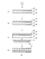
図9は、本発明の実施の形態5にかかる半導体素子の製造方法の製造プロセスの一部を示す図である。まず、n-FZウエハー21の表面側に、実施の形態1と同様にして、図30に示す構成と同様の表面側素子構造部22(詳細な構成については図示省略)を作製する(図9(a))。
【0063】
ついで、ウエハー21を裏返し、表面側素子構造部22の表面に、高剛性接着シート51を貼り付ける。高剛性接着シート51については、実施の形態3と同じであるので、重複する説明を省略する。さらに、高剛性接着シート51の表面に、パーティクル除去用接着シート52を貼り付ける(図9(b))。パーティクル除去用接着シート52としては、たとえばUV光の照射による硬化によって剥離可能なUV硬化型、加熱発泡により剥離可能な加熱発泡型、可視光の照射による硬化によって剥離可能な可視光硬化型、または機械的に剥離するタイプのフィルム状の接着シートを用いることができる。
【0064】
ついで、高剛性接着シート51およびパーティクル除去用接着シート52を貼り付けた状態で、ウエハー裏面をバックグラインドやエッチング等により研削し、表面側素子構造部22を含むウエハー全体の厚さを所望の厚さ、たとえば70μmとする(図9(c))。その後、パーティクル除去用接着シート52のタイプに合わせて、UV光の照射、または加熱発泡、または可視光の照射、または機械的に、パーティクル除去用接着シート52を剥離させ、パーティクル除去用接着シート52を取り除く。高剛性接着シート51は貼り付けられたままである(図9(d))。これ以降のプロセスは、実施の形態3の図6以降のプロセスと同じであるので、説明を省略する。
【0065】
上述した実施の形態5によれば、実施の形態3と同様に、ウエハー割れを防ぐことができる、ダイシングが容易である、設計通りのデバイス特性が得られる、オン電圧の低減を図ることができるという効果に加えて、ウエハー裏面の研削後にパーティクル除去用接着シート52を剥がしてからイオン注入をおこなうことにより、ウエハー裏面の研削時に発生した削り屑やその他の塵などのパーティクルを、イオン注入前に取り除くことができるので、パーティクルによる不良品の発生を防ぐことができるという効果が得られる。
【0066】
実施の形態6.
図10は、本発明の実施の形態6にかかる半導体素子の製造方法の製造プロセスの一部を示す図である。実施の形態6では、nドープのエピタキシャルウエハーを用いる。まず、n+半導体基板41上に成長したエピタキシャル層42の表面に、実施の形態1と同様にして、図30に示す構成と同様の表面側素子構造部22(詳細な構成については図示省略)を作製する(図10(a))。この表面側素子構造部22を作製する際の拡散工程においてn層が拡散していく。
【0067】
ついで、ウエハーを裏返し、表面側素子構造部22の表面に、高剛性接着シート51を貼り付け、さらに、高剛性接着シート51の表面に、パーティクル除去用接着シート52を貼り付ける(図10(b))。高剛性接着シート51およびパーティクル除去用接着シート52は、それぞれ実施の形態3および実施の形態5と同じであるので、重複する説明を省略する。ついで、その状態で、ウエハー裏面をバックグラインドやエッチング等により研削し、表面側素子構造部22を含むウエハー全体の厚さが所望の厚さ、たとえば70μmで、かつn+半導体基板41がたとえば10μmの厚さで残るようにする(図10(c))。
【0068】
その後、高剛性接着シート51からパーティクル除去用接着シート52を剥離させ、パーティクル除去用接着シート52を取り除く。高剛性接着シート51は貼り付けられたままである(図10(d))。これ以降のプロセスは、実施の形態4の図8以降のプロセスと同じであるので、説明を省略する。
【0069】
上述した実施の形態6によれば、実施の形態3と同様に、ウエハー割れを防ぐことができる、ダイシングが容易である、設計通りのデバイス特性が得られる、オン電圧の低減を図ることができるという効果に加えて、ウエハー裏面の研削後にパーティクル除去用接着シート52を剥がしてからイオン注入をおこなうことにより、ウエハー裏面の研削時に発生した削り屑やその他の塵などのパーティクルを、イオン注入前に取り除くことができるので、パーティクルによる不良品の発生を防ぐことができるという効果が得られる。
【0070】
実施の形態7.
図11は、本発明の実施の形態7にかかる半導体素子の製造方法のバックグラインド工程を詳細に説明するためのプロセス図である。まず、半導体ウエハー61の表面に、実施の形態1と同様にして、図30に示す構成と同様の表面側素子構造部(図示省略)を作製する。表面側素子構造部(図示省略)の作製後の表面には、パッシベーション膜を構成するポリイミド等による段差部62ができている(図11(a))。
【0071】
ついで、段差部62と段差部62の間の溝部分に充填剤63を充填して、溝部分を埋め、表面を平坦にする(図11(b))。充填剤63としては、たとえば加熱発泡により剥離可能な粘着剤を用いる。この粘着剤は、溝部分の幅が50〜100μm程度で、10μm程度の深さまでであれば、ドクターブレード法、スピンコート法またはスクリーン印刷法などにより充填可能である。
【0072】
ついで、充填剤63の充填により平坦化した表面に、一般的な厚さ(たとえば50μm程度)の保護テープ64を貼り付ける(図11(c))。テープ材質は、一般的に、EVA(エチレン−酢酸ビニルコポリマー)、PO(ポリオレフィン)系樹脂またはPETなどの樹脂基材である。そして、ウエハー61を、保護テープ64を下にして、バックグラインド装置の吸着台65に取り付け(図11(d))、バックグラインドをおこなう(図11(e))。バックグラインド終了後、吸着台65からウエハー61を取り外す(図11(f))。
【0073】
ついで、たとえば図示しないホットプレートの上に半導体ウエハー61を載せ、たとえば約150℃に加熱して、発泡剥離性の充填剤63を発泡させ、充填剤63と一緒に保護テープ64を剥がす(図11(g))。その後、必要に応じて、エッチングにより、ウエハー裏面側の表面処理をおこなう。そして、実施の形態1〜6のように、イオン注入やアニール、および裏面電極の形成などのウエハー裏面側の処理をおこない、ダイシングによってチップ状に切断する。
【0074】
上述した実施の形態7によれば、表面側素子構造部を形成した後、充填剤63によりその表面を平坦化してからバックグラインドをおこなうことによって、ウエハー61の裏面に段差部62のパターンを反映させることなく、裏面を平坦に研削することができる。また、ウエハー外周部が充填剤63により強化されるので、バックグラインド時に、ウエハー61の外周がバックグラインド装置の吸着台から浮き上がるのを防ぐことができる。したがって、ウエハー割れが起こるのを防ぐことができる。また、ウエハー61の裏面が局所的に削れてしまうのを防ぐことができるので、所望のデバイス特性が得られる。
【0075】
なお、充填剤63として、UV光の照射により硬化して剥離可能な粘着剤を用い、バックグラインド終了後にUV光を照射して、この粘着剤とともに保護テープ64を剥がすようにしてもよい。あるいは、充填剤63として、レジスト剤やポリイミドを用いてもよく、その場合には、保護テープ64を剥がした後に、レジストやポリイミドを、それらの剥離液を用いて除去すればよい。
【0076】
実施の形態8.
図12は、本発明の実施の形態8にかかる半導体素子の製造方法のバックグラインド工程を詳細に説明するためのプロセス図である。まず、半導体ウエハー61の表面に、実施の形態1と同様にして、図30に示す構成と同様の表面側素子構造部(図示省略)を作製する。表面側素子構造部(図示省略)の作製後の表面には、パッシベーション膜を構成するポリイミド等による段差部62ができている(図12(a))。
【0077】
ついで、段差部62の上から、一般的な厚さよりも厚い、EVA、PO、PETなどの樹脂でできた保護テープ66を貼り付ける(図12(b))。なお、EVA(エチレン−酢酸ビニルコポリマー)を基材としたバックグラインド用保護テープとしては、日東電工株式会社製の商品名BT−150E−ALやBT−150E−FLが使用できる。
【0078】
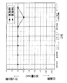
ここで、保護テープ66の厚さは、150〜200μmであるのが適当である。その理由は、本発明者らが、保護テープの厚さを30μm、50μm、100μm、150μm、175μm、200μm、250μm、300μmとして、ウエハー面内厚さの均一性を調べた結果、図13に示すように、テープの厚さが150〜200μmのときに、ウエハー面内厚さのばらつきが、デバイス性能を維持することが可能である3μm以下となるからである。
【0079】
保護テープが150μmよりも薄いと、ウエハー表面の段差部62によるパターンを十分に吸収することができないため、ウエハー面内厚さのばらつきが大きくなると考えられる。一方、保護テープが200μmよりも厚いと、テープ自体の厚さのばらつきや、テープが押されることによるばらつきなどの影響で、ウエハー面内厚さのばらつきが悪化すると考えられる。
【0080】
保護テープ66を貼り付けた後、ウエハー61を、保護テープ66を下にして、バックグラインド装置の吸着台65に取り付け(図12(c))、バックグラインドをおこなう(図12(d))。このとき、ウエハー裏面には、わずかに段差部62のパターンを反映した凹部67が形成されるが、図13から明らかなように、この凹部67の深さは3μm程度であり、その後のプロセスに及ぼす影響は極めて小さい。また、デバイス特性に及ぼす影響も極めて小さい。
【0081】
バックグラインド終了後、吸着台65からウエハー61を取り外し、保護テープ66を剥がす(図12(e))。その後、必要に応じて、エッチングにより、ウエハー裏面側の表面処理をおこなう。そして、実施の形態1〜6のように、イオン注入やアニール、および裏面電極の形成などのウエハー裏面側の処理をおこない、ダイシングによってチップ状に切断する。
【0082】
上述した実施の形態8によれば、表面側素子構造部を形成した後、厚い保護テープ66を貼り付けた状態でバックグラインドをおこなうことによって、ウエハー61の裏面に段差部62のパターンを極力反映させることなく、裏面をほぼ平坦に研削することができる。したがって、ウエハー割れが起こるのを防ぐことができる。また、ウエハー61の裏面が局所的に深く削れてしまうのを防ぐことができるので、所望のデバイス特性が得られる。なお、保護テープ66として、テープ基材を柔らかくして厚くしたときに面内圧さの均一性が良好なテープを用いても、同様の効果が得られる。
【0083】
実施の形態9.
図14は、本発明の実施の形態9にかかる半導体素子の製造方法のバックグラインド工程を詳細に説明するためのプロセス図である。まず、実施の形態7と同様にして、半導体ウエハー61の表面に、表面側素子構造部(図示省略)を作製し(図14(a))、パッシベーション膜を構成するポリイミド等による段差部62と段差部62との間の溝部分に、加熱発泡による剥離性を有する充填剤63を充填し、表面を平坦にする(図14(b))。充填剤63については、実施の形態7と同じであるので、重複する説明を省略する。
【0084】
ついで、充填剤63の充填により平坦化した表面に、両面接着タイプで、耐熱性UVテープ型の接着シート31を貼り付け(図14(c))、その接着シート31に支持基板32を貼り付ける(図14(d))。接着シート31および支持基板32については、実施の形態1と同じであるので、重複する説明を省略する。ついで、支持基板32の、素子と接合されていない側の面に、一般的な厚さ(たとえば100μm程度)の保護テープ64を貼り付け、それを、保護テープ64を下にして、バックグラインド装置の吸着台65に取り付け(図14(e))、バックグラインドをおこなう(図14(f))。バックグラインド終了後、吸着台65からウエハー61を取り外し、保護テープ64を剥がす(図14(g))。
【0085】
ついで、たとえば図示しないホットプレート等によりウエハー61をたとえば約150℃に加熱して、発泡剥離性の充填剤63を剥離させる(図14(h))。その後、必要に応じて、エッチングにより、ウエハー裏面側の表面処理をおこなう。そして、実施の形態1〜6のように、イオン注入やアニール、および裏面電極の形成などのウエハー裏面側の処理をおこない、UV光を照射して接着シート31および支持基板32を剥離させる(図14(h))。最後に、ダイシングによってチップ状に切断する(図14(i))。
【0086】
上述した実施の形態9によれば、表面側素子構造部を形成した後、充填剤63によりその表面を平坦化し、さらに支持基板32を接合した状態でバックグラインドをおこなうことによって、ウエハー61の裏面に段差部62のパターンを反映させることなく、裏面を平坦に研削することができる。また、ウエハー61が薄くなっても、支持基板32に接合されていることにより、バックグラインド後のプロセスでのウエハー61の反りを抑制することができる。したがって、ウエハー割れが起こるのを防ぐことができる。また、ウエハー61の裏面が局所的に削れてしまうのを防ぐことができるので、所望のデバイス特性が得られる。
【0087】
なお、充填剤63として、UV光の照射により硬化して剥離可能な粘着剤を用いてもよい。その場合には、ホットプレート等によるウエハー61の加熱は不要であり、バックグラインド後、充填剤63を充填した状態のまま裏面電極形成までのウエハー裏面処理をおこなう。そして、ダイシングの直前に、UV光を照射して接着シート31および支持基板32の剥離と同時に、充填剤63を除去する。
【0088】
【実施例】
実施例1.
上述した実施の形態1にしたがい、FS型IGBTを作製した。使用したn-FZウエハー21の直径は6インチであり、厚さは625μmであった。支持基板32として、石英ガラスウエハーを用いた。接着シート31として、UVテープ型シートを用いた。バックグラインド後のウエハー21の厚さは、ウエハー厚に対するウエハーの反り量や割れ率の関係を調べるため、70μm、80μm、90μmまたは100μmとした。
【0089】
また、バッファ層となるn+層23を形成するために、リンをイオン注入する際のドーズ量を5×1012cm-2とし、加速電圧を600keVとした。コレクタ層となるp+層24を形成するために、ボロンをイオン注入する際のドーズ量を1×1015cm-2とし、加速電圧を50keVとした。レーザーアニールでは、YAGの第3高調波(YAG3ω)パルスレーザーを、50%オーバーラップさせながら照射した。コレクタ電極となる裏面電極25は、アルミニウム、チタン、ニッケルおよび金からなり、合計で2μmの厚さとした。
【0090】
実施例2.
上述した実施の形態2にしたがい、FS型IGBTを作製した。使用したエピタキシャルウエハーの直径は6インチであった。バックグラインド後のウエハーの厚さは、70μm(n+半導体基板41の残りの厚さ:10μm)、80μm(n+半導体基板41の残りの厚さ:20μm)、90μm(n+半導体基板41の残りの厚さ:30μm)または100μm(n+半導体基板41の残りの厚さ:40μm)とした。レーザーアニールでは、XeClパルスレーザーを、90%オーバーラップさせながら照射した。支持基板32、接着シート31、ボロンのイオン注入および裏面電極25については、実施例1と同じであった。ただし、ウエハー裏面に対するリンのイオン注入はおこなわなかった。
【0091】
実施例3.
上述した実施の形態3にしたがい、FS型IGBTを作製した。支持基板32および接着シート31を用いずに、高剛性接着シート51を貼り付けた点を除いて、実施例1と同じであった。
【0092】
実施例4.
上述した実施の形態4にしたがい、FS型IGBTを作製した。支持基板32および接着シート31を用いずに、高剛性接着シート51を貼り付けた点を除いて、実施例2と同じであった。
【0093】
実施例5.
上述した実施の形態5にしたがい、FS型IGBTを作製した。支持基板32および接着シート31を用いずに、高剛性接着シート51およびパーティクル除去用接着シート52を貼り付けた点を除いて、実施例1と同じであった。
【0094】
実施例6.
上述した実施の形態6にしたがい、FS型IGBTを作製した。支持基板32および接着シート31を用いずに、高剛性接着シート51およびパーティクル除去用接着シート52を貼り付けた点を除いて、実施例2と同じであった。
【0095】
実施例7.
上述した実施の形態7にしたがい、FS型IGBTを作製した。使用したウエハー61の直径は6インチであった。充填剤63として、加熱発泡により剥離可能な粘着剤を用いた。バックグラインド後のウエハー61の厚さは、70μm、80μm、90μmまたは100μmとした。裏面電極は、アルミニウム、チタン、ニッケルおよび金からなり、合計で2μmの厚さとした。
【0096】
実施例8.
上述した実施の形態8にしたがい、FS型IGBTを作製した。使用したウエハー61の直径は6インチであった。使用した保護テープ66は、厚さがおおよそ150μmの樹脂テープであった。バックグラインド後のウエハー61の厚さは、70μm、80μm、90μmまたは100μmとした。裏面電極は、アルミニウム、チタン、ニッケルおよび金からなり、合計で2μmの厚さとした。
【0097】
実施例9.
上述した実施の形態9にしたがい、FS型IGBTを作製した。充填剤63として、加熱発泡により剥離可能な粘着剤を用いた。その他は、実施例2と同じであった。
【0098】
従来例1.
従来のFZウエハーを用いたFS型IGBTの製造プロセス(図31参照)にしたがい、FS型IGBTを作製した。支持基板32および接着シート31を用いていないことと、レーザーアニールの代わりに電気炉アニール(400℃で1時間)をおこなったことを除いて、実施例1と同じであった。
【0099】
従来例2.
従来のエピタキシャルウエハーを用いたFS型IGBTの製造プロセス(図32参照)にしたがい、FS型IGBTを作製した。支持基板32および接着シート31を用いていないことと、レーザーアニールの代わりに電気炉アニール(400℃で1時間)をおこなったことを除いて、実施例2と同じであった。
【0100】
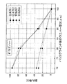
図15は、実施例1および実施例2について、裏面電極を形成した後(裏面蒸着後)のウエハーの反り量とバックグラインド後のウエハーの厚さとの関係を調べた結果を示す図である。ここで、反り量とは、ウエハーの中央と周縁との高さの差である。図15より、実施例1および実施例2のいずれも、バックグラインド後のウエハーの厚さを70μmまで薄くしても、裏面電極形成後のウエハーの反り量は、裏面電極形成後に割れが生じるときの反りの限界値である5.5mm(直径6インチのウエハーの場合)よりもはるかに小さいことがわかる。
【0101】
比較のため、従来例1および従来例2について、同様のことを調べた結果も併せて図15に示す。従来例1および従来例2では、バックグラインド後のウエハーの厚さを90μm以下にすると、裏面電極形成後のウエハーの反り量は、反りの限界値である5.5mm(直径6インチのウエハーの場合)を超えてしまう。具体的には、バックグラインド後のウエハーの厚さを70μmにしたときの裏面電極形成後のウエハーの反り量は、実施例1では2mmであり、実施例2では2.1mmであり、従来例1では11mmであり、従来例2では11.2mmである。
【0102】
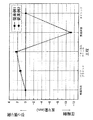
図16は、実施例1および実施例2において、バックグラインド後のウエハーの厚さが70μmであるものについて、工程ごとにウエハーの反り量を調べた結果を示す図である。なお、本明細書では、ウエハーの表面側が凹状になるときにウエハーに引っ張り応力が作用しており、凸状になるときに圧縮応力が作用しているとする。そして、ウエハーに引っ張り応力が作用している場合の反り量を正の値で表し、圧縮応力が作用している場合の反り量を負の値で表すことにする。図16より、実施例1および実施例2のいずれも、各工程においてほとんど反り量がないことがわかる。
【0103】
比較のため、図28に、従来例1および従来例2において、バックグラインド後のウエハーの厚さが70μmであるものについて、同様のことを調べた結果を示す。従来例1および従来例2では、裏面電極を形成する前は正の反り量が発生するが、裏面電極の形成により、おおよそ−11mmの反り量が発生している。
【0104】
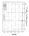
図17は、実施例1および実施例2について、素子の割れ率とバックグラインド後のウエハーの厚さとの関係を調べた結果を示す図である。比較のため、従来例1および従来例2について、同様のことを調べた結果も併せて図17に示す。図17に示すように、実施例1および実施例2のいずれも、バックグラインド後のウエハーの厚さを70μmまで薄くしても、割れ率は2%以下と極めて小さい。実施例1または実施例2において割れが発生するのは、UVテープ型の接着シートの剥離時と、ダイシング時であり、途中の工程ではほとんど割れない。それに対して、図17より、従来例1および従来例2では、バックグラインド後のウエハーの厚さが70μmであるものの割れ率は95%と極めて高い。
【0105】
図18は、実施例1および従来例1について、キャリア濃度分布を調べた結果を示す図である。図19は、実施例2および従来例2について、キャリア濃度分布を調べた結果を示す図である。ただし、いずれも、裏面電極をのぞいて、ウエハー裏面側からのSR(広がり抵抗法)により測定した。図18および図19より、実施例1および実施例2では、レーザーアニールを用いたことにより、ウエハー裏面のp層を従来例よりも高濃度化することができ、低オン電圧化が図れていることがわかる。
【0106】
図20は、実施例3〜実施例6について、裏面電極を形成した後のウエハーの反り量とバックグラインド後のウエハーの厚さとの関係を調べた結果を示す図である。比較のため、従来例1および従来例2の結果も併せて図20に示す。図20より、実施例3〜実施例6のいずれも、バックグラインド後のウエハーの厚さを70μmまで薄くしても、裏面電極形成後のウエハーの反り量は、裏面電極形成後に割れが生じるときの反りの限界値である5.5mm(直径6インチのウエハーの場合)よりも小さいことがわかる。具体的には、実施例3〜実施例6では、バックグラインド後のウエハーの厚さを70μmにしたときの裏面電極形成後のウエハーの反り量は、約3〜3.51mmである。
【0107】
図21は、実施例3および実施例4において、バックグラインド後のウエハーの厚さが70μmであるものについて、工程ごとにウエハーの反り量を調べた結果を示す図である。また、図22は、実施例5および実施例6において、バックグラインド後のウエハーの厚さが70μmであるものについて、工程ごとにウエハーの反り量を調べた結果を示す図である。図21および図22より、実施例3〜実施例6のいずれも、各工程においてほとんど反り量がないことがわかる。
【0108】
図23は、実施例3〜実施例6について、素子の割れ率とバックグラインド後のウエハーの厚さとの関係を調べた結果を示す図である。比較のため、従来例1および従来例2の結果も併せて図23に示す。図23に示すように、実施例3〜実施例6のいずれも、バックグラインド後のウエハーの厚さを70μmまで薄くしても、割れ率は5%以下と極めて小さい。実施例3〜実施例6において割れが発生するのは、高剛性接着シートやパーティクル除去用接着シートの剥離時と、ダイシング時であり、途中の工程ではほとんど割れない。
【0109】
実施例3および実施例5について、キャリア濃度分布を調べた結果を図18に、また実施例4および実施例6について、キャリア濃度分布を調べた結果を図19にそれぞれ示す。ただし、いずれも、裏面電極をのぞいて、ウエハー裏面側からのSRにより測定した。図18および図19より、実施例3〜実施例6では、レーザーアニールを用いたことにより、ウエハー裏面のp層を従来例よりも高濃度化することができ、低オン電圧化が図れていることがわかる。
【0110】
図24は、実施例7および実施例8について、裏面電極を形成した後のウエハーの反り量とバックグラインド後のウエハーの厚さとの関係を調べた結果を示す図である。比較のため、従来例1および従来例2の結果も併せて図24に示す。図24より、実施例7および実施例8のいずれも、バックグラインド後のウエハーの厚さを70μmまで薄くしても、裏面電極形成後のウエハーの反り量は、裏面電極形成後に割れが生じるときの反りの限界値である5.5mm(直径6インチのウエハーの場合)よりも小さいことがわかる。
【0111】
具体的には、実施例7および実施例8では、バックグラインド後のウエハーの厚さを70μmにしたときの裏面電極形成後のウエハーの反り量は、5.4mmである。つまり、ウエハー表面の凹凸形状のパターンをウエハー裏面に極力反映させずにバックグラインドをおこなうことによって、反り量が従来の半分程度に抑えられることがわかる。
【0112】
図25は、実施例7および実施例8について、素子の割れ率とバックグラインド後のウエハーの厚さとの関係を調べた結果を示す図である。比較のため、従来例1および従来例2の結果も併せて図25に示す。図25に示すように、バックグラインド後のウエハーの厚さを70μmにした場合の割れ率は、実施例7では30%であり、実施例8では35%である。従来例に比べて割れ率が低減した理由は、反り量を低減させ、ウエハー表面の凹凸形状のパターンがウエハー裏面に反映されることが原因で割れるのをほとんど失くしたことである。
【0113】
図26は、実施例9について、裏面電極を形成した後(裏面蒸着後)のウエハーの反り量とバックグラインド後のウエハーの厚さとの関係を調べた結果を示す図である。比較のため、実施例2の結果も併せて図26に示す。図26より、実施例9では、裏面電極形成後のウエハーの反り量は、実施例2よりも小さいことがわかる。具体的には、実施例9では、バックグラインド後のウエハーの厚さを70μmにしたときの裏面電極形成後のウエハーの反り量は、1.8mmである。
【0114】
図27は、実施例9について、素子の割れ率とバックグラインド後のウエハーの厚さとの関係を調べた結果を示す図である。比較のため、実施例2の結果も併せて図27に示す。図27に示すように、実施例9では、バックグラインド後のウエハーの厚さを70μmにした場合、割れ率は実施例2よりも小さいことがわかる。
【0115】
以上において、本発明は、半導体素子の表面構成は問わないので、半導体素子の表面側素子構造部はプレーナ型でもトレンチ型でもよい。また、本発明は、バックグラインド後のウエハーの厚さが70μmであるIGBTに限らず、ウエハー裏面をバックグラインドしてウエハー厚さを100μm以下にする工程を有する電力用半導体素子の製造方法に適用できる。また、実施の形態9のように、実施の形態1〜実施の形態6のいずれかと、実施の形態7または実施の形態8とを組み合わせてもよい。
【0116】
【発明の効果】
本発明によれば、半導体ウエハーの表面側に、半導体素子の表面側素子構造部を形成した後、その表面に支持基板または高剛性接着シートを接合し、この状態でバックグラインドをおこなってウエハーを薄くした後、ウエハー裏面に対する処理をおこなうことにより、ウエハー裏面に対する処理をおこなっている間のウエハーの反りや、ウエハーに作用する応力を抑制することができるので、ウエハー裏面に対する処理をおこなっている間にウエハーが割れるのを防ぐことができる。また、応力の発生源となる電気炉アニールに代えて、レーザーアニールを採用することにより、ウエハーに作用する応力を抑制することができるので、ウエハーが割れるのを防ぐことができる。また、ウエハーの反りが小さくなるので、設計通りのデバイス特性が得られる。
【0117】
また、本発明によれば、半導体ウエハーの裏面に、高剛性接着シートおよびパーティクル除去用接着シートを貼り付けた状態でバックグラインドをおこない、裏面研削終了後にパーティクル除去用接着シートを剥がしてからイオン注入をおこなうことにより、ウエハー裏面の研削時に発生した削り屑やその他の塵などのパーティクルを、イオン注入前に取り除くことができるので、パーティクルによる不良品の発生を防ぐことができる。
【0118】
また、本発明によれば、表面側素子構造部を形成した後、充填剤によりその表面を平坦化してからバックグラインドをおこなうことにより、あるいは、表面側素子構造部上に厚い保護テープを貼り付けてバックグラインドをおこなうことにより、ウエハーの裏面に、ウエハー表面の段差部のパターンを反映させることなく、裏面を平坦に研削することができる。また、ウエハー外周部が充填剤により強化されるので、バックグラインド時に、ウエハーの外周がバックグラインド装置の吸着台から浮き上がるのを防ぐことができる。したがって、ウエハー割れが起こるのを防ぐことができる。また、ウエハーの裏面が局所的に削れてしまうのを防ぐことができるので、所望のデバイス特性が得られる。
【図面の簡単な説明】
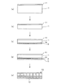
【図1】本発明の実施の形態1にかかる半導体素子の製造方法の製造プロセスの一部を示す図である。
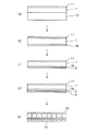
【図2】図1に示す製造プロセスの続きを示す図である。
【図3】本発明の実施の形態2にかかる半導体素子の製造方法の製造プロセスの一部を示す図である。
【図4】図3に示す製造プロセスの続きを示す図である。
【図5】本発明の実施の形態3にかかる半導体素子の製造方法の製造プロセスの一部を示す図である。
【図6】図5に示す製造プロセスの続きを示す図である。
【図7】本発明の実施の形態4にかかる半導体素子の製造方法の製造プロセスの一部を示す図である。
【図8】図7に示す製造プロセスの続きを示す図である。
【図9】本発明の実施の形態5にかかる半導体素子の製造方法の製造プロセスの一部を示す図である。
【図10】本発明の実施の形態6にかかる半導体素子の製造方法の製造プロセスの一部を示す図である。
【図11】本発明の実施の形態7にかかる半導体素子の製造方法のバックグラインド工程を詳細に説明するためのプロセス図である。
【図12】本発明の実施の形態8にかかる半導体素子の製造方法のバックグラインド工程を詳細に説明するためのプロセス図である。
【図13】実施の形態8において、保護テープの厚さを変えてウエハー面内厚さの均一性を調べた結果を示す特性図である。
【図14】本発明の実施の形態9にかかる半導体素子の製造方法のバックグラインド工程を詳細に説明するためのプロセス図である。
【図15】実施例1、実施例2、従来例1および従来例2について、裏面電極を形成した後のウエハーの反り量とバックグラインド後のウエハーの厚さとの関係を調べた結果を示す図である。
【図16】実施例1および実施例2について、工程ごとにウエハーの反り量を調べた結果を示す図である。
【図17】実施例1、実施例2、従来例1および従来例2について、素子の割れ率とバックグラインド後のウエハーの厚さとの関係を調べた結果を示す図である。
【図18】実施例1、実施例3、実施例5および従来例1について、キャリア濃度分布を調べた結果を示す図である。
【図19】実施例2、実施例4、実施例6および従来例2について、キャリア濃度分布を調べた結果を示す図である。
【図20】実施例3、実施例4、実施例5および実施例6について、裏面電極を形成した後のウエハーの反り量とバックグラインド後のウエハーの厚さとの関係を調べた結果を示す図である。
【図21】実施例3および実施例4において、工程ごとにウエハーの反り量を調べた結果を示す図である。
【図22】実施例5および実施例6において、工程ごとにウエハーの反り量を調べた結果を示す図である。
【図23】実施例3、実施例4、実施例5および実施例6について、素子の割れ率とバックグラインド後のウエハーの厚さとの関係を調べた結果を示す図である。
【図24】実施例7および実施例8について、裏面電極を形成した後のウエハーの反り量とバックグラインド後のウエハーの厚さとの関係を調べた結果を示す図である。
【図25】実施例7および実施例8について、素子の割れ率とバックグラインド後のウエハーの厚さとの関係を調べた結果を示す図である。
【図26】実施例9および実施例2について、裏面電極を形成した後のウエハーの反り量とバックグラインド後のウエハーの厚さとの関係を調べた結果を示す図である。
【図27】実施例9および実施例2について、素子の割れ率とバックグラインド後のウエハーの厚さとの関係を調べた結果を示す図である。
【図28】従来例1および従来例2について、工程ごとにウエハーの反り量を調べた結果を示す図である。
【図29】NPT型IGBTの構成を示す断面図である。
【図30】FS型IGBTの構成を示す断面図である。
【図31】従来のFZウエハーを用いたFS型IGBTの製造プロセスを示す図である。
【図32】従来のエピタキシャルウエハーを用いたFS型IGBTの製造プロセスを示す図である。
【図33】従来のバックグラインド工程を詳細に説明するためのプロセス図である。
【符号の説明】
21,61 半導体ウエハー
22 表面側素子構造部
27 チップ
31 両面接着タイプの接着シート
32 支持基板
41 n+半導体基板
42 エピタキシャル層
51 高剛性接着シート
52 パーティクル除去用接着シート
63 充填剤
66 保護テープ[0001]
BACKGROUND OF THE INVENTION
The present invention relates to a method for manufacturing a semiconductor device, and more particularly to a method for manufacturing a power semiconductor device such as an insulated gate bipolar transistor (hereinafter referred to as IGBT).
[0002]
[Prior art]
The IGBT is a voltage-driven type element that has a low on-voltage and high-speed switching characteristics, and its application range has expanded from an industrial field such as an inverter to a field of consumer equipment such as a microwave oven. Conventionally, IGBTs have a punch-through (hereinafter referred to as PT) type, non-punch-through (hereinafter referred to as NPT) type, and field stop (hereinafter referred to as FS) type, and an n-channel vertical type. A double diffusion structure is the mainstream.
[0003]
PT type IGBT is p + N on the semiconductor substrate + Buffer layer and n - The active layer is formed using an epitaxial wafer obtained by epitaxial growth. Therefore, for example, in a device with a withstand voltage of 600 V, the thickness of the active layer is about 70 μm, but the total thickness including the substrate is about 200 to 300 μm.
[0004]
FIG. 29 shows a shallow p with a low dose. + It is sectional drawing which shows the structure for 1/2 cell of NPT type IGBT which has a collector layer. As shown in FIG. 29, for example, n made of an FZ wafer - The semiconductor substrate is an
[0005]
The
[0006]
FIG. 30 is a cross-sectional view showing the configuration of 1/2 cell of FS type IGBT. As shown in FIG. 30, the element structure on the substrate surface side is the same as the NPT type element shown in FIG. On the back side of the substrate, n -
[0007]
Recently, in order to further reduce the total loss, an attempt has been made to thin the wafer and reduce the device thickness as much as possible. For example, in the case of an element having a withstand voltage of 600 V, the thickness of the FS-IGBT is assumed to be about 70 μm. When the breakdown voltage class is lowered, the thickness of the element is further reduced. As described below, a method for polishing an FZ wafer and a method for polishing an epitaxial wafer are known as methods for manufacturing such a thickness FS type IGBT or a device similar thereto.
[0008]
FIG. 31 is a diagram showing a manufacturing process of an FS type IGBT using a conventional FZ wafer. As shown in FIG. 31, first, n which becomes the
[0009]
Next, for example, phosphorus (P), which is an n-type impurity, and boron (B), which is a p-type impurity, are ion-implanted from the back surface of the wafer, and a heat treatment (annealing) is performed at 350 to 500 ° C. in an electric furnace. 10 and the
[0010]
FIG. 32 is a diagram showing a manufacturing process of an FS type IGBT using a conventional epitaxial wafer. As shown in FIG. 32, first, n which becomes the
[0011]
Next, boron, which is a p-type impurity, is ion-implanted from the back surface of the wafer, and annealed at 350 to 500 ° C. in an electric furnace to form the collector layer 8 (FIG. 32C). Next, a
[0012]
FIG. 33 is a process diagram for explaining the conventional back grinding process in detail. As shown in FIG. 33, in the back grinding process, first, a
[0013]
Then, back grind. At this time, since the
[0014]
[Problems to be solved by the invention]
However, if an element having a thickness of, for example, about 70 μm is manufactured by the above-described conventional manufacturing method, the wafer after back grinding is too thin, and therefore, when performing ion implantation from the back side of the wafer, the wafer is likely to be broken. is there. Further, when a metal film serving as a collector electrode is deposited on the back surface of the wafer, the metal film becomes a film having a large compressive stress when viewed from the substrate side, and thus there is a problem that the wafer is likely to be cracked.
[0015]
In addition, there is a problem that the wafer is easily broken by the stress generated in the wafer during annealing in the electric furnace. Further, even if the wafer is not cracked, the wafer is greatly warped by the compressive stress, so that there is a problem that dicing becomes difficult. In addition, since the shape of the chip after dicing is distorted, the designed characteristics may not be obtained.
[0016]
Further, in the above-described conventional back grinding process, the back surface of the wafer becomes concave and convex due to the back grinding, and the wafer is cracked deeply particularly in a portion where vacuum suction is strong (see FIG. 33 (e), central recess). There is a problem that it is likely to occur. In addition, since the strength of the outer peripheral portion of the wafer is low, there is a problem that the outer periphery of the wafer is lifted from the suction table of the back grinding apparatus and causes a wafer crack. Moreover, there is a possibility that desired device characteristics cannot be obtained because the back surface of the wafer is locally scraped.
[0017]
The present invention has been made in view of the above problems, and suppresses warping of the wafer and stress acting on the wafer when manufacturing a semiconductor device such as an IGBT having a thin device thickness by back grinding the back surface of the wafer. Accordingly, it is an object of the present invention to provide a method for manufacturing a semiconductor element that can manufacture a semiconductor element while preventing the wafer from being broken.
[0018]
Another object of the present invention is to provide a method of manufacturing a semiconductor device that prevents the wafer from cracking by preventing local chipping on the back surface of the wafer during back grinding.
[0019]
[Means for Solving the Problems]
In order to achieve the above object, a method for manufacturing a semiconductor device according to the present invention includes a step of manufacturing a surface element structure portion of a semiconductor element on a surface of a semiconductor wafer, and a step of manufacturing the surface element structure portion of the semiconductor wafer. Side surface High Rigid adhesive sheet Paste Process, A step of further bonding an adhesive sheet for particle removal to the high-rigidity adhesive sheet; Above High rigidity Adhesive sheet And the particle removing adhesive sheet The Pasted Grinding the back surface of the semiconductor wafer in a state so that the surface on the back surface side of the semiconductor wafer is flat; The step of peeling the adhesive sheet for particle removal, and after peeling the adhesive sheet for particle removal, Ion implantation, the implanted impurity is activated by laser annealing, and a back surface structure is fabricated so that no stress is generated on the ground surface of the semiconductor wafer, and the back surface structure is fabricated. From the semiconductor wafer High rigidity A step of peeling the adhesive sheet; High rigidity Adhesive sheet After peeling And a step of cutting the semiconductor wafer into chips.
[0020]
In the present invention, when the back surface structure is manufactured, ion implantation may be performed, and the implanted impurities may be activated by a laser annealing method.
[0023]
In this invention, after affixing the adhesive sheet to the semiconductor wafer, further affixing an adhesive sheet for particle removal to the adhesive sheet, and after grinding the back surface of the wafer, after peeling off the adhesive sheet for particle removal, It is good also as a structure which produces a back surface structure.
[0024]
According to the present invention, after the surface element structure portion of the semiconductor element is formed on the surface side of the semiconductor wafer, the high-rigidity adhesive sheet is pasted on the surface, and in this state, the back grinding is performed to thin the wafer. By performing the processing on the wafer back surface, the warp of the wafer and the stress acting on the wafer during the processing on the wafer back surface are suppressed.
[0025]
In addition, according to the present invention, the backside grinding is performed with the high-rigidity adhesive sheet and the particle removal adhesive sheet attached to the back surface of the semiconductor wafer, and after the backside grinding is finished, the particle removal adhesive sheet is peeled off before the back surface structure. Thus, particles such as shavings and other dust generated during grinding of the back surface of the wafer are removed before the back surface structure is manufactured.
[0030]
DETAILED DESCRIPTION OF THE INVENTION
Hereinafter, embodiments of the present invention will be described in detail with reference to the drawings. In the embodiment, a case where an IGBT is manufactured by the method of the present invention will be described as an example. In the following description of each embodiment and the accompanying drawings, the same reference numerals are assigned to the same components.
[0031]
1 and 2 are diagrams showing a manufacturing process of the method for manufacturing a semiconductor device according to the first embodiment of the present invention. First, n - On the surface side of the
[0032]
Then, a surface electrode made of an Al—Si film, that is, an emitter electrode is formed, and heat treatment is performed at about 400 to 500 ° C. to make the Al—Si film a low resistance wiring having stable bonding. A polyimide passivation film is laminated on the entire surface, and a surface-side
[0033]
Next, the
[0034]
Next, with the
[0035]
After that, annealing is performed by irradiating the back surface of the wafer with a laser to form a buffer layer. + P to be
[0036]
Next, a plurality of metals such as aluminum, titanium, nickel, and gold are vapor-deposited on the back surface of the wafer to form a
[0037]
Next, a
[0038]
According to the first embodiment described above, after the front surface side
[0039]
In the first embodiment described above, when a heat-foamed tape-type sheet is used as the
[0040]
In the case of manufacturing an NPT type IGBT, in
[0041]
3 and 4 are diagrams showing a manufacturing process of the semiconductor element manufacturing method according to the second embodiment of the present invention. In the second embodiment, an n-doped epitaxial wafer is used. First, n + On the surface side of the epitaxial wafer on which the
[0042]
Next, the wafer is turned over, and the
[0043]
Next, with the
[0044]
After that, annealing is performed by irradiating the back surface of the wafer with a laser to form a collector layer. + The
[0045]
Next, for the same reason as in the first embodiment, a
[0046]
According to the second embodiment described above, similar to the first embodiment, it is possible to suppress the warpage of the wafer and the stress acting on the wafer during the processing on the wafer back surface, and also the laser annealing. By adopting, the stress acting on the wafer can be suppressed, so that the wafer can be prevented from cracking during the processing on the wafer back surface. Further, dicing is easy and device characteristics as designed can be obtained. Also, p by laser annealing + The on-voltage can be reduced by increasing the concentration of the
[0047]
5 and 6 are diagrams showing a manufacturing process of the method for manufacturing a semiconductor device according to the third embodiment of the present invention. First, n - On the surface side of the
[0048]
Next, the
[0049]
Further, as the adhesive of the high-rigidity
[0050]
Next, with the high-rigidity
[0051]
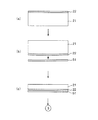
After that, annealing is performed by irradiating the back surface of the wafer with a laser to form a buffer layer. + P to be
[0052]
Next, a
[0053]
Next, a
[0054]
If the high-rigidity
[0055]
According to the third embodiment described above, after forming the surface-
[0056]
Note that in the case where an NPT type IGBT is manufactured, in
[0057]
7 and 8 are diagrams showing a manufacturing process of the method for manufacturing a semiconductor device according to the fourth embodiment of the present invention. In the fourth embodiment, an n-doped epitaxial wafer is used. First, n + On the surface of the
[0058]
Next, the wafer is turned over, and a high-rigidity
[0059]
After that, annealing is performed by irradiating the back surface of the wafer with a laser to form a collector layer. + The
[0060]
Next, a
[0061]
According to the above-described fourth embodiment, similarly to the third embodiment, it is possible to suppress the warpage of the wafer during the processing on the wafer back surface and the stress acting on the wafer. By adopting, the stress acting on the wafer can be suppressed, so that the wafer can be prevented from cracking during the processing on the wafer back surface. Further, dicing is easy and device characteristics as designed can be obtained. Also, p by laser annealing + The on-voltage can be reduced by increasing the concentration of the
[0062]
FIG. 9 is a diagram showing a part of a manufacturing process of the method for manufacturing a semiconductor device according to the fifth embodiment of the present invention. First, n - On the surface side of the
[0063]
Next, the
[0064]
Next, with the high-rigidity
[0065]
According to the above-described fifth embodiment, similarly to the third embodiment, wafer cracking can be prevented, dicing is easy, device characteristics as designed can be obtained, and ON voltage can be reduced. In addition to the above effects, by removing the particle removal
[0066]
FIG. 10 is a diagram showing a part of the manufacturing process of the method for manufacturing a semiconductor device according to the sixth embodiment of the present invention. In the sixth embodiment, an n-doped epitaxial wafer is used. First, n + On the surface of the
[0067]
Next, the wafer is turned over, and a high-rigidity
[0068]
Thereafter, the particle removing
[0069]
According to the above-described sixth embodiment, as in the third embodiment, wafer cracking can be prevented, dicing is easy, device characteristics as designed can be obtained, and ON voltage can be reduced. In addition to the above effects, by removing the particle removal
[0070]
FIG. 11 is a process diagram for explaining in detail the back grinding process of the semiconductor device manufacturing method according to the seventh exemplary embodiment of the present invention. First, on the surface of the
[0071]
Next, a
[0072]
Next, a
[0073]
Next, for example, the
[0074]
According to the above-described seventh embodiment, after the surface-side element structure portion is formed, the surface of the
[0075]
Note that an adhesive that can be cured and peeled off by irradiation with UV light may be used as the
[0076]
FIG. 12 is a process diagram for explaining in detail the back grinding process of the semiconductor device manufacturing method according to the eighth exemplary embodiment of the present invention. First, on the surface of the
[0077]
Next, a
[0078]
Here, it is appropriate that the thickness of the
[0079]
If the protective tape is thinner than 150 μm, the pattern due to the stepped
[0080]
After affixing the
[0081]
After the back grinding, the
[0082]
According to the above-described eighth embodiment, the pattern of the stepped
[0083]
FIG. 14 is a process diagram for explaining in detail the back grinding process of the semiconductor device manufacturing method according to the ninth exemplary embodiment of the present invention. First, in the same manner as in the seventh embodiment, a surface-side element structure portion (not shown) is formed on the surface of the semiconductor wafer 61 (FIG. 14A), and a
[0084]
Next, a double-sided adhesive heat-resistant UV tape-
[0085]
Next, the
[0086]
According to the above-described ninth embodiment, after the surface-side element structure portion is formed, the surface is flattened by the
[0087]
As the
[0088]
【Example】
Example 1.
In accordance with the first embodiment described above, an FS type IGBT was manufactured. N used - The diameter of the
[0089]
N serving as a buffer layer + In order to form the
[0090]
Example 2
In accordance with the second embodiment described above, an FS type IGBT was manufactured. The diameter of the epitaxial wafer used was 6 inches. The thickness of the wafer after back grinding is 70 μm (n + The remaining thickness of the semiconductor substrate 41: 10 μm), 80 μm (n + The remaining thickness of the semiconductor substrate 41: 20 μm), 90 μm (n + The remaining thickness of the semiconductor substrate 41: 30 μm) or 100 μm (n + The remaining thickness of the
[0091]
Example 3
In accordance with the third embodiment described above, an FS type IGBT was manufactured. The same as Example 1 except that the high-rigidity
[0092]
Example 4
In accordance with the fourth embodiment described above, an FS type IGBT was manufactured. It was the same as Example 2 except that the high-rigidity
[0093]
According to the fifth embodiment described above, an FS type IGBT was manufactured. It was the same as Example 1 except that the high-rigidity
[0094]
Example 6
In accordance with the above-described sixth embodiment, an FS type IGBT was manufactured. Example 2 was the same as Example 2 except that the high-rigidity
[0095]
Example 7
In accordance with the seventh embodiment described above, an FS type IGBT was manufactured. The
[0096]
Example 8 FIG.
In accordance with the above-described eighth embodiment, an FS type IGBT was manufactured. The diameter of the
[0097]
Example 9
In accordance with the ninth embodiment described above, an FS type IGBT was manufactured. As the
[0098]
Conventional Example 1
The FS type IGBT was manufactured according to the manufacturing process (see FIG. 31) of the FS type IGBT using the conventional FZ wafer. Example 1 was the same as Example 1 except that the
[0099]
Conventional Example 2
The FS type IGBT was manufactured according to the manufacturing process of the FS type IGBT using the conventional epitaxial wafer (see FIG. 32). Example 2 was the same as Example 2 except that the
[0100]
FIG. 15 is a diagram showing the results of examining the relationship between the amount of warpage of the wafer after forming the back electrode (after back surface deposition) and the thickness of the wafer after back grinding for Example 1 and Example 2. Here, the amount of warpage is the difference in height between the center and the periphery of the wafer. From FIG. 15, in both Example 1 and Example 2, even when the thickness of the wafer after back grinding is reduced to 70 μm, the amount of warpage of the wafer after forming the back electrode is such that cracking occurs after the back electrode is formed. It can be seen that it is much smaller than 5.5 mm (in the case of a wafer having a diameter of 6 inches) which is the limit value of the warpage of the wafer.
[0101]
For comparison, FIG. 15 also shows the results of examining the same for Conventional Example 1 and Conventional Example 2. In Conventional Example 1 and Conventional Example 2, when the thickness of the wafer after back grinding is set to 90 μm or less, the warpage amount of the wafer after forming the back electrode is 5.5 mm (a 6-inch diameter wafer). Case). Specifically, when the thickness of the wafer after back grinding is 70 μm, the amount of warpage of the wafer after forming the back electrode is 2 mm in Example 1, 2.1 mm in Example 2, and the conventional example 1 is 11 mm, and the conventional example 2 is 11.2 mm.
[0102]
FIG. 16 is a diagram showing the results of examining the amount of warpage of a wafer for each step in Example 1 and Example 2 where the thickness of the wafer after back grinding is 70 μm. In this specification, it is assumed that a tensile stress acts on the wafer when the surface side of the wafer becomes concave, and a compressive stress acts when the wafer becomes convex. The warpage amount when a tensile stress is acting on the wafer is expressed as a positive value, and the warpage amount when a compressive stress is acting is expressed as a negative value. From FIG. 16, it can be seen that both Example 1 and Example 2 have almost no warpage in each step.
[0103]
For comparison, FIG. 28 shows the result of examining the same in the conventional example 1 and the conventional example 2 in which the wafer thickness after back grinding is 70 μm. In Conventional Example 1 and Conventional Example 2, a positive warp amount occurs before the back electrode is formed, but a warp amount of approximately -11 mm occurs due to the formation of the back electrode.
[0104]
FIG. 17 is a diagram showing the results of examining the relationship between the element cracking rate and the thickness of the wafer after back grinding for Example 1 and Example 2. For comparison, FIG. 17 also shows the results of examining the same for Conventional Example 1 and Conventional Example 2. As shown in FIG. 17, in both Example 1 and Example 2, even when the thickness of the wafer after back grinding is reduced to 70 μm, the cracking ratio is as small as 2% or less. In Example 1 or Example 2, cracking occurs when the UV tape-type adhesive sheet is peeled off and during dicing, and is hardly cracked in the middle of the process. On the other hand, as shown in FIG. 17, in the conventional example 1 and the conventional example 2, although the wafer thickness after the back grinding is 70 μm, the cracking rate is as high as 95%.
[0105]
FIG. 18 is a diagram showing the results of examining the carrier concentration distribution in Example 1 and Conventional Example 1. FIG. 19 is a diagram showing the results of examining the carrier concentration distribution in Example 2 and Conventional Example 2. However, in all cases, measurement was performed by SR (spreading resistance method) from the back side of the wafer except for the back surface electrode. As shown in FIGS. 18 and 19, in Example 1 and Example 2, by using laser annealing, the p layer on the back surface of the wafer can be made higher in concentration than in the conventional example, and a low on-voltage can be achieved. I understand that.
[0106]
FIG. 20 is a diagram showing the results of examining the relationship between the amount of warpage of the wafer after forming the back electrode and the thickness of the wafer after back grinding for Example 3 to Example 6. For comparison, the results of Conventional Example 1 and Conventional Example 2 are also shown in FIG. From FIG. 20, in all of Examples 3 to 6, even when the thickness of the wafer after back grinding is reduced to 70 μm, the amount of warpage of the wafer after forming the back electrode is such that cracking occurs after the back electrode is formed. It can be seen that it is smaller than 5.5 mm (in the case of a wafer having a diameter of 6 inches) which is the limit value of the warpage of the wafer. Specifically, in Examples 3 to 6, the amount of warpage of the wafer after forming the back electrode when the thickness of the wafer after back grinding is 70 μm is about 3 to 3.51 mm.
[0107]
FIG. 21 is a diagram showing the results of examining the amount of warpage of a wafer for each step in Example 3 and Example 4 where the wafer thickness after back grinding is 70 μm. FIG. 22 is a diagram showing the results of examining the amount of warpage of the wafer for each step in Example 5 and Example 6 where the thickness of the wafer after back grinding is 70 μm. From FIG. 21 and FIG. 22, it can be seen that all of Examples 3 to 6 have almost no warpage in each step.
[0108]
FIG. 23 is a diagram showing the results of examining the relationship between the element cracking rate and the thickness of the wafer after back grinding for Examples 3 to 6. For comparison, the results of Conventional Example 1 and Conventional Example 2 are also shown in FIG. As shown in FIG. 23, in all of Examples 3 to 6, even when the thickness of the wafer after back grinding is reduced to 70 μm, the cracking rate is as small as 5% or less. In Examples 3 to 6, cracks occur when the high-rigidity adhesive sheet or the particle removal adhesive sheet is peeled off and during dicing, and are hardly cracked in the middle of the process.
[0109]
FIG. 18 shows the result of examining the carrier concentration distribution for Example 3 and Example 5, and FIG. 19 shows the result of examining the carrier concentration distribution for Example 4 and Example 6, respectively. However, all measured by SR from the wafer back surface side except for the back electrode. As shown in FIGS. 18 and 19, in Examples 3 to 6, the laser annealing can be used to increase the concentration of the p-layer on the back surface of the wafer as compared to the conventional example, thereby reducing the on-voltage. I understand that.
[0110]
FIG. 24 is a diagram showing the results of examining the relationship between the amount of warpage of the wafer after forming the back electrode and the thickness of the wafer after back grinding for Example 7 and Example 8. For comparison, the results of Conventional Example 1 and Conventional Example 2 are also shown in FIG. 24, in both Example 7 and Example 8, even when the thickness of the wafer after back grinding is reduced to 70 μm, the amount of warpage of the wafer after forming the back electrode is such that cracking occurs after the back electrode is formed. It can be seen that it is smaller than 5.5 mm (in the case of a wafer having a diameter of 6 inches) which is the limit value of the warpage of the wafer.
[0111]
Specifically, in Example 7 and Example 8, when the thickness of the wafer after back grinding is 70 μm, the amount of warpage of the wafer after forming the back electrode is 5.4 mm. That is, it can be seen that the amount of warpage can be reduced to about half of the conventional amount by performing back grinding without reflecting the uneven pattern on the wafer surface to the back surface of the wafer as much as possible.
[0112]
FIG. 25 is a diagram showing the results of examining the relationship between the element cracking rate and the thickness of the wafer after back grinding for Example 7 and Example 8. For comparison, the results of Conventional Example 1 and Conventional Example 2 are also shown in FIG. As shown in FIG. 25, the cracking rate when the thickness of the wafer after back grinding is 70 μm is 30% in Example 7 and 35% in Example 8. The reason why the cracking ratio is reduced compared to the conventional example is that the amount of warpage is reduced, and the cracks due to the fact that the uneven pattern on the wafer surface is reflected on the back surface of the wafer are almost lost.
[0113]
FIG. 26 is a diagram showing the results of examining the relationship between the amount of warpage of the wafer after forming the back surface electrode (after back surface deposition) and the thickness of the wafer after back grinding in Example 9. For comparison, the results of Example 2 are also shown in FIG. FIG. 26 shows that in Example 9, the amount of warpage of the wafer after forming the back electrode is smaller than that in Example 2. Specifically, in Example 9, the amount of warpage of the wafer after forming the back electrode when the thickness of the wafer after back grinding is 70 μm is 1.8 mm.
[0114]
FIG. 27 is a diagram showing the results of examining the relationship between the element cracking rate and the thickness of the wafer after back grinding in Example 9. For comparison, the results of Example 2 are also shown in FIG. As shown in FIG. 27, in Example 9, it can be seen that the crack rate is smaller than that in Example 2 when the thickness of the wafer after back grinding is set to 70 μm.
[0115]
In the above, since the surface configuration of the semiconductor element is not limited in the present invention, the surface side element structure portion of the semiconductor element may be a planar type or a trench type. Further, the present invention is not limited to an IGBT in which the thickness of a wafer after back grinding is 70 μm, but is applied to a method for manufacturing a power semiconductor device including a step of back grinding the back surface of the wafer to reduce the wafer thickness to 100 μm or less. it can. Further, as in the ninth embodiment, any one of the first to sixth embodiments may be combined with the seventh or eighth embodiment.
[0116]
【The invention's effect】
According to the present invention, after the surface element structure portion of the semiconductor element is formed on the surface side of the semiconductor wafer, the support substrate or the high-rigidity adhesive sheet is bonded to the surface, and in this state, the back grinding is performed and the wafer is bonded. After thinning, processing on the back side of the wafer can suppress warping of the wafer while processing the back side of the wafer and stress acting on the wafer, so that processing on the back side of the wafer is performed. It is possible to prevent the wafer from cracking. In addition, by adopting laser annealing instead of electric furnace annealing, which is a source of stress generation, stress acting on the wafer can be suppressed, so that the wafer can be prevented from cracking. Further, since the warpage of the wafer is reduced, device characteristics as designed can be obtained.
[0117]
Further, according to the present invention, the back grinding is performed with the high-rigidity adhesive sheet and the particle removal adhesive sheet attached to the back surface of the semiconductor wafer, and after the back surface grinding is finished, the particle removal adhesive sheet is peeled off and then ion implantation is performed. By carrying out the process, particles such as shavings and other dust generated during grinding of the back surface of the wafer can be removed before ion implantation, thereby preventing generation of defective products due to the particles.
[0118]
Further, according to the present invention, after the surface side element structure is formed, the surface is planarized with a filler and then back-grinded, or a thick protective tape is applied on the surface side element structure. By performing back grinding, the back surface can be ground flat without reflecting the pattern of the stepped portion on the wafer surface on the back surface of the wafer. Further, since the outer peripheral portion of the wafer is reinforced by the filler, it is possible to prevent the outer periphery of the wafer from being lifted from the adsorption table of the back grinding apparatus during back grinding. Therefore, it is possible to prevent the wafer from cracking. In addition, since the back surface of the wafer can be prevented from being locally scraped, desired device characteristics can be obtained.
[Brief description of the drawings]
FIG. 1 is a diagram showing a part of a manufacturing process of a semiconductor device manufacturing method according to a first embodiment of the present invention;
FIG. 2 is a diagram showing a continuation of the manufacturing process shown in FIG. 1;
FIG. 3 is a diagram showing a part of the manufacturing process of the semiconductor device manufacturing method according to the second exemplary embodiment of the present invention;
FIG. 4 is a diagram showing a continuation of the manufacturing process shown in FIG. 3;
FIG. 5 is a diagram showing a part of the manufacturing process of the semiconductor device manufacturing method according to the third exemplary embodiment of the present invention;
6 is a diagram showing a continuation of the manufacturing process shown in FIG. 5. FIG.
FIG. 7 is a diagram showing a part of the manufacturing process of the semiconductor element manufacturing method according to the fourth exemplary embodiment of the present invention;
8 is a diagram showing a continuation of the manufacturing process shown in FIG. 7. FIG.
FIG. 9 is a diagram showing a part of the manufacturing process of the semiconductor device manufacturing method according to the fifth exemplary embodiment of the present invention;
FIG. 10 is a diagram showing a part of the manufacturing process of the semiconductor device manufacturing method according to the sixth exemplary embodiment of the present invention;
FIG. 11 is a process diagram for explaining in detail the back grinding process of the semiconductor device manufacturing method according to the seventh exemplary embodiment of the present invention;
FIG. 12 is a process diagram for explaining in detail the back grinding process of the semiconductor device manufacturing method according to the eighth exemplary embodiment of the present invention;
FIG. 13 is a characteristic diagram showing the results of examining the uniformity of the in-wafer thickness by changing the thickness of the protective tape in the eighth embodiment.
FIG. 14 is a process diagram for explaining in detail the back grinding process of the semiconductor device manufacturing method according to the ninth embodiment of the present invention;
FIG. 15 is a diagram showing the results of examining the relationship between the amount of warpage of the wafer after forming the back electrode and the thickness of the wafer after back grinding for Example 1, Example 2, Conventional Example 1 and Conventional Example 2; It is.
16 is a diagram showing the results of examining the amount of warpage of a wafer for each step in Example 1 and Example 2. FIG.
17 is a diagram showing the results of examining the relationship between the cracking rate of the element and the thickness of the wafer after back grinding for Example 1, Example 2, Conventional Example 1 and Conventional Example 2. FIG.
FIG. 18 is a diagram showing the results of examining the carrier concentration distribution in Example 1, Example 3, Example 5 and Conventional Example 1.
FIG. 19 is a diagram showing the results of examining the carrier concentration distribution for Example 2, Example 4, Example 6, and Conventional Example 2;
FIG. 20 is a diagram showing the results of examining the relationship between the amount of warpage of the wafer after forming the back electrode and the thickness of the wafer after back grinding for Example 3, Example 4, Example 5 and Example 6; It is.
FIG. 21 is a diagram showing the results of examining the amount of wafer warpage for each step in Example 3 and Example 4;
22 is a diagram showing the results of examining the amount of warpage of a wafer for each step in Example 5 and Example 6. FIG.
FIG. 23 is a diagram showing the results of examining the relationship between the element cracking rate and the thickness of the wafer after back grinding for Example 3, Example 4, Example 5 and Example 6.
FIG. 24 is a diagram showing the results of examining the relationship between the amount of warpage of the wafer after forming the back electrode and the thickness of the wafer after back grinding for Example 7 and Example 8.
FIG. 25 is a diagram showing the results of examining the relationship between the cracking rate of the element and the thickness of the wafer after back grinding for Example 7 and Example 8.
FIG. 26 is a diagram showing the results of examining the relationship between the amount of warpage of the wafer after forming the back electrode and the thickness of the wafer after back grinding for Example 9 and Example 2.
27 is a diagram showing the results of examining the relationship between the element cracking rate and the thickness of the wafer after back grinding for Example 9 and Example 2. FIG.
FIG. 28 is a diagram showing the results of examining the amount of warpage of a wafer for each process in Conventional Example 1 and Conventional Example 2.
FIG. 29 is a cross-sectional view showing a configuration of an NPT type IGBT.
30 is a cross-sectional view showing a configuration of an FS type IGBT. FIG.
FIG. 31 is a diagram showing a manufacturing process of an FS type IGBT using a conventional FZ wafer.
FIG. 32 is a diagram showing a manufacturing process of an FS type IGBT using a conventional epitaxial wafer.
FIG. 33 is a process diagram for explaining in detail a conventional back grinding process.
[Explanation of symbols]
21, 61 Semiconductor wafer
22 Surface element structure
27 chips
31 Double-sided adhesive type adhesive sheet
32 Support substrate
41 n + Semiconductor substrate
42 Epitaxial layer
51 High rigidity adhesive sheet
52 Particle Removal Adhesive Sheet
63 Filler
66 protective tape
Claims (10)
前記半導体ウエハーの、前記表面側素子構造部が作製された側の面に高剛性の接着シートを貼り付ける工程と、
前記高剛性の接着シートにさらにパーティクル除去用の接着シートを貼り付ける工程と、
前記高剛性の接着シートおよび前記パーティクル除去用の接着シートを貼り付けた状態のまま前記半導体ウエハーの裏面を、当該半導体ウエハーの裏面側の表面が平坦になるように研削する工程と、
前記パーティクル除去用の接着シートを剥離させる工程と、
前記パーティクル除去用の接着シートの剥離後、イオン注入をおこない、注入された不純物をレーザーアニール法により活性化させて、前記半導体ウエハーの研削された面の表面に応力が生じないように裏面構造を作製する工程と、
裏面構造が作製された前記半導体ウエハーから前記高剛性の接着シートを剥離させる工程と、
前記高剛性の接着シートの剥離後、前記半導体ウエハーをチップ状に切断する工程と、
を含むことを特徴とする半導体素子の製造方法。Producing a surface element structure portion of the semiconductor element on the surface of the semiconductor wafer;
Attaching a high- rigidity adhesive sheet to a surface of the semiconductor wafer on which the surface-side element structure is formed;
A step of further bonding an adhesive sheet for particle removal to the high-rigidity adhesive sheet;
Grinding the back surface of the semiconductor wafer with the high-rigidity adhesive sheet and the particle removing adhesive sheet pasted so that the surface on the back surface side of the semiconductor wafer is flat;
Peeling the adhesive sheet for particle removal;
After peeling off the particle removing adhesive sheet, ion implantation is performed, and the implanted impurities are activated by a laser annealing method to form a back surface structure so that no stress is generated on the ground surface of the semiconductor wafer. A manufacturing process;
Peeling the high-rigidity adhesive sheet from the semiconductor wafer on which the back surface structure is produced;
After peeling off the highly rigid adhesive sheet, cutting the semiconductor wafer into chips,
The manufacturing method of the semiconductor element characterized by the above-mentioned.
Priority Applications (1)
| Application Number | Priority Date | Filing Date | Title |
|---|---|---|---|
| JP2002302137A JP4360077B2 (en) | 2002-10-16 | 2002-10-16 | Manufacturing method of semiconductor device |
Applications Claiming Priority (1)
| Application Number | Priority Date | Filing Date | Title |
|---|---|---|---|
| JP2002302137A JP4360077B2 (en) | 2002-10-16 | 2002-10-16 | Manufacturing method of semiconductor device |
Publications (2)
| Publication Number | Publication Date |
|---|---|
| JP2004140101A JP2004140101A (en) | 2004-05-13 |
| JP4360077B2 true JP4360077B2 (en) | 2009-11-11 |
Family
ID=32450307
Family Applications (1)
| Application Number | Title | Priority Date | Filing Date |
|---|---|---|---|
| JP2002302137A Expired - Fee Related JP4360077B2 (en) | 2002-10-16 | 2002-10-16 | Manufacturing method of semiconductor device |
Country Status (1)
| Country | Link |
|---|---|
| JP (1) | JP4360077B2 (en) |
Families Citing this family (20)
| Publication number | Priority date | Publication date | Assignee | Title |
|---|---|---|---|---|
| JP2005303218A (en) * | 2004-04-16 | 2005-10-27 | Renesas Technology Corp | Semiconductor device and manufacturing method thereof |
| JP2006032598A (en) * | 2004-07-15 | 2006-02-02 | Renesas Technology Corp | Semiconductor device manufacturing method and semiconductor device |
| JP4670276B2 (en) * | 2004-08-12 | 2011-04-13 | 富士電機システムズ株式会社 | Manufacturing method of semiconductor device |
| JP5382098B2 (en) * | 2004-08-19 | 2014-01-08 | 富士電機株式会社 | Manufacturing method of semiconductor device |
| WO2007035333A1 (en) * | 2005-09-16 | 2007-03-29 | Cree, Inc. | Methods of processing semiconductor wafers having silicon carbide power devices thereon |
| JP5217114B2 (en) * | 2006-05-26 | 2013-06-19 | 富士電機株式会社 | Manufacturing method of semiconductor device |
| JP2008004867A (en) * | 2006-06-26 | 2008-01-10 | Denso Corp | Manufacturing method of semiconductor device |
| JP2008085050A (en) * | 2006-09-27 | 2008-04-10 | Renesas Technology Corp | Manufacturing method of semiconductor device |
| JP5283326B2 (en) * | 2006-10-27 | 2013-09-04 | 三菱電機株式会社 | Semiconductor device and manufacturing method thereof |
| DE102008003953A1 (en) | 2007-02-28 | 2008-09-04 | Fuji Electric Device Technology Co. Ltd. | Method for manufacturing semiconductor element, involves implanting ions of doped material with large diffusion coefficients in semiconductor and irradiating multiple pulsed laser radiation using multiple laser irradiation devices |
| JP5428149B2 (en) * | 2007-11-19 | 2014-02-26 | 富士電機株式会社 | Manufacturing method of semiconductor device |
| TW201015718A (en) | 2008-10-03 | 2010-04-16 | Sanyo Electric Co | Semiconductor device and method for manufacturing the same |
| JP5668270B2 (en) | 2008-12-11 | 2015-02-12 | 富士電機株式会社 | Manufacturing method of semiconductor device |
| JP2013192174A (en) * | 2012-03-15 | 2013-09-26 | Seiko Epson Corp | Manufacturing method of vibration piece, vibration piece and electronic apparatus |
| JP6188051B2 (en) * | 2012-12-25 | 2017-08-30 | 国立研究開発法人産業技術総合研究所 | Component manufacturing method, bond peeling device, and composite carrier |
| WO2014142303A1 (en) | 2013-03-14 | 2014-09-18 | 富士電機株式会社 | Method for manufacturing semiconductor device |
| JP6465679B2 (en) * | 2015-02-04 | 2019-02-06 | 住友重機械工業株式会社 | Laser annealing method and laser annealing apparatus |
| JP6667489B2 (en) * | 2017-11-09 | 2020-03-18 | 古河電気工業株式会社 | Method for manufacturing semiconductor chip |
| CN110767593A (en) * | 2019-10-14 | 2020-02-07 | 芯盟科技有限公司 | A semiconductor structure and method of forming the same |
| CN119562539B (en) * | 2024-11-13 | 2025-10-17 | 陕西电子芯业时代科技有限公司 | IGBT device manufacturing method and IGBT device |
-
2002
- 2002-10-16 JP JP2002302137A patent/JP4360077B2/en not_active Expired - Fee Related
Also Published As
| Publication number | Publication date |
|---|---|
| JP2004140101A (en) | 2004-05-13 |
Similar Documents
| Publication | Publication Date | Title |
|---|---|---|
| JP2004140101A (en) | Method for manufacturing semiconductor device | |
| JP5082211B2 (en) | Manufacturing method of semiconductor device | |
| JP5181728B2 (en) | Semiconductor device manufacturing method and semiconductor device manufacturing apparatus | |
| JP4185704B2 (en) | Manufacturing method of semiconductor device | |
| CN102903745A (en) | Semiconductor device and manufacturing method thereof | |
| US9870938B2 (en) | Semiconductor element producing method by flattening protective tape | |
| JP2022069819A (en) | Manufacturing method for semiconductor device, and hot plate | |
| JP4665429B2 (en) | Manufacturing method of semiconductor device | |
| JP2009283636A (en) | Production process of semiconductor device | |
| JP4525048B2 (en) | Manufacturing method of semiconductor device | |
| JP2006196710A (en) | Manufacturing method of semiconductor device | |
| JP4572529B2 (en) | Manufacturing method of semiconductor device | |
| JP4337637B2 (en) | Manufacturing method of semiconductor device | |
| JP5428149B2 (en) | Manufacturing method of semiconductor device | |
| JP4830253B2 (en) | Manufacturing method of semiconductor device | |
| JP5217114B2 (en) | Manufacturing method of semiconductor device | |
| JP2013236016A (en) | Manufacturing method of semiconductor device | |
| JP5772670B2 (en) | Method for manufacturing reverse blocking semiconductor element | |
| JP4595456B2 (en) | Manufacturing method of semiconductor device | |
| JP4972908B2 (en) | Manufacturing method of semiconductor device | |
| JP2005005672A (en) | Semiconductor element manufacturing method and foam peeling apparatus | |
| JP2004296817A (en) | Method for manufacturing semiconductor device | |
| JP5857575B2 (en) | Manufacturing method of semiconductor device | |
| JP2007329234A (en) | Manufacturing method of semiconductor device | |
| JP2004119498A (en) | Method for manufacturing semiconductor device |
Legal Events
| Date | Code | Title | Description |
|---|---|---|---|
| RD04 | Notification of resignation of power of attorney |
Free format text: JAPANESE INTERMEDIATE CODE: A7424 Effective date: 20040209 |
|
| A621 | Written request for application examination |
Free format text: JAPANESE INTERMEDIATE CODE: A621 Effective date: 20050215 |
|
| A977 | Report on retrieval |
Free format text: JAPANESE INTERMEDIATE CODE: A971007 Effective date: 20070501 |
|
| A131 | Notification of reasons for refusal |
Free format text: JAPANESE INTERMEDIATE CODE: A131 Effective date: 20081202 |
|
| A521 | Written amendment |
Free format text: JAPANESE INTERMEDIATE CODE: A523 Effective date: 20090202 |
|
| A131 | Notification of reasons for refusal |
Free format text: JAPANESE INTERMEDIATE CODE: A131 Effective date: 20090331 |
|
| A521 | Written amendment |
Free format text: JAPANESE INTERMEDIATE CODE: A523 Effective date: 20090527 |
|
| TRDD | Decision of grant or rejection written | ||
| A01 | Written decision to grant a patent or to grant a registration (utility model) |
Free format text: JAPANESE INTERMEDIATE CODE: A01 Effective date: 20090721 |
|
| A01 | Written decision to grant a patent or to grant a registration (utility model) |
Free format text: JAPANESE INTERMEDIATE CODE: A01 |
|
| A61 | First payment of annual fees (during grant procedure) |
Free format text: JAPANESE INTERMEDIATE CODE: A61 Effective date: 20090803 |
|
| R150 | Certificate of patent or registration of utility model |
Ref document number: 4360077 Country of ref document: JP Free format text: JAPANESE INTERMEDIATE CODE: R150 Free format text: JAPANESE INTERMEDIATE CODE: R150 |
|
| FPAY | Renewal fee payment (event date is renewal date of database) |
Free format text: PAYMENT UNTIL: 20120821 Year of fee payment: 3 |
|
| FPAY | Renewal fee payment (event date is renewal date of database) |
Free format text: PAYMENT UNTIL: 20120821 Year of fee payment: 3 |
|
| S111 | Request for change of ownership or part of ownership |
Free format text: JAPANESE INTERMEDIATE CODE: R313111 |
|
| FPAY | Renewal fee payment (event date is renewal date of database) |
Free format text: PAYMENT UNTIL: 20120821 Year of fee payment: 3 |
|
| R350 | Written notification of registration of transfer |
Free format text: JAPANESE INTERMEDIATE CODE: R350 |
|
| FPAY | Renewal fee payment (event date is renewal date of database) |
Free format text: PAYMENT UNTIL: 20120821 Year of fee payment: 3 |
|
| S111 | Request for change of ownership or part of ownership |
Free format text: JAPANESE INTERMEDIATE CODE: R313111 |
|
| FPAY | Renewal fee payment (event date is renewal date of database) |
Free format text: PAYMENT UNTIL: 20120821 Year of fee payment: 3 |
|
| R350 | Written notification of registration of transfer |
Free format text: JAPANESE INTERMEDIATE CODE: R350 |
|
| FPAY | Renewal fee payment (event date is renewal date of database) |
Free format text: PAYMENT UNTIL: 20120821 Year of fee payment: 3 |
|
| FPAY | Renewal fee payment (event date is renewal date of database) |
Free format text: PAYMENT UNTIL: 20130821 Year of fee payment: 4 |
|
| R250 | Receipt of annual fees |
Free format text: JAPANESE INTERMEDIATE CODE: R250 |
|
| R250 | Receipt of annual fees |
Free format text: JAPANESE INTERMEDIATE CODE: R250 |
|
| R250 | Receipt of annual fees |
Free format text: JAPANESE INTERMEDIATE CODE: R250 |
|
| R250 | Receipt of annual fees |
Free format text: JAPANESE INTERMEDIATE CODE: R250 |
|
| R250 | Receipt of annual fees |
Free format text: JAPANESE INTERMEDIATE CODE: R250 |
|
| R250 | Receipt of annual fees |
Free format text: JAPANESE INTERMEDIATE CODE: R250 |
|
| R250 | Receipt of annual fees |
Free format text: JAPANESE INTERMEDIATE CODE: R250 |
|
| LAPS | Cancellation because of no payment of annual fees |