JP4390640B2 - 窒化物半導体レーザ素子、窒化物半導体発光素子、窒化物半導体ウェハおよびそれらの製造方法 - Google Patents
窒化物半導体レーザ素子、窒化物半導体発光素子、窒化物半導体ウェハおよびそれらの製造方法 Download PDFInfo
- Publication number
- JP4390640B2 JP4390640B2 JP2004183163A JP2004183163A JP4390640B2 JP 4390640 B2 JP4390640 B2 JP 4390640B2 JP 2004183163 A JP2004183163 A JP 2004183163A JP 2004183163 A JP2004183163 A JP 2004183163A JP 4390640 B2 JP4390640 B2 JP 4390640B2
- Authority
- JP
- Japan
- Prior art keywords
- nitride semiconductor
- region
- substrate
- digging
- light emitting
- Prior art date
- Legal status (The legal status is an assumption and is not a legal conclusion. Google has not performed a legal analysis and makes no representation as to the accuracy of the status listed.)
- Expired - Lifetime
Links
Images




Classifications
-
- H—ELECTRICITY
- H01—ELECTRIC ELEMENTS
- H01S—DEVICES USING THE PROCESS OF LIGHT AMPLIFICATION BY STIMULATED EMISSION OF RADIATION [LASER] TO AMPLIFY OR GENERATE LIGHT; DEVICES USING STIMULATED EMISSION OF ELECTROMAGNETIC RADIATION IN WAVE RANGES OTHER THAN OPTICAL
- H01S5/00—Semiconductor lasers
- H01S5/30—Structure or shape of the active region; Materials used for the active region
- H01S5/34—Structure or shape of the active region; Materials used for the active region comprising quantum well or superlattice structures, e.g. single quantum well [SQW] lasers, multiple quantum well [MQW] lasers or graded index separate confinement heterostructure [GRINSCH] lasers
- H01S5/343—Structure or shape of the active region; Materials used for the active region comprising quantum well or superlattice structures, e.g. single quantum well [SQW] lasers, multiple quantum well [MQW] lasers or graded index separate confinement heterostructure [GRINSCH] lasers in AIIIBV compounds, e.g. AlGaAs-laser, InP-based laser
- H01S5/34333—Structure or shape of the active region; Materials used for the active region comprising quantum well or superlattice structures, e.g. single quantum well [SQW] lasers, multiple quantum well [MQW] lasers or graded index separate confinement heterostructure [GRINSCH] lasers in AIIIBV compounds, e.g. AlGaAs-laser, InP-based laser with a well layer based on Ga(In)N or Ga(In)P, e.g. blue laser
-
- B—PERFORMING OPERATIONS; TRANSPORTING
- B82—NANOTECHNOLOGY
- B82Y—SPECIFIC USES OR APPLICATIONS OF NANOSTRUCTURES; MEASUREMENT OR ANALYSIS OF NANOSTRUCTURES; MANUFACTURE OR TREATMENT OF NANOSTRUCTURES
- B82Y20/00—Nanooptics, e.g. quantum optics or photonic crystals
-
- H—ELECTRICITY
- H01—ELECTRIC ELEMENTS
- H01S—DEVICES USING THE PROCESS OF LIGHT AMPLIFICATION BY STIMULATED EMISSION OF RADIATION [LASER] TO AMPLIFY OR GENERATE LIGHT; DEVICES USING STIMULATED EMISSION OF ELECTROMAGNETIC RADIATION IN WAVE RANGES OTHER THAN OPTICAL
- H01S5/00—Semiconductor lasers
- H01S5/20—Structure or shape of the semiconductor body to guide the optical wave ; Confining structures perpendicular to the optical axis, e.g. index or gain guiding, stripe geometry, broad area lasers, gain tailoring, transverse or lateral reflectors, special cladding structures, MQW barrier reflection layers
- H01S5/22—Structure or shape of the semiconductor body to guide the optical wave ; Confining structures perpendicular to the optical axis, e.g. index or gain guiding, stripe geometry, broad area lasers, gain tailoring, transverse or lateral reflectors, special cladding structures, MQW barrier reflection layers having a ridge or stripe structure
- H01S5/223—Buried stripe structure
- H01S5/2231—Buried stripe structure with inner confining structure only between the active layer and the upper electrode
-
- H—ELECTRICITY
- H01—ELECTRIC ELEMENTS
- H01S—DEVICES USING THE PROCESS OF LIGHT AMPLIFICATION BY STIMULATED EMISSION OF RADIATION [LASER] TO AMPLIFY OR GENERATE LIGHT; DEVICES USING STIMULATED EMISSION OF ELECTROMAGNETIC RADIATION IN WAVE RANGES OTHER THAN OPTICAL
- H01S2304/00—Special growth methods for semiconductor lasers
- H01S2304/04—MOCVD or MOVPE
-
- H—ELECTRICITY
- H01—ELECTRIC ELEMENTS
- H01S—DEVICES USING THE PROCESS OF LIGHT AMPLIFICATION BY STIMULATED EMISSION OF RADIATION [LASER] TO AMPLIFY OR GENERATE LIGHT; DEVICES USING STIMULATED EMISSION OF ELECTROMAGNETIC RADIATION IN WAVE RANGES OTHER THAN OPTICAL
- H01S2304/00—Special growth methods for semiconductor lasers
- H01S2304/12—Pendeo epitaxial lateral overgrowth [ELOG], e.g. for growing GaN based blue laser diodes
-
- H—ELECTRICITY
- H01—ELECTRIC ELEMENTS
- H01S—DEVICES USING THE PROCESS OF LIGHT AMPLIFICATION BY STIMULATED EMISSION OF RADIATION [LASER] TO AMPLIFY OR GENERATE LIGHT; DEVICES USING STIMULATED EMISSION OF ELECTROMAGNETIC RADIATION IN WAVE RANGES OTHER THAN OPTICAL
- H01S5/00—Semiconductor lasers
- H01S5/02—Structural details or components not essential to laser action
- H01S5/0206—Substrates, e.g. growth, shape, material, removal or bonding
- H01S5/0213—Sapphire, quartz or diamond based substrates
-
- H—ELECTRICITY
- H01—ELECTRIC ELEMENTS
- H01S—DEVICES USING THE PROCESS OF LIGHT AMPLIFICATION BY STIMULATED EMISSION OF RADIATION [LASER] TO AMPLIFY OR GENERATE LIGHT; DEVICES USING STIMULATED EMISSION OF ELECTROMAGNETIC RADIATION IN WAVE RANGES OTHER THAN OPTICAL
- H01S5/00—Semiconductor lasers
- H01S5/20—Structure or shape of the semiconductor body to guide the optical wave ; Confining structures perpendicular to the optical axis, e.g. index or gain guiding, stripe geometry, broad area lasers, gain tailoring, transverse or lateral reflectors, special cladding structures, MQW barrier reflection layers
- H01S5/22—Structure or shape of the semiconductor body to guide the optical wave ; Confining structures perpendicular to the optical axis, e.g. index or gain guiding, stripe geometry, broad area lasers, gain tailoring, transverse or lateral reflectors, special cladding structures, MQW barrier reflection layers having a ridge or stripe structure
- H01S5/2201—Structure or shape of the semiconductor body to guide the optical wave ; Confining structures perpendicular to the optical axis, e.g. index or gain guiding, stripe geometry, broad area lasers, gain tailoring, transverse or lateral reflectors, special cladding structures, MQW barrier reflection layers having a ridge or stripe structure in a specific crystallographic orientation
-
- H—ELECTRICITY
- H01—ELECTRIC ELEMENTS
- H01S—DEVICES USING THE PROCESS OF LIGHT AMPLIFICATION BY STIMULATED EMISSION OF RADIATION [LASER] TO AMPLIFY OR GENERATE LIGHT; DEVICES USING STIMULATED EMISSION OF ELECTROMAGNETIC RADIATION IN WAVE RANGES OTHER THAN OPTICAL
- H01S5/00—Semiconductor lasers
- H01S5/20—Structure or shape of the semiconductor body to guide the optical wave ; Confining structures perpendicular to the optical axis, e.g. index or gain guiding, stripe geometry, broad area lasers, gain tailoring, transverse or lateral reflectors, special cladding structures, MQW barrier reflection layers
- H01S5/22—Structure or shape of the semiconductor body to guide the optical wave ; Confining structures perpendicular to the optical axis, e.g. index or gain guiding, stripe geometry, broad area lasers, gain tailoring, transverse or lateral reflectors, special cladding structures, MQW barrier reflection layers having a ridge or stripe structure
- H01S5/2205—Structure or shape of the semiconductor body to guide the optical wave ; Confining structures perpendicular to the optical axis, e.g. index or gain guiding, stripe geometry, broad area lasers, gain tailoring, transverse or lateral reflectors, special cladding structures, MQW barrier reflection layers having a ridge or stripe structure comprising special burying or current confinement layers
- H01S5/2214—Structure or shape of the semiconductor body to guide the optical wave ; Confining structures perpendicular to the optical axis, e.g. index or gain guiding, stripe geometry, broad area lasers, gain tailoring, transverse or lateral reflectors, special cladding structures, MQW barrier reflection layers having a ridge or stripe structure comprising special burying or current confinement layers based on oxides or nitrides
-
- H—ELECTRICITY
- H10—SEMICONDUCTOR DEVICES; ELECTRIC SOLID-STATE DEVICES NOT OTHERWISE PROVIDED FOR
- H10H—INORGANIC LIGHT-EMITTING SEMICONDUCTOR DEVICES HAVING POTENTIAL BARRIERS
- H10H20/00—Individual inorganic light-emitting semiconductor devices having potential barriers, e.g. light-emitting diodes [LED]
- H10H20/01—Manufacture or treatment
- H10H20/011—Manufacture or treatment of bodies, e.g. forming semiconductor layers
- H10H20/013—Manufacture or treatment of bodies, e.g. forming semiconductor layers having light-emitting regions comprising only Group III-V materials
- H10H20/0133—Manufacture or treatment of bodies, e.g. forming semiconductor layers having light-emitting regions comprising only Group III-V materials with a substrate not being Group III-V materials
- H10H20/01335—Manufacture or treatment of bodies, e.g. forming semiconductor layers having light-emitting regions comprising only Group III-V materials with a substrate not being Group III-V materials the light-emitting regions comprising nitride materials
Landscapes
- Physics & Mathematics (AREA)
- Optics & Photonics (AREA)
- Engineering & Computer Science (AREA)
- Electromagnetism (AREA)
- General Physics & Mathematics (AREA)
- Chemical & Material Sciences (AREA)
- Condensed Matter Physics & Semiconductors (AREA)
- Nanotechnology (AREA)
- Geometry (AREA)
- Life Sciences & Earth Sciences (AREA)
- Biophysics (AREA)
- Crystallography & Structural Chemistry (AREA)
- Semiconductor Lasers (AREA)
Description
なお、本明細書において、低欠陥領域とは、欠陥密度が10 6 cm −2 以下の領域であり、基板のほぼ全面がこのような低欠陥領域となっているものをいう。
ここでは、ELOG法を用いた基板の作製方法を示したが、基板の作成方法の違いにより本発明の主旨や効果が変わることはない。すなわち、その表面に低欠陥領域を有する窒化物半導体基板を用いればよい。
先に述べた方法等により、低欠陥領域のあるGaN基板を得ることができる。本実施形態における基板は、基板全面において、ほぼ106cm-2以下の欠陥密度であるとする。
基板面内に低欠陥領域が存在する基板上に、そのまま窒化物半導体膜を成長した場合について、図3を参照して説明する。31は低欠陥密度の領域を含む基板に、図4に示す窒化物半導体薄膜膜をMOCVDで成長したウエハーである。32はそのウエハーに入ったクラックである。
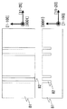
レーザストライプの位置を掘り込み領域上に作製した比較例の半導体レーザ素子を作製した。レーザストライプの位置以外については本実施形態の構成と同じである。レーザストライプを掘り込み領域16の直上に作製した構成について、素子化を行い、上記と同様にして寿命試験を行った。この場合の歩留まりは35%以下であった。この歩留まりの低下は、半導体レーザ素子に内包される歪みの違いにより引き起こされると考えられる。基板に掘り込み領域を形成しなかった場合に多数のクラックが発生したように、かなりの歪みが内包されていると考えられる。
また、歩留まりが、掘り込み領域の掘り込み幅X(図2参照)、掘り込み深さZ、および基板上に成長される窒化物半導体膜の全膜厚とに相関することを見出した。なお、窒化物半導体膜の全膜厚とは図4に示したn型GaN層40からp型GaNコンタクト層49までの窒化物半導体の全ての層を含む厚さである。
さらに、リッジを作製する位置に関しては、掘り込み領域16の端から5μm以内に作製した場合、大きく寿命試験の歩留まりを落とした。これは、掘り込み領域周辺に大きな歪みが存在しているためと考えられる。よって、レーザストライプの位置は、掘り込み領域の端から5μm以上離した領域に作製する必要がある。さらに、レーザストライプの位置を決める上で、歪みが小さい領域に作製するだけでなく、平坦性の高い領域に作製する必要がある。
11、71 窒化物半導体膜
12、72 レーザストライプ
13、73 電流狭窄用SiO2
14、74、133 p型電極
15、75、134 n型電極
16、22、52、76、82、131、1002 掘り込み領域
31、135 GaN基板上の窒化物半導体膜
32 クラック
40 n型GaN層
41 n型Al0.062Ga0.938N第一クラッド層
42 n型Al0.1Ga0.9N第二クラッド層
43 n型Al0.062Ga0.938N第三クラッド層
44 n型GaNガイド層
45 InGaN/GaN―3MQW活性層
46 p型Al0.3Ga0.7N蒸発防止層
47 p型GaNガイド層
48 p型Al0.062Ga0.938Nクラッド層
49 p型GaNコンタクト層
1003 掘りこみ領域間の領域
1004 導波路ストライプ
1005 波線状のモフォロジー
Claims (16)
- 少なくとも表面が窒化物半導体からなる基板と、当該基板の表面上に積層され且つストライプ状のレーザ光導波路構造を有する複数の窒化物半導体膜と、から成る窒化物半導体レーザ素子において、
前記基板の表面は、欠陥密度が106cm−2以下の低欠陥領域を有しており、
当該低欠陥領域には掘り込み領域が形成され、
前記複数の窒化物半導体膜は、少なくとも1層が前記基板とは組成が異なりAlを含む窒化物半導体からなり、かつ、前記掘り込み領域の上方に位置する部位の上面が凹部を有し、
前記掘り込み領域は、前記Alを含む窒化物半導体の歪みを抑制するものであり、
前記レーザ光導波路構造が、前記掘り込み領域から外れた前記低欠陥領域の上方に位置することを特徴とする窒化物半導体レーザ素子。 - 前記掘り込み領域は、ストライプ状であることを特徴とする請求項1に記載の窒化物半導体レーザ素子。
- 前記低欠陥領域に、複数の前記掘り込み領域が形成されることを特徴とする請求項1又は請求項2に記載の窒化物半導体レーザ素子。
- 前記基板の表面は、欠陥密度が106cm−2以下の前記低欠陥領域からなることを特徴とする請求項1〜請求項3のいずれかに記載の窒化物半導体レーザ素子。
- 前記レーザ光導波路構造はさらに、前記掘り込み領域の端から5μm以上離れた領域の上方に位置することを特徴とする請求項1〜請求項4のいずれかに記載の窒化物半導体レーザ素子。
- 少なくとも前記基板の表面は、欠陥密度が106cm−2以下の領域を表面に有する第1の窒化物半導体の上に形成された第2の窒化物半導体からなることを特徴とする請求項1〜請求項5のいずれかに記載の窒化物半導体レーザ素子。
- 少なくとも表面が窒化物半導体からなる基板と、当該基板の前記表面上に積層された複数の窒化物半導体膜と、から成り、前記複数の窒化物半導体膜の少なくとも一層は前記基板とは組成が異なりAlを含む窒化物半導体からなる窒化物半導体発光素子の製造方法において、
少なくとも前記表面の欠陥密度が106cm−2以下の低欠陥領域を有する前記基板の該低欠陥領域に掘り込み領域を形成する第1の工程と、
前記基板の前記表面上に前記複数の窒化物半導体膜を形成する第2の工程と、
前記第2の工程中に、Alを含む窒化物半導体膜を形成する工程とを有し、
前記Alを含む窒化物半導体膜を形成する工程は、前記掘り込み領域の上部が、前記掘り込み領域の影響を受けた凹部となるようになされ、
前記掘り込み領域は、前記Alを含む窒化物半導体の歪みを抑制するものであることを特徴とする窒化物半導体発光素子の製造方法。 - 低欠陥領域を有する第1の窒化物半導体の上に第2の窒化物半導体の層を設けて、少なくとも第2の窒化物半導体の一部を除去することにより、前記基板を作製することを特徴とする請求項7に記載の窒化物半導体発光素子の製造方法。
- 前記複数の窒化物半導体膜にストライプ状のレーザ光導波路構造を形成する第4の工程をさらに有し、
前記レーザ光導波路構造は、前記掘り込み領域から外れた領域の上方に形成することを特徴とする請求項7又は請求項8に記載の窒化物半導体発光素子の製造方法。 - 請求項7又は請求項8に記載の窒化物半導体発光素子の製造方法によって製造される窒化物半導体発光素子であって、
前記基板の表面は、欠陥密度が106cm−2以下の前記低欠陥領域からなることを特徴とする窒化物半導体発光素子。 - 請求項7又は請求項8に記載の窒化物半導体発光素子の製造方法によって製造される窒化物半導体発光素子であって、
前記掘り込み領域は、ストライプ状であり、
前記低欠陥領域に、複数の前記掘り込み領域が形成されることを特徴とする窒化物半導体発光素子。 - 前記掘り込み領域は、複数の方向に形成されることを特徴とする請求項11に記載の窒化物半導体発光素子。
- 少なくとも表面が窒化物半導体からなる基板と、当該基板の表面上に積層された複数の窒化物半導体膜と、から成る窒化物半導体ウェハにおいて、
前記基板の表面は、欠陥密度が106cm−2以下の低欠陥領域を有しており、
当該低欠陥領域には複数の掘り込み領域が形成され、
前記複数の窒化物半導体膜は、少なくとも1層が前記基板とは組成が異なりAlを含む窒化物半導体からなり、かつ、前記掘り込み領域の上方に位置する部位の上面が凹部を有し、
前記掘り込み領域は、前記Alを含む窒化物半導体の歪みを抑制するものであることを特徴とする窒化物半導体ウェハ。 - 前記基板の表面は、欠陥密度が106cm−2以下の前記低欠陥領域からなることを特徴とする請求項13に記載の窒化物半導体ウェハ。
- 前記掘り込み領域は、ストライプ状であることを特徴とする請求項13又は請求項14に記載の窒化物半導体ウェハ。
- 少なくとも表面が窒化物半導体からなる基板と、当該基板の表面上に積層された複数の窒化物半導体膜と、からなる窒化物半導体ウェハの製造方法において、
少なくとも表面が窒化物半導体からなり且つ欠陥密度が106cm−2以下の低欠陥領域を表面に有する前記基板の前記低欠陥領域に掘り込み領域を形成する第1の工程と、
前記第1の工程で前記低欠陥領域に前記掘り込み領域が形成された前記基板の表面上に、前記複数の窒化物半導体膜を形成する第2の工程と、
前記第2の工程中に、Alを含む窒化物半導体膜を形成する工程とを有し、
前記Alを含む窒化物半導体膜を形成する工程は、前記掘り込み領域の上部が、前記掘り込み領域の影響を受けた凹部となるようになされ、
前記掘り込み領域は、前記Alを含む窒化物半導体の歪みを抑制するものであることを特徴とする窒化物半導体ウェハの製造方法。
Priority Applications (4)
| Application Number | Priority Date | Filing Date | Title |
|---|---|---|---|
| JP2004183163A JP4390640B2 (ja) | 2003-07-31 | 2004-06-22 | 窒化物半導体レーザ素子、窒化物半導体発光素子、窒化物半導体ウェハおよびそれらの製造方法 |
| CN2004100556042A CN1581610B (zh) | 2003-07-31 | 2004-07-30 | 氮化物半导体发光器件及其制造方法 |
| US10/902,481 US7903708B2 (en) | 2003-07-31 | 2004-07-30 | Nitride semiconductor light-emitting device and method for fabrication thereof |
| US12/979,059 US8030110B2 (en) | 2003-07-31 | 2010-12-27 | Nitride semiconductor light-emitting device and method for fabrication thereof |
Applications Claiming Priority (2)
| Application Number | Priority Date | Filing Date | Title |
|---|---|---|---|
| JP2003204262 | 2003-07-31 | ||
| JP2004183163A JP4390640B2 (ja) | 2003-07-31 | 2004-06-22 | 窒化物半導体レーザ素子、窒化物半導体発光素子、窒化物半導体ウェハおよびそれらの製造方法 |
Related Child Applications (1)
| Application Number | Title | Priority Date | Filing Date |
|---|---|---|---|
| JP2009120220A Division JP4763818B2 (ja) | 2003-07-31 | 2009-05-18 | 窒化物半導体レーザ素子およびその製造方法 |
Publications (2)
| Publication Number | Publication Date |
|---|---|
| JP2005064469A JP2005064469A (ja) | 2005-03-10 |
| JP4390640B2 true JP4390640B2 (ja) | 2009-12-24 |
Family
ID=34106865
Family Applications (1)
| Application Number | Title | Priority Date | Filing Date |
|---|---|---|---|
| JP2004183163A Expired - Lifetime JP4390640B2 (ja) | 2003-07-31 | 2004-06-22 | 窒化物半導体レーザ素子、窒化物半導体発光素子、窒化物半導体ウェハおよびそれらの製造方法 |
Country Status (3)
| Country | Link |
|---|---|
| US (2) | US7903708B2 (ja) |
| JP (1) | JP4390640B2 (ja) |
| CN (1) | CN1581610B (ja) |
Families Citing this family (24)
| Publication number | Priority date | Publication date | Assignee | Title |
|---|---|---|---|---|
| JP3916584B2 (ja) * | 2003-04-24 | 2007-05-16 | シャープ株式会社 | 窒化物半導体レーザ装置 |
| JP3913194B2 (ja) * | 2003-05-30 | 2007-05-09 | シャープ株式会社 | 窒化物半導体発光素子 |
| JP5013661B2 (ja) * | 2004-03-31 | 2012-08-29 | 三洋電機株式会社 | 窒化物系半導体素子の製造方法及び窒化物系半導体素子 |
| JP4895488B2 (ja) * | 2004-08-26 | 2012-03-14 | シャープ株式会社 | 窒化物半導体発光素子、その製造方法、およびウエハ |
| US8368183B2 (en) | 2004-11-02 | 2013-02-05 | Sharp Kabushiki Kaisha | Nitride semiconductor device |
| JP4854275B2 (ja) * | 2004-12-08 | 2012-01-18 | シャープ株式会社 | 窒化物半導体発光素子およびその製造方法 |
| TWI316772B (en) * | 2005-09-20 | 2009-11-01 | Showa Denko Kk | Group iii nitride semiconductor light-emitting device |
| JP4963060B2 (ja) * | 2005-11-30 | 2012-06-27 | シャープ株式会社 | 窒化物系半導体レーザ素子及びその製造方法 |
| US20100085996A1 (en) * | 2006-10-17 | 2010-04-08 | Sanyo Electric Co., Ltd. | Nitride semiconductor laser device and its manufacturing method |
| JP2008244281A (ja) * | 2007-03-28 | 2008-10-09 | Sharp Corp | 窒化物半導体レーザ素子の製造方法 |
| JP2009158647A (ja) * | 2007-12-26 | 2009-07-16 | Sharp Corp | 窒化物系半導体レーザ素子およびその製造方法 |
| JP2009164233A (ja) * | 2007-12-28 | 2009-07-23 | Rohm Co Ltd | 窒化物半導体レーザ素子およびその製造方法 |
| JP2009170639A (ja) * | 2008-01-16 | 2009-07-30 | Sanyo Electric Co Ltd | 窒化物半導体レーザチップ及び窒化物半導体レーザ素子並びに窒化物半導体レーザチップの製造方法 |
| JP4966283B2 (ja) * | 2008-10-14 | 2012-07-04 | シャープ株式会社 | 半導体レーザ装置およびその製造方法 |
| JP2010219376A (ja) * | 2009-03-18 | 2010-09-30 | Sharp Corp | 窒化物半導体発光素子の製造方法 |
| JP5004989B2 (ja) | 2009-03-27 | 2012-08-22 | シャープ株式会社 | 窒化物半導体発光素子及びその製造方法、並びに、半導体光学装置 |
| JP4927121B2 (ja) * | 2009-05-29 | 2012-05-09 | シャープ株式会社 | 窒化物半導体ウェハ、窒化物半導体素子および窒化物半導体素子の製造方法 |
| US20110001126A1 (en) * | 2009-07-02 | 2011-01-06 | Sharp Kabushiki Kaisha | Nitride semiconductor chip, method of fabrication thereof, and semiconductor device |
| JP5627871B2 (ja) * | 2009-10-30 | 2014-11-19 | フューチャー ライト リミテッド ライアビリティ カンパニー | 半導体素子およびその製造方法 |
| CN103367573B (zh) * | 2013-05-23 | 2016-07-06 | 台州市一能科技有限公司 | 光电子半导体器件 |
| US9166372B1 (en) | 2013-06-28 | 2015-10-20 | Soraa Laser Diode, Inc. | Gallium nitride containing laser device configured on a patterned substrate |
| TWI504018B (zh) * | 2013-10-03 | 2015-10-11 | Univ Nat Taiwan | 半導體元件及其製造方法 |
| JP6966343B2 (ja) | 2018-01-31 | 2021-11-17 | 京セラ株式会社 | 結晶成長方法および半導体素子の製造方法 |
| CN109616560A (zh) * | 2018-11-21 | 2019-04-12 | 江西兆驰半导体有限公司 | 一种适用于氮化物外延层生长的复合衬底 |
Family Cites Families (21)
| Publication number | Priority date | Publication date | Assignee | Title |
|---|---|---|---|---|
| KR0131183B1 (ko) * | 1993-12-03 | 1998-08-17 | 양승택 | V-홈을 이용한 이종접합 구조의 박막 제조방법 |
| CN1159750C (zh) * | 1997-04-11 | 2004-07-28 | 日亚化学工业株式会社 | 氮化物半导体的生长方法 |
| US6335546B1 (en) * | 1998-07-31 | 2002-01-01 | Sharp Kabushiki Kaisha | Nitride semiconductor structure, method for producing a nitride semiconductor structure, and light emitting device |
| JP3201475B2 (ja) * | 1998-09-14 | 2001-08-20 | 松下電器産業株式会社 | 半導体装置およびその製造方法 |
| US6821805B1 (en) | 1999-10-06 | 2004-11-23 | Matsushita Electric Industrial Co., Ltd. | Semiconductor device, semiconductor substrate, and manufacture method |
| JP3809464B2 (ja) * | 1999-12-14 | 2006-08-16 | 独立行政法人理化学研究所 | 半導体層の形成方法 |
| WO2002065556A1 (en) * | 2001-02-15 | 2002-08-22 | Sharp Kabushiki Kaisha | Nitride semiconductor light emitting element and production therefor |
| JP2002284600A (ja) * | 2001-03-26 | 2002-10-03 | Hitachi Cable Ltd | 窒化ガリウム結晶基板の製造方法及び窒化ガリウム結晶基板 |
| JP3795765B2 (ja) * | 2001-04-06 | 2006-07-12 | ソニー株式会社 | 化合物半導体基板の製造方法 |
| KR100425343B1 (ko) * | 2001-04-17 | 2004-03-30 | 삼성전기주식회사 | 반도체 기판 제조방법 |
| JP4646095B2 (ja) | 2001-04-19 | 2011-03-09 | シャープ株式会社 | 半導体発光装置およびその製造方法ならびに光学式情報記録再生装置 |
| JP3864870B2 (ja) * | 2001-09-19 | 2007-01-10 | 住友電気工業株式会社 | 単結晶窒化ガリウム基板およびその成長方法並びにその製造方法 |
| JP3801125B2 (ja) * | 2001-10-09 | 2006-07-26 | 住友電気工業株式会社 | 単結晶窒化ガリウム基板と単結晶窒化ガリウムの結晶成長方法および単結晶窒化ガリウム基板の製造方法 |
| JP4388720B2 (ja) | 2001-10-12 | 2009-12-24 | 住友電気工業株式会社 | 半導体発光素子の製造方法 |
| US7498608B2 (en) * | 2001-10-29 | 2009-03-03 | Sharp Kabushiki Kaisha | Nitride-composite semiconductor laser element, its manufacturing method, and semiconductor optical device |
| US6812496B2 (en) * | 2002-01-10 | 2004-11-02 | Sharp Kabushiki Kaisha | Group III nitride semiconductor laser device |
| US7462882B2 (en) * | 2003-04-24 | 2008-12-09 | Sharp Kabushiki Kaisha | Nitride semiconductor light-emitting device, method of fabricating it, and semiconductor optical apparatus |
| JP3913194B2 (ja) * | 2003-05-30 | 2007-05-09 | シャープ株式会社 | 窒化物半導体発光素子 |
| JP4540347B2 (ja) * | 2004-01-05 | 2010-09-08 | シャープ株式会社 | 窒化物半導体レーザ素子及び、その製造方法 |
| US7157297B2 (en) * | 2004-05-10 | 2007-01-02 | Sharp Kabushiki Kaisha | Method for fabrication of semiconductor device |
| JP4322187B2 (ja) * | 2004-08-19 | 2009-08-26 | シャープ株式会社 | 窒化物半導体発光素子 |
-
2004
- 2004-06-22 JP JP2004183163A patent/JP4390640B2/ja not_active Expired - Lifetime
- 2004-07-30 CN CN2004100556042A patent/CN1581610B/zh not_active Expired - Lifetime
- 2004-07-30 US US10/902,481 patent/US7903708B2/en not_active Expired - Lifetime
-
2010
- 2010-12-27 US US12/979,059 patent/US8030110B2/en not_active Expired - Lifetime
Also Published As
| Publication number | Publication date |
|---|---|
| CN1581610B (zh) | 2012-04-11 |
| US20110136276A1 (en) | 2011-06-09 |
| CN1581610A (zh) | 2005-02-16 |
| US8030110B2 (en) | 2011-10-04 |
| US7903708B2 (en) | 2011-03-08 |
| US20050025204A1 (en) | 2005-02-03 |
| JP2005064469A (ja) | 2005-03-10 |
Similar Documents
| Publication | Publication Date | Title |
|---|---|---|
| JP3913194B2 (ja) | 窒化物半導体発光素子 | |
| JP4390640B2 (ja) | 窒化物半導体レーザ素子、窒化物半導体発光素子、窒化物半導体ウェハおよびそれらの製造方法 | |
| JP4540347B2 (ja) | 窒化物半導体レーザ素子及び、その製造方法 | |
| US7772611B2 (en) | Nitride semiconductor device with depressed portion | |
| JP4322187B2 (ja) | 窒化物半導体発光素子 | |
| JP4772314B2 (ja) | 窒化物半導体素子 | |
| JP2006134926A5 (ja) | ||
| JP5620547B2 (ja) | 窒化物半導体発光素子 | |
| JP4763818B2 (ja) | 窒化物半導体レーザ素子およびその製造方法 | |
| JP2005322786A (ja) | 窒化物半導体素子及びその製造方法 | |
| JP4679867B2 (ja) | 窒化物半導体発光素子、及びその製造方法 | |
| JP4799399B2 (ja) | 窒化物半導体発光素子 | |
| CN101867149A (zh) | 氮化物半导体发光装置的制造方法 | |
| JP4689195B2 (ja) | 半導体素子の製造方法 | |
| JP2011049583A (ja) | 窒化物半導体発光素子 | |
| JP5203412B2 (ja) | 窒化物半導体発光素子及びその製造方法 | |
| JP5530341B2 (ja) | 半導体素子及びその製造方法 | |
| JP5679699B2 (ja) | 窒化物半導体発光素子 | |
| JP4895488B2 (ja) | 窒化物半導体発光素子、その製造方法、およびウエハ |
Legal Events
| Date | Code | Title | Description |
|---|---|---|---|
| A621 | Written request for application examination |
Free format text: JAPANESE INTERMEDIATE CODE: A621 Effective date: 20060912 |
|
| RD01 | Notification of change of attorney |
Free format text: JAPANESE INTERMEDIATE CODE: A7421 Effective date: 20070926 |
|
| A977 | Report on retrieval |
Free format text: JAPANESE INTERMEDIATE CODE: A971007 Effective date: 20090305 |
|
| A131 | Notification of reasons for refusal |
Free format text: JAPANESE INTERMEDIATE CODE: A131 Effective date: 20090317 |
|
| A521 | Request for written amendment filed |
Free format text: JAPANESE INTERMEDIATE CODE: A523 Effective date: 20090518 |
|
| A131 | Notification of reasons for refusal |
Free format text: JAPANESE INTERMEDIATE CODE: A131 Effective date: 20090721 |
|
| A521 | Request for written amendment filed |
Free format text: JAPANESE INTERMEDIATE CODE: A523 Effective date: 20090730 |
|
| TRDD | Decision of grant or rejection written | ||
| A01 | Written decision to grant a patent or to grant a registration (utility model) |
Free format text: JAPANESE INTERMEDIATE CODE: A01 Effective date: 20091006 |
|
| A01 | Written decision to grant a patent or to grant a registration (utility model) |
Free format text: JAPANESE INTERMEDIATE CODE: A01 |
|
| A61 | First payment of annual fees (during grant procedure) |
Free format text: JAPANESE INTERMEDIATE CODE: A61 Effective date: 20091006 |
|
| FPAY | Renewal fee payment (event date is renewal date of database) |
Free format text: PAYMENT UNTIL: 20121016 Year of fee payment: 3 |
|
| R150 | Certificate of patent or registration of utility model |
Ref document number: 4390640 Country of ref document: JP Free format text: JAPANESE INTERMEDIATE CODE: R150 |
|
| FPAY | Renewal fee payment (event date is renewal date of database) |
Free format text: PAYMENT UNTIL: 20131016 Year of fee payment: 4 |
|
| S531 | Written request for registration of change of domicile |
Free format text: JAPANESE INTERMEDIATE CODE: R313531 |
|
| R350 | Written notification of registration of transfer |
Free format text: JAPANESE INTERMEDIATE CODE: R350 |
|
| RD03 | Notification of appointment of power of attorney |
Free format text: JAPANESE INTERMEDIATE CODE: R3D03 |
|
| S111 | Request for change of ownership or part of ownership |
Free format text: JAPANESE INTERMEDIATE CODE: R313113 |
|
| S111 | Request for change of ownership or part of ownership |
Free format text: JAPANESE INTERMEDIATE CODE: R313113 |
|
| R371 | Transfer withdrawn |
Free format text: JAPANESE INTERMEDIATE CODE: R371 |
|
| S111 | Request for change of ownership or part of ownership |
Free format text: JAPANESE INTERMEDIATE CODE: R313113 |
|
| R350 | Written notification of registration of transfer |
Free format text: JAPANESE INTERMEDIATE CODE: R350 |
|
| EXPY | Cancellation because of completion of term |