JP4402183B2 - Image forming apparatus - Google Patents
Image forming apparatus Download PDFInfo
- Publication number
- JP4402183B2 JP4402183B2 JP8865098A JP8865098A JP4402183B2 JP 4402183 B2 JP4402183 B2 JP 4402183B2 JP 8865098 A JP8865098 A JP 8865098A JP 8865098 A JP8865098 A JP 8865098A JP 4402183 B2 JP4402183 B2 JP 4402183B2
- Authority
- JP
- Japan
- Prior art keywords
- image forming
- forming apparatus
- width
- protective layer
- layer
- Prior art date
- Legal status (The legal status is an assumption and is not a legal conclusion. Google has not performed a legal analysis and makes no representation as to the accuracy of the status listed.)
- Expired - Fee Related
Links
Images



Landscapes
- Discharging, Photosensitive Material Shape In Electrophotography (AREA)
- Cleaning In Electrography (AREA)
Description
【0001】
【発明の属する技術分野】
本発明は、複写機、レーザープリンタ及びファックスなどの電子写真方式の画像形成装置に関するものである。
【0002】
【従来の技術】
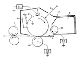
一般的な電子写真方式の画像形成装置を図2に示す。以下に簡単に図を説明する。画像形成装置内には、回転自在に軸支され矢印方向に回転する静電潜像を担持するための像担持体、即ち感光体21が配置され、その外周部に画像形成手段が配置される。
【0003】
感光体21を均一に帯電する一次帯電器2と色分解された光像またはこれに相当する光像を照射し、感光体21上に静電潜像を形成する。例えば、レーザービーム露光装置などからなる露光手段Lと、感光体21上の静電潜像を可視画像とする現像装置3aとを具備する。
【0004】
感光体21上の可視画像、即ちトナー像は、転写ローラー4によって搬送された転写材Pに転写される。
【0005】
上述したような構成の電子写真複写装置による画像の形成工程を簡単に説明する。まず、帯電器2及び像露光手段Lが作動されることにより前記感光体21の外周面上に原稿に忠実な静電潜像が形成され、該静電潜像は、現像装置3aに収納されている現像剤であるトナーにて現像される。一方、転写ローラー4へと送給された転写材Pは、転写ローラー4の回転に伴って、前記感光体21の外周面上に形成されたトナー像に当接される。該トナー像は、前記転写ローラー4の帯電作用により前記転写材P上に転写される。転写が終了すると、熱ローラー定着器5を介して機外へと排出される。一方感光体21上の残留トナーはクリーナ6にて除去され、感光体21には次の画像形成プロセスが施される。
【0006】
感光体には運用される電子写真プロセスに応じた所要の感度、電気特性更には光学特性を備えていることが要求されるが、更に、先記のごときプロセスにより繰り返し使用される感光体にあっては、感光体の表面層、即ち支持体より最も隔離する層には、コロナ帯電、トナー現像、紙への転写及びクリーニング処理などの電気的及び機械的外力が直接に加えられるために、それらに対する耐久性が要求される。具体的には、摺擦による表面の摩耗やキズの発生、またコロナ帯電時に発生するオゾンによる表面の劣化などに対する耐久性が要求されている。一方、トナーの現像及びクリーニングの繰り返しによる表面層へのトナー付着という問題もあり、これに対しては表面層のクリーニング性を向上することが求められている。
【0007】
上記のような表面層に要求される特性を満たすために、樹脂を主成分とする表面保護層を設ける試みがなされている。例えば、特開昭57−207258号公報や特開昭53−103741号公報などに提案されているように硬化型樹脂を主成分とする保護層を用い、硬度及び耐摩耗性の向上が図られている。しかしながら、これら硬化型の樹脂を表面保護層として用いた場合、特に下層となる感光層が、これも樹脂を主成分とする有機感光体の場合には、硬化性樹脂の硬化時の収縮によって保護層または感光層にキレツが入り易いという問題があり、いまだに有機感光体において、これら硬化性樹脂を用いた保護層の実用化を妨げていた。また、感光体の保護層に要求される特性は高い硬度や耐摩耗性などの表面物性の他に、保護層自体の抵抗コントロールが重要な課題となる。即ち、保護層の抵抗が高過ぎる場合には帯電−露光を繰り返す電子写真プロセスにおいて、保護層自体に電荷が蓄積していく、いわゆる残留電位の増加が起こり、そのため感光体の繰り返し使用時に電位が安定しないため、画像も不安定になる。また、該抵抗が低過ぎる場合には静電潜像が保護層中を面方向に流れて、画像がにじむ及びボケるなどの問題が発生する。
【0008】
これらの問題を解決するために、例えば特開昭57−30843号公報に提案されているように、導電性微粒子として金属酸化物を添加して抵抗を制御した保護層が提案されている。
【0009】
これにより先記した問題は回避された。しかし、新たな問題が表出した。感光体を放電手段を用いて帯電させながら耐久すると、表面は帯電による分解やオゾンやNOxなどの帯電生成物による分解、また帯電生成物そのものの吸着が生じ感光体の表面エネルギーは著しく高くなる。このため、表面滑性のダウン、転写効率のダウン、また高温高湿環境下での耐久放置後の画像流れの発生などの問題が発生した。
【0010】
【発明が解決しようとする課題】
この問題点に対して、感光体表面を微量研磨し、表面の帯電生成物や分解物のみを積極的に除去する方法が提案されている。具体的には、感光体表面に当接するクリーニング手段の上流側及び/または下流側で感光体に当接し、感光体に対して回転速度差を有して回転する研磨装置を配設する方法である。研磨装置としては磁性体ブラシローラーや弾性ゴムローラーなどが用いられている。この方法を用いることで転写効率ダウンや画像流れに対しては効果が確認されている。しかし、表面滑性に対しては、効果の充分な確認は行われていなかった。
【0011】
本発明者らは、研磨装置を具備し表面滑性が良好になっていると考えられる系と具備していない系に関し、高温高湿環境下での耐久試験を行った。そうしたところ、クリーニング不良が両者において発生してしまった。不良発生時の枚数という点では研磨装置を具備している系に若干の効果は認められたものの、大きな差異ではなかった。
【0012】
本発明の目的は、感光体表面が削れにくいため帯電生成物などの影響を受け易い、保護層を有する感光体を用いた画像形成装置において、高温高湿環境下耐久でクリーニング不良の発生しない画像形成装置を提供することにある。
【0013】
【課題を解決するための手段】
上記目的は本発明の画像形成装置を用いることにより達成される。即ち、本発明は、移動する電子写真感光体の表面をこれに当接させた接触帯電部材で接触帯電し、次いで像露光及び現像を行って該電子写真感光体の表面に現像像を形成し、該現像像を該電子写真感光体の表面から転写材に転写した後、該電子写真感光体の表面をこれに当接させたクリーニング部材でクリーニングし、該電子写真感光体の表面を再使用する画像形成装置であって、該電子写真感光体が硬化性樹脂を含有する保護層を表面に有しており、該接触帯電部材が放電手段である画像形成装置において、
該保護層の塗布幅、該クリーニング部材の幅及び該接触帯電部材の幅が、以下の関係(i)及び(ii)
(i) クリーニング部材の幅<接触帯電部材の幅
(ii) 接触帯電部材の幅+2mm≦保護層の塗布幅
を満足することを特徴とする画像形成装置である。
【0015】
【発明の実施の形態】
本発明の詳細を以下に示す。
【0016】
本発明者らは、接触帯電での高温高湿環境下耐久でクリーニング不良の発生するメカニズムを以下のように考えている。
【0017】
感光体の保護層表面の滑性について詳しく調べてみると、接触帯電部材の当接している箇所とそうでない箇所では、滑り性に大きな差が生じていることが分った。このときクリーニング部材が先記した両方の場所にまたがって当接していると、クリーニング部材と感光体表面の摩擦応力の異なる場所が同一クリーニング部材中に存在することになり、クリーニング部材に応力歪みを引き起こすものと考えられる。ゆえに、クリーニング部材の歪み変位量が最大となる部分を起点としてクリーニング不良が発生する。しかし、本発明者らは検討を重ねるうち、クリーニング不良の発生箇所が歪み変位量最大となる部分以外でも起こり得ることを確認した。この原因に関しては、まだメカニズム解明は行われていない。
【0018】
本発明者らは当初、歪み変位量最大となる部分のクリーニング不良対策として、本発明の装置の提供を考えた。つまり、接触帯電部材の幅より、クリーニング部材の幅を短くすることで、クリーニング部材の歪みの発生しない装置を考案した。
【0021】
本発明における保護層について以下に説明する。
【0022】
本発明の保護層に用いることのできる結着樹脂としては、ポリカーボネート樹脂、ポリエステル樹脂、ポリアリレート樹脂、ポリスチレン樹脂、ポリエチレン樹脂、ポリプロピレン樹脂、ポリウレタン樹脂、アクリル樹脂、エポキシ樹脂、シリコーン樹脂、セルロース樹脂、ポリ塩化ビニル樹脂、ホスファゼン樹脂、メラミン樹脂及び塩化ビニル−酢酸ビニル共重合体などが挙げられる。これらの樹脂は単独で用いることも、2種以上を組み合わせて用いることもできる。
【0023】
上記樹脂の中でも、保護層の表面硬度、耐摩耗性、更に微粒子の分散性及び分散後の安定性の点から硬化性樹脂を用いることが好ましい。即ち、熱または光によって硬化するモノマーまたはオリゴマーを含有する溶液に前述の導電性粒子及びフッ素原子含有樹脂粒子を分散させて保護層用の塗工液とし、この溶液を感光層上に塗工後、硬化させて形成した保護層は、分散性、硬度及び耐摩耗性などの点でより好ましい。
【0024】
熱または光によって硬化するモノマーまたはオリゴマーとは、例えば分子の末端に熱または光のエネルギーによって重合反応を起こす官能基を有するもので、このうち分子の構造単位の繰り返しが2〜20程度の比較的大きな分子がオリゴマー、それより小さいものがモノマーである。該重合反応を起こす官能基としてはアクリロイル基、メタクリロイル基及びビニル基などの炭素−炭素二重結合を有する基、シラノール基、更に環状エーテル基などの開環重合を起こすもの、またはフェノールとホルムアルデヒドのように二種類以上の分子が反応して重合を起こすものなどが挙げられる。
【0025】
本発明における保護層中には導電性粒子を混入させてもよい。
【0026】
導電性粒子としては、金属、金属酸化物及びカーボンブラックなどが挙げられる。金属としては、アルミニウム、亜鉛、銅、クロム、ニッケル、ステンレス及び銀など、またはこれらの金属をプラスチックの粒子の表面に蒸着したものなどが挙げられる。金属酸化物としては、酸化亜鉛、酸化チタン、酸化スズ、酸化アンチモン、酸化インジウム、酸化ビスマス、スズをドープした酸化インジウム、アンチモンをドープした酸化スズ及びアンチモンをドープした酸化ジルコニウムなどが挙げられる。これらは単独で用いることも、2種以上を組み合わせて用いることもできる。2種以上を組み合わせて用いる場合は、単に混合しても、固溶体や融着の形にしてもよい。
【0027】
本発明に用いられる導電性粒子の平均粒径は保護層の透明性の点で0.3μm以下であることが好ましく、特には0.1μm以下であることが好ましい。
【0028】
また、本発明においては上述したような導電性粒子の中でも、透明性などの点で金属酸化物を用いることが特に好ましい。
【0029】
更に、本発明における保護層中にはフッ素原子含有樹脂粒子を含有することができる。
【0030】
フッ素原子含有樹脂粒子としては、四フッ化エチレン樹脂、三フッ化塩化エチレン樹脂、六フッ化エチレンプロピレン樹脂、フッ化ビニル樹脂、フッ化ビニリデン樹脂、二フッ化二塩化エチレン樹脂及びこれらの共重合体のなかから1種あるいは2種以上を適宜選択するのが好ましいが、特に、四フッ化エチレン樹脂及びフッ化ビニリデン樹脂が好ましい。樹脂粒子の分子量や粒子の粒径は、適宜選択することができ、特に制限されるものではない。
【0031】
本発明においては、導電性粒子及びフッ素原子含有樹脂粒子を共に樹脂溶液中でお互いの粒子を凝集させないように、導電性粒子の表面をフッ素原子含有化合物で表面処理する。表面処理を行うことにより、表面処理を行わない場合に比べて、樹脂溶液中での導電性粒子とフッ素原子含有樹脂粒子の分散性及び分散安定性が格段に向上した。また、フッ素原子含有化合物で表面処理を施した導電性粒子とフッ素原子含有樹脂粒子とを溶剤に溶かした結着樹脂中に分散することによって分散粒子の二次粒子の形成もなく、経時的にも非常に安定した分散性の良い塗工液が得られた。
【0032】
本発明において導電性粒子をフッ素原子含有化合物によって表面処理する際、用いることのできるフッ素原子含有化合物としては含フッ素シランカップリング剤、フッ素変性シリコーンオイル、フッ素系界面活性剤などが挙げられる。以下に、それぞれの好ましい化合物を例示するが、これらの化合物に限定されるものではない。
【0033】
含フッ素シランカップリング剤の好ましいものとしては、
CF3 CH2 CH2 Si(OCH3 )3 、
C4 F9 CH2 CH2 Si(OCH3 )3 、
C6 F13CH2 CH2 Si(OCH3 )3 、
C8 F17CH2 CH2 Si(OCH3 )3 、
C8 F17CH2 CH2 Si(OCH2 CH2 OCH3 )3 、
C10F21Si(OCH3 )3 、
C6 F13CONHSi(OCH3 )3 、
C8 F17CONHSi(OCH3 )3 、
C7 F15CONHCH2 CH2 CH2 Si(OCH3 )3 、
C7 F15CONHCH2 CH2 CH2 Si(OC2 H5 )3 、
C7 F15COOCH2 CH2 CH2 Si(OCH3 )3 、
C7 F15COSCH2 CH2 CH2 Si(OCH3 )3 、
C8 F17SO2 NHCH2 CH2 CH2 Si(OC2 H5 )3 、
【0034】
【化1】

C10F21CH2 CH2 SCH2 CH2 Si(OCH3 )3 、
【0035】
【化2】
【化3】
【0037】
フッ素変性シリコーンオイルの好ましいものとしては、
【0038】
【化4】
【0039】
フッ素系界面活性剤の好ましいものとしては、
X−SO2 NRCH2 COOH、
X−SO2 NRCH2 CH2 O(CH2 CH2 O)n H(n=5、10、15)、
X−SO2 N(CH2 CH2 CH2 OH)2 、
X−RO(CH2 CH2 O)n (n=5、10、15)、
X−(RO)n (n=5〜20)、
X−(RO)n R(n=5〜20)、
【0040】
【化5】
【化6】
【化7】
【化8】
【0044】
導電性粒子の表面処理方法は、以下の通りである。まず、導電性粒子と表面処理剤とを適当な溶剤中で混合、分散し、表面処理剤を導電性粒子表面に付着させる。分散の手段としてはボールミル及びサンドミルなどの通常の分散手段を用いることができる。次に、この分散溶液から溶剤を除去し、導電性粒子表面に表面処理剤を固着させればよい。また必要に応じて、この後更に熱処理を行ってもよい。また、処理液中には反応促進のための触媒を添加してもさしつかえない。更に、必要に応じて表面処理後の導電性粒子に更に粉砕処理を施してもよい。
【0045】
導電性粒子に対するフッ素原子含有化合物の割合は、粒子の粒径にも影響を受けるが、表面処理済の導電性粒子全重量に対し、1〜65重量%であることが好ましく、より好ましくは10〜50重量%である。
【0046】
前記保護層中の導電性金属酸化物粒子の割合は、直接的に保護層の抵抗を決定する要因のひとつであり、保護層の抵抗は1010〜1015ohm・cmの範囲であることが好ましい。
【0047】
前記保護層中のフッ素原子含有樹脂粒子の割合は、保護層全重量に対し5〜70重量%が好ましく、より好ましくは10〜60重量%である。フッ素原子含有樹脂粒子の割合が70重量%より多いと保護層の機械的強度が低下し易く、フッ素原子含有樹脂粒子の割合が5重量%より少ないと保護層表面の離型性、保護層の耐摩耗性や耐傷性が充分ではなくなることがある。
【0048】
本発明においては、分散性、結着性及び耐候性を更に向上させる目的で、前記保護層中にラジカル補足剤や酸化防止剤などの添加物を加えてもよい。
【0049】
本発明に用いる保護層の膜厚は0.2〜10μmの範囲が好ましく、より好ましくは0.5〜6μmの範囲である。
【0050】
次に、感光層について説明する。本発明に用いる電子写真感光体の感光層の構成は電荷発生物質と電荷輸送物質の双方を同一の層に含有する単層型、あるいは電荷発生物質を含有する電荷発生層と電荷輸送物質を含有する電荷輸送層を導電性支持体上に積層した積層型のいずれかである。以下に積層型の感光層について説明する。
【0051】
積層型の感光層の構成としては、導電性支持体上に電荷発生層、電荷輸送層をこの順に積層したものと、逆に電荷輸送層、電荷発生層の順に積層したものがある。
【0052】
本発明で用いる導電性支持体は導電性を有するものであれば、いずれのものでもよく、例えばアルミニウム、銅、クロム、ニッケル、亜鉛及びステンレスなどの金属をドラムまたはシート状に成形したもの、アルミニウムや銅などの金属箔をプラスチックフィルムにラミネートしたもの、アルミニウム、酸化インジウム及び酸化スズなどをプラスチックフィルムに蒸着したもの、導電性物質を単独または結着樹脂と共に塗布して導電層を設けた金属、プラスチックフィルム及び紙などが挙げられる。
【0053】
積層型感光体の電荷輸送層はピラゾリン化合物、ヒドラゾン化合物、スチリル化合物及びトリアリールアミン化合物などの電荷輸送物質を成膜性を有する樹脂に溶解させた塗工液を用いて形成される。
【0054】
このような成膜性を有する樹脂としてはポリエステル、ポリカーボネート、ポリスチレン及びポリメタクリル酸エステルなどが挙げられる。電荷輸送層の厚さは5〜40μm、好ましくは10〜30μmである。
【0055】
積層型感光体の電荷発生層はスーダンレッド及びダイアンブルーなどのアゾ顔料;ピレンキノン及びアントアントロンなどのキノン顔料、キノシアニン顔料、ペリレン顔料、インジゴ及びチオインジゴなどのインジゴ顔料;及びフタロシアニン顔料などの電荷発生物質をポリビニルブチラール、ポリスチレン及びポリ酢酸ビニル及びアクリル樹脂などの結着樹脂に分散させて、この分散液を塗工するか、前記顔料を真空蒸着することによって形成する。このような電荷発生層の膜厚は、好ましくは5μm以下、より好ましくは0.05〜3μmである。
【0056】
本発明においては、感光層と保護層の接着性をより向上させるために、これらの層の間に0.1〜5μm程度の厚さを有する中間層を設けることができる。
【0057】
また、本発明においては、導電性支持体と感光層の間にバリアー機能と接着機能をもつ下引層を設けることができる。下引層は、カゼイン、ポリビニルアルコール、ニトロセルロース、エチレン−アクリル酸コポリマー、アルコール可溶アミド、ポリウレタン及びゼラチンなどによって形成できる。下引層の膜厚は0.1〜0.3μmが好ましい。
【0058】
本発明の画像形成装置は、複写機、レーザープリンタ、LEDプリンタ及び液晶シャッター式プリンタなどの電子写真装置一般に適用し得るだけでなく、更に電子写真技術を応用したディスプレー、記録、軽印刷、製版及びファクシミリなどの装置にも幅広く適用し得るものである。
【0059】
以下に、具体的実施例を挙げて、本発明を更に詳しく説明する。
【0060】
【実施例】
(実施例1)
アルミニウムシリンダー(略φ60mm×360mm)上に、アルコール可溶性ポリアミド樹脂(アミランCM−8000、東レ(株)製)10部(重量部、以下同様)及びメトキシメチル化6ナイロン樹脂(トレジンEF−30T、帝国科学(株)製)30部をメタノール150部及びブタノール150部の混合溶媒中に溶解した調合液を浸漬コーティング法で塗布し、90℃で10分間乾燥させて、膜厚1μmの下引層を形成した。
【0061】
次に、下記構造式
【0062】
【化9】
【0063】
次に、下記構造式
【0064】
【化10】
【0065】
次に、保護層用の調合液を下記の手順により作成した。
【0066】
平均粒径0.02μmのアンチモン含有酸化スズ微粒子(T−1、三菱マテリアル(株)製)100部、(3,3,3−トリフルオロプロピル)トリメトキシシラン(チッソ(株)製)10部及びエタノール300部を攪拌装置で48時間攪拌した後、溶液を濾過・洗浄後、乾燥し、更に150℃で2時間熱処理を行い、微粒子の表面処理を行った。
【0067】
次に、下記構造式
【0068】
【化11】
【0069】
この調合液を用いて前記電荷輸送層上に浸漬コーティング法で成膜し、乾燥後メタルハライドランプにて250mW/cm2 の光強度で60秒間紫外線照射して、膜厚3μmの保護層を形成し、感光体を得た。
【0070】
この感光体を図3に示される画像形成装置であるレーザービームプリンタにセットした。以下に図3の画像形成装置について説明する。
【0071】
前記感光ドラム31は矢印の方向に120[mm/sec]または30[mm/sec]の周速度をもって回転駆動され、まず、その表面は接触帯電手段としての一次帯電ローラー32によって、暗部電位VDとして−700[v]に一様帯電される。次に、第1の画像情報に応じてON/OFF制御されたレーザービーム33による走査露光が施され、明部電位VLとして−100[v]の第1の静電潜像が形成される。このように形成された静電潜像は、現像装置34により、現像、可視像化されるが、この現像装置34は、第1色目のトナーとしてイエロートナーが内包された第1の現像装置34a、第2色目のトナーとしてマゼンタトナーが内包された第2の現像装置34b、第3色目のトナーとしてシアントナーが内包された第3の現像装置34c、第4色目のトナーとしてブラックトナーが内包された第4の現像装置34dを一体化した構成となっており、まず前記第1の静電潜像は、第1色目のトナーとしてイエロートナーが内包された第1の現像装置34aにより現像、可視化される。現像方法としては、ジャンピング現像、2成分現像法、FEED現像法などが用いられ、イメージ露光と反転現像とを組み合わせて用いられることが多い。
【0072】
可視化された第1色目のトナー像は、回転駆動される第2の像担持体としての中間転写体35と対向する第1の転写部位36aにおいて、中間転写体35表面に静電転写(一次転写)される。前記中間転写体35は、転写材の長さよりも若干長い周長を有し、前記感光ドラム31に対して所定の押圧力をもって圧接されつつ、感光ドラムの周速度と略等速の周速度をもって感光ドラム31の回転方向に対して順方向に回転駆動される。そして、前記のように感光ドラム31表面に形成されたトナー像は、高圧電源37により前記中間転写体35に対して、トナーの帯電極性とは逆極性の電圧(一次転写バイアス)が印加されることにより、中間転写体35表面に静電転写(一次転写)される。
【0073】
なお、一次転写が終了した感光ドラム31表面に若干量残存するトナーは、クリーニング装置38によって除去される。
【0074】
続いて、前記工程を3回繰り返し、その都度、マゼンタトナーにより現像された第2色目のトナー像、シアントナーにより現像された第3色目のトナー像、ブラックトナーにより現像された第4色目のトナー像が順次中間転写体35表面に転写、積層される。
【0075】
その後、中間転写体35表面に対して離間状態にあった転写ベルト39が所定の押圧力をもって中間転写体35表面に圧接、回転駆動される。前記転写ベルト39は、バイアスローラー39a、及びテンションローラー39bによって支持され、前記バイアスローラー39aに対しては、高圧電源40により、トナーの帯電極性とは逆極性の電圧(二次転写バイアス)が印加されることにより、第2の転写部位36bに所定のタイミングで搬送されてくる転写材P表面に、中間転写体35表面に形成されたトナー像が一括転写(二次転写)され、この転写材Pは不図示の定着装置へと搬送され、永久画像として定着された後、機外へと排出される。
【0076】
そして、二次転写が終了した中間転写体35表面に若干量残存するトナーは、所定のタイミングで中間転写体35表面に対して当接状態となるクリーニング装置41により除去される。
【0077】
次に、本実施例で用いたトナーについて説明する。
【0078】
本実施例で用いたトナーは低軟化点物質を5〜30[重量%]含み、その形状係数SF1が100〜150、形状係数SF2が100〜140、粒径が5〜7[μm]の実質的球形である非磁性一成分トナーである。
【0079】
なお、前記形状係数SF1とは図4に示すように、球状物質の形状の丸さの割合を示す数値であり、球状物質を2次元平面上に投影してできる楕円状図形の最大長MXLNGの二乗を図形面積AREAで割って、100π/4を乗じた値で表される。
【0080】
つまり次式、
SF1={(MXLNG)2 /AREA}×(100π/4)
によって定義されるものである。
【0081】
前記トナー52の概略構成図を図5に示すが、このようなトナーはその製造法上、略球形となり、本実施例においては、コア52aにエステル系ワックスを内包し、樹脂層52bにスチレン−ブチルアクリレート、表層52cにスチレン−ポリエステルという構成から成るトナーを用いた。その比重は約1.05である。
【0082】
前述のように、コア52aにワックスを内包することで、定着工程でのオフセット防止効果が得られるとともに、表層52aに樹脂層を設けることにより帯電効率のアップを図ることが可能となり、更にトリボ(Q/M)安定化のためにオイル処理シリカを外添することによって、前記トナーのトリボはおよそ−20[μC/g]であった。
【0083】
次に、本実施例で用いた弾性ブレード及び潤滑材塗布機構を備えるクリーニング装置38について、図6を用いて説明する。
【0084】
図6において、38aはクリーニングブレード、38bはトナー捕集シート、38cは廃トナー回収容器である。
【0085】
先に述べたように、一次転写が終了した感光ドラム31表面に若干量残存するトナーは、クリーニング装置38を構成するクリーニングブレード38aによって感光ドラム31から除去され、廃トナー捕集シート38bによってクリーニング装置38の外部へ飛散すること無く、廃トナー回収容器38cに格納される。
【0086】
クリーニングブレード38aは板金38fの先端部に一体的に保持されたポリウレタンゴムから成り、感光ドラム31に対して所定の侵入量、設定角の条件で当接されている。
【0087】
先記の画像形成装置の中で図1に示されるような感光体表面の保護層の塗工幅とクリーニングブレードの幅と一次帯電ローラーの幅の関係は表1に示す通りの関係であった。
【0088】
このレーザービームプリンタを高温高湿環境下(30℃、80%RH)に設置し、耐久試験を行い、クリーニング状況について検討を行った。その結果を表1に示す。
【0089】
(参考例1)
実施例1におけるクリーニングブレード幅が一次帯電ローラー幅に対して両端部で1mmずつ長くなったこと以外は、実施例1と同様の感光体及び同様の条件で評価を行った。その結果を表1に示す。
【0090】
(参考例2)
実施例1におけるクリーニングブレード幅と一次帯電ローラー幅が同じであること以外は、実施例1と同様の感光体及び同様の条件で評価を行った。その結果を表1に示す。
【0091】
(比較例1)
実施例1におけるクリーニングブレード幅が一次帯電ローラー幅より10mm長いこと以外は、実施例1と同様の感光体及び同様の条件で評価を行った。その結果を表1に示す。
【0092】
(比較例2)
比較例1における感光体の保護層がないこと以外は、比較例1と同様の条件で評価を行った。その結果を表1に示す。表1に記載されているようにクリーニング不良の発生はなかったが、耐久中2K枚当りから感光体表面に生じた傷起因の画像上黒スジが発生した。
【0093】
(比較例3)
実施例1における感光体の保護層がないこと以外は、実施例1と同様の条件で評価を行った。その結果を表1に示す。比較例2同様クリーニング不良の発生はないが、画像上黒スジが発生した。
【0094】
(比較例4)
参考例1におけるクリーニングブレード幅が更に両端部で3mmずつ長いこと以外は、参考例1と同様の感光体及び同様の条件で評価を行った。その結果を表1に示す。
【0095】
【表1】
【発明の効果】
以上説明したように、本発明の移動する電子写真感光体の表面をこれに当接させた接触帯電部材で接触帯電し、次いで像露光及び現像を行って該電子写真感光体の表面に現像像を形成し、該現像像を該電子写真感光体の表面から転写材に転写した後、該電子写真感光体の表面をこれに当接させたクリーニング部材でクリーニングし、該電子写真感光体の表面を再使用する画像形成装置であって、該電子写真感光体が硬化性樹脂を含有する保護層を表面に有しており、該接触帯電部材が放電手段である画像形成装置において、
該保護層の塗布幅、該クリーニング部材の幅及び該接触帯電部材の幅が、以下の関係(i)及び(ii)
(i) クリーニング部材の幅<接触帯電部材の幅
(ii) 接触帯電部材の幅+2mm≦保護層の塗布幅
を満足することを特徴とする画像形成装置を用いることで、高温高湿環境下で耐久してもクリーニング不良が発生することなく、高品質な機械を提供することができる。
【図面の簡単な説明】
【図1】本発明におけるクリーニング部材の幅、接触帯電部材の幅及び保護層の塗布幅を示す模式図。
【図2】一般的な電子写真方式の画像形成装置であるレーザービームプリンタの概略図。
【図3】実施例で用いた画像形成装置であるレーザービームプリンタの概略図。
【図4】トナーの形状係数SF1を説明する図。
【図5】実施例で用いたトナーの概略構成図。
【図6】本実施例で用いたクリーニング装置の概略図。
【符号の説明】
21 像担持体(感光体ドラム)
2 接触帯電部材(一次帯電ローラー)
L 走査露光光(レーザー光)
3 現像装置
3a 現像スリーブ
4 転写ローラー
5 定着装置
6 クリーニング装置
6a クリーニング部材(ゴムブレード)
20 レーザービームプリンタ本体
P 転写材(紙)
S1,S2,S3 高圧電源
31 像担持体(感光体ドラム)
32 一次帯電ローラー
33 レーザー光
34 現像装置
34a イエロー現像器
34b マゼンタ現像器
34c シアン現像器
34d ブラック現像器
35 中間転写体
38 クリーニング装置
38a クリーニングブレード
38b 廃トナー捕集シート
38c 廃トナー回収容器
38f 板金
39 転写ベルト
41 中間転写体用クリーニングローラー
52 トナー
52a コア
52b 樹脂層
52c 表層[0001]
BACKGROUND OF THE INVENTION
The present invention relates to an electrophotographic image forming apparatus such as a copying machine, a laser printer, and a fax machine.
[0002]
[Prior art]
A general electrophotographic image forming apparatus is shown in FIG. The figure is briefly described below. In the image forming apparatus, an image bearing member, ie, a
[0003]
PhotosensitivityBody 21The
[0004]
The visible image on the
[0005]
An image forming process by the electrophotographic copying apparatus having the above-described configuration will be briefly described. First, by operating the
[0006]
The photoreceptor is required to have required sensitivity, electrical characteristics, and optical characteristics according to the electrophotographic process to be used. Since the surface layer of the photoreceptor, that is, the layer most isolated from the support, is directly subjected to electrical and mechanical external forces such as corona charging, toner development, transfer to paper, and cleaning processing, these Durability is required. Specifically, durability against surface abrasion and scratches due to rubbing and surface degradation due to ozone generated during corona charging is required. On the other hand, there is a problem that toner adheres to the surface layer due to repeated development and cleaning of the toner.
[0007]
In order to satisfy the characteristics required for the surface layer as described above, an attempt is made to provide a surface protective layer mainly composed of a resin. For example, as proposed in JP-A-57-207258, JP-A-53-103741, etc., a protective layer mainly composed of a curable resin is used to improve the hardness and wear resistance. ing. However, when these curable resins are used as a surface protective layer, particularly when the underlying photosensitive layer is also an organic photoreceptor having a resin as a main component, it is protected by shrinkage during curing of the curable resin. There is a problem that the layer or the photosensitive layer tends to be crisp, and still has prevented the practical use of the protective layer using these curable resins in the organic photoreceptor. In addition to the surface properties such as high hardness and wear resistance, the properties required for the protective layer of the photosensitive member are important issues for resistance control of the protective layer itself. That is, when the resistance of the protective layer is too high, in the electrophotographic process in which charging and exposure are repeated, charges accumulate in the protective layer itself, so-called residual potential increases. Since it is not stable, the image becomes unstable. When the resistance is too low, the electrostatic latent image flows in the surface direction through the protective layer, causing problems such as blurring and blurring of the image.
[0008]
In order to solve these problems, for example, as proposed in JP-A-57-30843, a protective layer in which resistance is controlled by adding a metal oxide as conductive fine particles has been proposed.
[0009]
As a result, the above-mentioned problems were avoided. However, a new problem has emerged. When the photoreceptor is endured while being charged by using a discharging means, the surface is decomposed by charging, decomposed by a charged product such as ozone or NOx, and the charged product itself is adsorbed, and the surface energy of the photoreceptor is remarkably increased. For this reason, problems such as a decrease in surface smoothness, a decrease in transfer efficiency, and an image flow after standing in a high temperature and high humidity environment have occurred.
[0010]
[Problems to be solved by the invention]
In order to solve this problem, a method has been proposed in which a small amount of the surface of the photoconductor is polished to positively remove only charged products and decomposition products on the surface. Specifically, on the upstream side and / or downstream side of the cleaning means that contacts the surface of the photoreceptor.PhotoconductorAnd a polishing device that rotates with a difference in rotational speed with respect to the photosensitive member. As a polishing apparatus, a magnetic brush roller, an elastic rubber roller, or the like is used. Use of this method has been confirmed to be effective in reducing transfer efficiency and image flow. However, sufficient confirmation of the effect on the surface slipperiness has not been performed.
[0011]
The present inventors conducted an endurance test in a high-temperature and high-humidity environment with respect to a system that is equipped with a polishing apparatus and is considered to have good surface lubricity and a system that is not. As a result, a cleaning failure occurred in both. Although a slight effect was recognized in the system equipped with the polishing apparatus in terms of the number of defects when the defect occurred, it was not a big difference.
[0012]
An object of the present invention is to have a protective layer that is easily affected by a charged product because the surface of the photoreceptor is hard to be scraped.PhotoconductorIn the image forming apparatus using the above, an image forming apparatus that is durable under a high temperature and high humidity environment and that does not cause defective cleaning is provided.
[0013]
[Means for Solving the Problems]
The above object is achieved by using the image forming apparatus of the present invention. That is, according to the present invention, the surface of a moving electrophotographic photosensitive member is contact-charged by a contact charging member in contact with the surface, and then image exposure and development are performed to form a developed image on the surface of the electrophotographic photosensitive member. After the developed image is transferred from the surface of the electrophotographic photosensitive member to a transfer material, the surface of the electrophotographic photosensitive member is cleaned with a cleaning member in contact with the surface, and the surface of the electrophotographic photosensitive member is reused. An image forming apparatus, wherein the electrophotographic photosensitive member has a protective layer containing a curable resin on a surface thereof.The contact charging member is a discharging means.In the image forming apparatus
The application width of the protective layer, the width of the cleaning member, and the width of the contact charging member have the following relationships (i) and (ii)
(I) width of cleaning member <width of contact charging member
(Ii) Contact charging member width + 2 mm ≦ protection layer coating width
An image forming apparatus characterized by satisfying the above.
[0015]
DETAILED DESCRIPTION OF THE INVENTION
Details of the present invention are shown below.
[0016]
The present inventors consider the mechanism of occurrence of defective cleaning in a high temperature and high humidity environment with contact charging as follows.
[0017]
Examining in detail the slipperiness of the surface of the protective layer of the photoreceptor, it was found that there was a large difference in slipperiness between the place where the contact charging member was in contact and the place where it was not. At this time, if the cleaning member is in contact with both of the above-mentioned locations, the locations where the cleaning member and the surface of the photosensitive member have different frictional stresses are present in the same cleaning member, and stress strain is applied to the cleaning member. It is thought to cause. Therefore, a cleaning failure occurs starting from a portion where the amount of distortion displacement of the cleaning member is maximized. However, as a result of repeated studies, the present inventors have confirmed that the location where a cleaning failure occurs can occur in a portion other than the portion where the strain displacement amount is maximum. As for the cause, the mechanism has not yet been elucidated.
[0018]
The inventors of the present invention initially considered providing the apparatus of the present invention as a countermeasure against poor cleaning at a portion where the amount of strain displacement becomes maximum. In other words, a device that does not cause distortion of the cleaning member has been devised by making the width of the cleaning member shorter than the width of the contact charging member..
[0021]
BookThe protective layer in the invention will be described below.
[0022]
As a binder resin that can be used for the protective layer of the present invention, polycarbonate resin, polyester resin, polyarylate resin, polystyrene resin, polyethylene resin, polypropylene resin, polyurethane resin, acrylic resin, epoxy resin, silicone resin, cellulose resin, Examples thereof include polyvinyl chloride resin, phosphazene resin, melamine resin, and vinyl chloride-vinyl acetate copolymer. These resins can be used alone or in combination of two or more.
[0023]
Among the above resins, it is preferable to use a curable resin from the viewpoint of the surface hardness of the protective layer, wear resistance, dispersibility of fine particles, and stability after dispersion. That is, the conductive particles and fluorine atom-containing resin particles described above are dispersed in a solution containing a monomer or oligomer that is cured by heat or light to obtain a coating solution for a protective layer, and this solution is applied onto the photosensitive layer. The protective layer formed by curing is more preferable in terms of dispersibility, hardness, wear resistance, and the like.
[0024]
A monomer or oligomer that is cured by heat or light has, for example, a functional group that undergoes a polymerization reaction at the end of the molecule due to heat or light energy. Large molecules are oligomers and smaller molecules are monomers. The functional group causing the polymerization reaction is a group having a carbon-carbon double bond such as an acryloyl group, a methacryloyl group and a vinyl group, a silanol group, further causing a ring-opening polymerization such as a cyclic ether group, or phenol and formaldehyde. As mentioned above, there may be mentioned those in which two or more kinds of molecules react to cause polymerization.
[0025]
Conductive particles may be mixed in the protective layer in the present invention.
[0026]
Examples of the conductive particles include metals, metal oxides, and carbon black. Examples of the metal include aluminum, zinc, copper, chromium, nickel, stainless steel, and silver, or those obtained by depositing these metals on the surface of plastic particles. Examples of the metal oxide include zinc oxide, titanium oxide, tin oxide, antimony oxide, indium oxide, bismuth oxide, tin-doped indium oxide, antimony-doped tin oxide, and antimony-doped zirconium oxide. These can be used alone or in combination of two or more. When two or more types are used in combination, they may be simply mixed, or may be in the form of a solid solution or fusion.
[0027]
The average particle size of the conductive particles used in the present invention is preferably 0.3 μm or less, and particularly preferably 0.1 μm or less, from the viewpoint of the transparency of the protective layer.
[0028]
In the present invention, among the conductive particles as described above, it is particularly preferable to use a metal oxide in terms of transparency.
[0029]
Furthermore, the protective layer in the present invention may contain fluorine atom-containing resin particles.
[0030]
Fluorine atom-containing resin particles include tetrafluoroethylene resin, trifluoroethylene chloride resin, hexafluoroethylene propylene resin, vinyl fluoride resin, vinylidene fluoride resin, ethylene difluoride dichloride resin, and their co-polymers. One or two or more types are preferably selected from the combination, but tetrafluoroethylene resin and vinylidene fluoride resin are particularly preferable. The molecular weight of the resin particles and the particle size of the particles can be appropriately selected and are not particularly limited.
[0031]
In the present invention, the surface of the conductive particles is treated with a fluorine atom-containing compound so that both the conductive particles and the fluorine atom-containing resin particles do not aggregate each other in the resin solution. By performing the surface treatment, the dispersibility and dispersion stability of the conductive particles and the fluorine atom-containing resin particles in the resin solution were significantly improved as compared with the case where the surface treatment was not performed. In addition, by dispersing the conductive particles surface-treated with the fluorine atom-containing compound and the fluorine atom-containing resin particles in a binder resin dissolved in a solvent, there is no formation of secondary particles of dispersed particles over time. In addition, a very stable coating solution with good dispersibility was obtained.
[0032]
In the present invention, when the conductive particles are surface-treated with a fluorine atom-containing compound, examples of the fluorine atom-containing compound that can be used include a fluorine-containing silane coupling agent, a fluorine-modified silicone oil, and a fluorine-based surfactant. Examples of each preferable compound are shown below, but are not limited to these compounds.
[0033]
As a preferred fluorine-containing silane coupling agent,
CFThreeCH2CH2Si (OCHThree)Three,
CFourF9CH2CH2Si (OCHThree)Three,
C6F13CH2CH2Si (OCHThree)Three,
C8F17CH2CH2Si (OCHThree)Three,
C8F17CH2CH2Si (OCH2CH2OCHThree)Three,
CTenFtwenty oneSi (OCHThree)Three,
C6F13CONHSi (OCHThree)Three,
C8F17CONHSi (OCHThree)Three,
C7F15CONHCH2CH2CH2Si (OCHThree)Three,
C7F15CONHCH2CH2CH2Si (OC2HFive)Three,
C7F15COOCH2CH2CH2Si (OCHThree)Three,
C7F15COSCH2CH2CH2Si (OCHThree)Three,
C8F17SO2NHCH2CH2CH2Si (OC2HFive)Three,
[0034]
[Chemical 1]
CTenFtwenty oneCH2CH2SCH2CH2Si (OCHThree)Three,
[0035]
[Chemical 2]
[Chemical Formula 3]
[0037]
As preferred examples of the fluorine-modified silicone oil,
[0038]
[Formula 4]
[0039]
As a preferable thing of a fluorochemical surfactant,
X-SO2NRCH2COOH,
X-SO2NRCH2CH2O (CH2CH2O)nH (n = 5, 10, 15),
X-SO2N (CH2CH2CH2OH)2,
X-RO (CH2CH2O)n(N = 5, 10, 15),
X- (RO)n(N = 5-20),
X- (RO)nR (n = 5-20),
[0040]
[Chemical formula 5]
[Chemical 6]
[Chemical 7]
[Chemical 8]
[0044]
The surface treatment method for the conductive particles is as follows. First, the conductive particles and the surface treatment agent are mixed and dispersed in an appropriate solvent, and the surface treatment agent is adhered to the surface of the conductive particles. As the dispersing means, usual dispersing means such as a ball mill and a sand mill can be used. Next, the solvent may be removed from the dispersion solution, and the surface treatment agent may be fixed to the surface of the conductive particles. Moreover, you may heat-process further after this as needed. Further, a catalyst for promoting the reaction may be added to the treatment liquid. Furthermore, you may further grind | pulverize the electroconductive particle after surface treatment as needed.
[0045]
The ratio of the fluorine atom-containing compound to the conductive particles is also affected by the particle size of the particles, but is preferably 1 to 65% by weight, more preferably 10%, based on the total weight of the surface-treated conductive particles. ~ 50% by weight.
[0046]
The ratio of the conductive metal oxide particles in the protective layer is one of the factors that directly determine the resistance of the protective layer. The resistance of the protective layer is 10Ten-1015It is preferably in the range of ohm · cm.
[0047]
The proportion of fluorine atom-containing resin particles in the protective layer is preferably 5 to 70% by weight, more preferably 10 to 60% by weight, based on the total weight of the protective layer. When the proportion of the fluorine atom-containing resin particles is more than 70% by weight, the mechanical strength of the protective layer tends to be lowered, and when the proportion of the fluorine atom-containing resin particles is less than 5% by weight, the releasability of the protective layer surface, Wear resistance and scratch resistance may not be sufficient.
[0048]
In the present invention, additives such as a radical scavenger and an antioxidant may be added to the protective layer for the purpose of further improving dispersibility, binding properties and weather resistance.
[0049]
The thickness of the protective layer used in the present invention is preferably in the range of 0.2 to 10 μm, more preferably in the range of 0.5 to 6 μm.
[0050]
Next, the photosensitive layer will be described. The structure of the photosensitive layer of the electrophotographic photosensitive member used in the present invention is a single layer type in which both the charge generation material and the charge transport material are contained in the same layer, or the charge generation layer containing the charge generation material and the charge transport material. The charge transport layer is a laminated type in which a charge transport layer is laminated on a conductive support. The laminated photosensitive layer will be described below.
[0051]
As a structure of the laminated type photosensitive layer, there are a structure in which a charge generation layer and a charge transport layer are laminated in this order on a conductive support, and a structure in which a charge transport layer and a charge generation layer are laminated in this order.
[0052]
The conductive support used in the present invention may be any one as long as it has conductivity, for example, a metal such as aluminum, copper, chromium, nickel, zinc and stainless steel formed into a drum or sheet, aluminum A metal film such as copper or copper laminated on a plastic film, aluminum, indium oxide or tin oxide deposited on a plastic film, a metal having a conductive layer applied with a conductive material alone or with a binder resin, Examples include plastic film and paper.
[0053]
The charge transport layer of the multilayer photoreceptor is formed using a coating solution in which a charge transport material such as a pyrazoline compound, a hydrazone compound, a styryl compound, and a triarylamine compound is dissolved in a resin having film-forming properties.
[0054]
Examples of the resin having such a film forming property include polyester, polycarbonate, polystyrene, and polymethacrylic acid ester. The thickness of the charge transport layer is 5 to 40 μm, preferably 10 to 30 μm.
[0055]
The charge generating layer of the multilayer photoreceptor is composed of azo pigments such as Sudan Red and Diane Blue; quinone pigments such as pyrenequinone and anthanthrone; quinocyanine pigments, perylene pigments; indigo pigments such as indigo and thioindigo; and charge generating materials such as phthalocyanine pigments. Is dispersed in a binder resin such as polyvinyl butyral, polystyrene, polyvinyl acetate, and an acrylic resin, and this dispersion is applied or the pigment is vacuum-deposited. The film thickness of such a charge generation layer is preferably 5 μm or less, more preferably 0.05 to 3 μm.
[0056]
In the present invention, in order to further improve the adhesion between the photosensitive layer and the protective layer, an intermediate layer having a thickness of about 0.1 to 5 μm can be provided between these layers.
[0057]
In the present invention, an undercoat layer having a barrier function and an adhesive function can be provided between the conductive support and the photosensitive layer. The undercoat layer can be formed of casein, polyvinyl alcohol, nitrocellulose, ethylene-acrylic acid copolymer, alcohol-soluble amide, polyurethane, gelatin, and the like. The thickness of the undercoat layer is preferably 0.1 to 0.3 μm.
[0058]
The image forming apparatus of the present invention can be applied not only to electrophotographic apparatuses such as copying machines, laser printers, LED printers, and liquid crystal shutter printers, but also to displays, recordings, light printing, plate making and electrophotographic applications. The present invention can be widely applied to apparatuses such as facsimiles.
[0059]
Hereinafter, the present invention will be described in more detail with reference to specific examples.
[0060]
【Example】
Example 1
On an aluminum cylinder (approximately φ60 mm × 360 mm), 10 parts (parts by weight, the same applies hereinafter) of alcohol-soluble polyamide resin (Amilan CM-8000, manufactured by Toray Industries, Inc.) and
[0061]
Next, the following structural formula
[0062]
[Chemical 9]
[0063]
Next, the following structural formula
[0064]
[Chemical Formula 10]
[0065]
Next, a preparation solution for the protective layer was prepared by the following procedure.
[0066]
Antimony-containing tin oxide fine particles having an average particle size of 0.02 μm (T-1, manufactured by Mitsubishi Materials Corporation) 100 parts, (3,3,3-trifluoropropyl) trimethoxysilane (manufactured by Chisso Corporation) 10 parts Then, 300 parts of ethanol was stirred with a stirrer for 48 hours, and the solution was filtered, washed, dried, and further subjected to heat treatment at 150 ° C. for 2 hours to perform surface treatment of the fine particles.
[0067]
Next, the following structural formula
[0068]
Embedded image
[0069]
Using this prepared solution, a film was formed on the charge transport layer by a dip coating method, and after drying, 250 mW / cm by a metal halide lamp.2A protective layer having a thickness of 3 μm was formed by irradiating with ultraviolet light at a light intensity of 60 seconds to obtain a photoreceptor.
[0070]
This photoreceptor was set in a laser beam printer which is an image forming apparatus shown in FIG. The image forming apparatus shown in FIG. 3 will be described below.
[0071]
The
[0072]
The visualized toner image of the first color is electrostatically transferred (primary transfer) to the surface of the
[0073]
A slight amount of toner remaining on the surface of the
[0074]
Subsequently, the above process is repeated three times, each time a second color toner image developed with magenta toner, a third color toner image developed with cyan toner, and a fourth color toner developed with black toner. Images are sequentially transferred and laminated on the surface of the
[0075]
Thereafter, the
[0076]
Then, a slight amount of toner remaining on the surface of the
[0077]
Next, the toner used in this embodiment will be described.
[0078]
The toner used in this example contains 5 to 30 [wt%] of a low softening point substance, and has a shape factor SF1 of 100 to 150, a shape factor SF2 of 100 to 140, and a particle size of 5 to 7 [μm]. This is a non-magnetic one-component toner having a spherical shape.
[0079]
As shown in FIG. 4, the shape factor SF1 is a numerical value indicating the ratio of the roundness of the shape of the spherical substance. The maximum length MXLNG of the elliptical figure formed by projecting the spherical substance on a two-dimensional plane is The square is divided by the graphic area AREA and is multiplied by 100π / 4.
[0080]
In other words,
SF1 = {(MXLNG)2 / AREA} × (100π / 4)
Is defined by
[0081]
FIG. 5 shows a schematic configuration diagram of the
[0082]
As described above, by including the wax in the core 52a, the effect of preventing the offset in the fixing process can be obtained, and by providing the resin layer on the surface layer 52a, the charging efficiency can be increased. Q / M) By adding oil-treated silica for stabilization, the toner tribo was approximately −20 [μC / g].
[0083]
Next, the
[0084]
In FIG. 6, 38a is a cleaning blade, 38b is a toner collecting sheet, and 38c is a waste toner collecting container.
[0085]
As described above, a small amount of toner remaining on the surface of the
[0086]
The cleaning blade 38a is made of polyurethane rubber that is integrally held at the front end of the sheet metal 38f, and is in contact with the
[0087]
In the image forming apparatus described above, the relationship between the coating width of the protective layer on the surface of the photoreceptor, the width of the cleaning blade, and the width of the primary charging roller as shown in FIG. .
[0088]
This laser beam printer was installed in a high-temperature and high-humidity environment (30 ° C., 80% RH), an endurance test was performed, and the cleaning status was examined. The results are shown in Table 1.
[0089]
(Reference example 1)
Evaluation was performed under the same conditions as those in Example 1 except that the cleaning blade width in Example 1 was increased by 1 mm at both ends with respect to the width of the primary charging roller. The results are shown in Table 1.
[0090]
(Reference example 2)
Evaluation was performed under the same photoconductor and the same conditions as in Example 1 except that the width of the cleaning blade and the width of the primary charging roller in Example 1 were the same. The results are shown in Table 1.
[0091]
(Comparative Example 1)
Evaluation was performed under the same photoconductor and the same conditions as in Example 1 except that the cleaning blade width in Example 1 was 10 mm longer than the width of the primary charging roller. The results are shown in Table 1.
[0092]
(Comparative Example 2)
Evaluation was performed under the same conditions as in Comparative Example 1 except that the protective layer for the photoreceptor in Comparative Example 1 was not provided. The results are shown in Table 1. As shown in Table 1, no cleaning failure occurred, but black streaks on the image due to scratches generated on the surface of the photoconductor from 2K sheets during endurance occurred.
[0093]
(Comparative Example 3)
Evaluation was performed under the same conditions as in Example 1 except that the protective layer of the photoreceptor in Example 1 was not provided. The results are shown in Table 1. Although no cleaning failure occurred as in Comparative Example 2, black streaks occurred on the image.
[0094]
(Comparative Example 4)
Reference example 1Except that the cleaning blade width is 3 mm longer at both ends.Reference example 1Evaluation was performed under the same photoconductor and the same conditions. The results are shown in Table 1.
[0095]
[Table 1]
【The invention's effect】
As described above, the surface of the moving electrophotographic photosensitive member of the present invention is contact-charged by the contact charging member brought into contact therewith, and then image exposure and development are performed to develop the developed image on the surface of the electrophotographic photosensitive member. The developed image is transferred from the surface of the electrophotographic photosensitive member to a transfer material, and then the surface of the electrophotographic photosensitive member is cleaned with a cleaning member in contact with the surface, and the surface of the electrophotographic photosensitive member is cleaned. An image forming apparatus that reuses the electrophotographic photosensitive member, the electrophotographic photosensitive member having a protective layer containing a curable resin on the surfaceThe contact charging member is a discharging means.In the image forming apparatus
The application width of the protective layer, the width of the cleaning member, and the width of the contact charging member have the following relationships (i) and (ii)
(I) width of cleaning member <width of contact charging member
(Ii) Contact charging member width + 2 mm ≦ protection layer coating width
By using an image forming apparatus characterized by satisfying the above, it is possible to provide a high-quality machine without causing defective cleaning even if it is durable in a high-temperature and high-humidity environment.
[Brief description of the drawings]
FIG. 1 is a schematic diagram showing the width of a cleaning member, the width of a contact charging member, and the coating width of a protective layer in the present invention.
FIG. 2 is a schematic diagram of a laser beam printer which is a general electrophotographic image forming apparatus.
FIG. 3 is a schematic diagram of a laser beam printer which is an image forming apparatus used in the embodiment.
FIG. 4 is a view for explaining a toner shape factor SF1;
FIG. 5 is a schematic configuration diagram of a toner used in an example.
FIG. 6 is a schematic view of a cleaning device used in this example.
[Explanation of symbols]
21 Image carrier (photosensitive drum)
2 Contact charging member (primary charging roller)
L Scanning exposure light (laser light)
3 Development device
3a Development sleeve
4 Transfer roller
5 Fixing device
6 Cleaning device
6a Cleaning member (rubber blade)
20 Laser beam printer body
P Transfer material (paper)
S1, S2, S3 High voltage power supply
31 Image carrier (photosensitive drum)
32 Primary charging roller
33 Laser light
34 Developing device
34a Yellow developer
34b Magenta developer
34c Cyan developer
34d Black developer
35 Intermediate transfer member
38 Cleaning device
38a Cleaning blade
38b Waste toner collection sheet
38c Waste toner collection container
38f sheet metal
39 Transfer belt
41 Cleaning roller for intermediate transfer member
52 Toner
52a core
52b Resin layer
52c surface layer
Claims (11)
該保護層の塗布幅、該クリーニング部材の幅及び該接触帯電部材の幅が、以下の関係(i)及び(ii)
(i) クリーニング部材の幅<接触帯電部材の幅
(ii) 接触帯電部材の幅+2mm≦保護層の塗布幅
を満足することを特徴とする画像形成装置。The surface of the moving electrophotographic photosensitive member is contact-charged by a contact charging member brought into contact therewith, then image exposure and development are performed to form a developed image on the surface of the electrophotographic photosensitive member, and the developed image is An image forming apparatus that transfers a surface of an electrophotographic photosensitive member to a transfer material, then cleans the surface of the electrophotographic photosensitive member with a cleaning member in contact with the surface, and reuses the surface of the electrophotographic photosensitive member. Te has a protective layer which the electrophotographic photosensitive member contains a curable resin to the surface, in an image forming apparatus wherein the contact charging member is Ru discharging means der,
The application width of the protective layer, the width of the cleaning member, and the width of the contact charging member have the following relationships (i) and (ii)
(I) width of cleaning member <width of contact charging member (ii) width of contact charging member + 2 mm ≦ application width of protective layer
Priority Applications (1)
| Application Number | Priority Date | Filing Date | Title |
|---|---|---|---|
| JP8865098A JP4402183B2 (en) | 1998-04-01 | 1998-04-01 | Image forming apparatus |
Applications Claiming Priority (1)
| Application Number | Priority Date | Filing Date | Title |
|---|---|---|---|
| JP8865098A JP4402183B2 (en) | 1998-04-01 | 1998-04-01 | Image forming apparatus |
Publications (2)
| Publication Number | Publication Date |
|---|---|
| JPH11288202A JPH11288202A (en) | 1999-10-19 |
| JP4402183B2 true JP4402183B2 (en) | 2010-01-20 |
Family
ID=13948704
Family Applications (1)
| Application Number | Title | Priority Date | Filing Date |
|---|---|---|---|
| JP8865098A Expired - Fee Related JP4402183B2 (en) | 1998-04-01 | 1998-04-01 | Image forming apparatus |
Country Status (1)
| Country | Link |
|---|---|
| JP (1) | JP4402183B2 (en) |
Families Citing this family (1)
| Publication number | Priority date | Publication date | Assignee | Title |
|---|---|---|---|---|
| JP2005171107A (en) * | 2003-12-12 | 2005-06-30 | Ricoh Co Ltd | Electrophotographic lubricant, lubricant application device, process cartridge, and image forming apparatus |
-
1998
- 1998-04-01 JP JP8865098A patent/JP4402183B2/en not_active Expired - Fee Related
Also Published As
| Publication number | Publication date |
|---|---|
| JPH11288202A (en) | 1999-10-19 |
Similar Documents
| Publication | Publication Date | Title |
|---|---|---|
| KR0158921B1 (en) | Electrophotographic sensitive body, electrophotographic device with the same and device unit | |
| EP0691594B1 (en) | Electrophotographic apparatus and image forming process | |
| EP0690352B1 (en) | Electrophotographic apparatus | |
| JP2004109917A (en) | Image forming apparatus | |
| EP0645682B1 (en) | Electrophotographic apparatus, process cartridge and image forming method | |
| JP3126889B2 (en) | Electrophotographic photoreceptor, process cartridge having the electrophotographic photoreceptor, and electrophotographic apparatus | |
| JP3253205B2 (en) | Electrophotographic photoreceptor, electrophotographic apparatus and apparatus unit having the electrophotographic photoreceptor | |
| JP3184692B2 (en) | Electrophotographic photoreceptor, electrophotographic apparatus and apparatus unit having the electrophotographic photoreceptor | |
| EP0859286B1 (en) | Electrophotographic photosensitive member, process cartridge and electrophotographic apparatus | |
| JP4402183B2 (en) | Image forming apparatus | |
| JP2001125299A (en) | Electrophotographic photoreceptor, process cartridge having the electrophotographic photoreceptor, and electrophotographic apparatus | |
| JP2002082464A (en) | Image forming apparatus, image forming method, and process cartridge | |
| JPH11288121A (en) | Electrophotographic photoreceptor and electrophotographic apparatus having electrophotographic photoreceptor | |
| JP2003043721A (en) | Electrophotographic photoreceptor, electrophotographic apparatus and process cartridge | |
| JP3227347B2 (en) | Electrophotographic apparatus and image forming method | |
| JP3287697B2 (en) | Electrophotographic equipment | |
| JP2000310872A (en) | Electrophotographic photoreceptor, process cartridge and electrophotographic apparatus | |
| JP4174245B2 (en) | Electrophotographic apparatus and process cartridge | |
| JP3352342B2 (en) | Electrophotographic photoreceptor, process cartridge having the electrophotographic photoreceptor, and electrophotographic apparatus | |
| JP3938012B2 (en) | Electrophotographic equipment | |
| JP3046890B2 (en) | Electrophotographic photoreceptor and electrophotographic apparatus provided with the electrophotographic photoreceptor | |
| JP2004045540A (en) | Electrophotographic photoreceptor, process cartridge having the electrophotographic photoreceptor, and electrophotographic apparatus | |
| JP2005115098A (en) | Electrophotographic photoreceptor, electrophotographic apparatus, and process cartridge | |
| JP2005157177A (en) | Image forming apparatus | |
| JPH11153877A (en) | Electrophotographic photoreceptor, process cartridge and electrophotographic apparatus |
Legal Events
| Date | Code | Title | Description |
|---|---|---|---|
| A977 | Report on retrieval |
Free format text: JAPANESE INTERMEDIATE CODE: A971007 Effective date: 20050302 |
|
| A131 | Notification of reasons for refusal |
Free format text: JAPANESE INTERMEDIATE CODE: A131 Effective date: 20060718 |
|
| A521 | Written amendment |
Free format text: JAPANESE INTERMEDIATE CODE: A523 Effective date: 20060906 |
|
| A131 | Notification of reasons for refusal |
Free format text: JAPANESE INTERMEDIATE CODE: A131 Effective date: 20070926 |
|
| A521 | Written amendment |
Free format text: JAPANESE INTERMEDIATE CODE: A523 Effective date: 20071116 |
|
| A131 | Notification of reasons for refusal |
Free format text: JAPANESE INTERMEDIATE CODE: A131 Effective date: 20080909 |
|
| A521 | Written amendment |
Free format text: JAPANESE INTERMEDIATE CODE: A523 Effective date: 20081107 |
|
| RD01 | Notification of change of attorney |
Free format text: JAPANESE INTERMEDIATE CODE: A7421 Effective date: 20090324 |
|
| TRDD | Decision of grant or rejection written | ||
| A01 | Written decision to grant a patent or to grant a registration (utility model) |
Free format text: JAPANESE INTERMEDIATE CODE: A01 Effective date: 20091027 |
|
| A01 | Written decision to grant a patent or to grant a registration (utility model) |
Free format text: JAPANESE INTERMEDIATE CODE: A01 |
|
| A61 | First payment of annual fees (during grant procedure) |
Free format text: JAPANESE INTERMEDIATE CODE: A61 Effective date: 20091029 |
|
| R150 | Certificate of patent or registration of utility model |
Free format text: JAPANESE INTERMEDIATE CODE: R150 |
|
| FPAY | Renewal fee payment (event date is renewal date of database) |
Free format text: PAYMENT UNTIL: 20121106 Year of fee payment: 3 |
|
| FPAY | Renewal fee payment (event date is renewal date of database) |
Free format text: PAYMENT UNTIL: 20131106 Year of fee payment: 4 |
|
| LAPS | Cancellation because of no payment of annual fees |