JP4498043B2 - 液晶表示装置、液晶表示装置のリペア方法及び液晶表示装置の駆動方法 - Google Patents
液晶表示装置、液晶表示装置のリペア方法及び液晶表示装置の駆動方法 Download PDFInfo
- Publication number
- JP4498043B2 JP4498043B2 JP2004211701A JP2004211701A JP4498043B2 JP 4498043 B2 JP4498043 B2 JP 4498043B2 JP 2004211701 A JP2004211701 A JP 2004211701A JP 2004211701 A JP2004211701 A JP 2004211701A JP 4498043 B2 JP4498043 B2 JP 4498043B2
- Authority
- JP
- Japan
- Prior art keywords
- electrode
- pixel
- bus line
- liquid crystal
- crystal display
- Prior art date
- Legal status (The legal status is an assumption and is not a legal conclusion. Google has not performed a legal analysis and makes no representation as to the accuracy of the status listed.)
- Expired - Fee Related
Links
Images




Classifications
-
- G—PHYSICS
- G02—OPTICS
- G02F—OPTICAL DEVICES OR ARRANGEMENTS FOR THE CONTROL OF LIGHT BY MODIFICATION OF THE OPTICAL PROPERTIES OF THE MEDIA OF THE ELEMENTS INVOLVED THEREIN; NON-LINEAR OPTICS; FREQUENCY-CHANGING OF LIGHT; OPTICAL LOGIC ELEMENTS; OPTICAL ANALOGUE/DIGITAL CONVERTERS
- G02F1/00—Devices or arrangements for the control of the intensity, colour, phase, polarisation or direction of light arriving from an independent light source, e.g. switching, gating or modulating; Non-linear optics
- G02F1/01—Devices or arrangements for the control of the intensity, colour, phase, polarisation or direction of light arriving from an independent light source, e.g. switching, gating or modulating; Non-linear optics for the control of the intensity, phase, polarisation or colour
- G02F1/13—Devices or arrangements for the control of the intensity, colour, phase, polarisation or direction of light arriving from an independent light source, e.g. switching, gating or modulating; Non-linear optics for the control of the intensity, phase, polarisation or colour based on liquid crystals, e.g. single liquid crystal display cells
- G02F1/133—Constructional arrangements; Operation of liquid crystal cells; Circuit arrangements
- G02F1/136—Liquid crystal cells structurally associated with a semi-conducting layer or substrate, e.g. cells forming part of an integrated circuit
- G02F1/1362—Active matrix addressed cells
- G02F1/136259—Repairing; Defects
-
- G—PHYSICS
- G09—EDUCATION; CRYPTOGRAPHY; DISPLAY; ADVERTISING; SEALS
- G09G—ARRANGEMENTS OR CIRCUITS FOR CONTROL OF INDICATING DEVICES USING STATIC MEANS TO PRESENT VARIABLE INFORMATION
- G09G3/00—Control arrangements or circuits, of interest only in connection with visual indicators other than cathode-ray tubes
- G09G3/20—Control arrangements or circuits, of interest only in connection with visual indicators other than cathode-ray tubes for presentation of an assembly of a number of characters, e.g. a page, by composing the assembly by combination of individual elements arranged in a matrix no fixed position being assigned to or needed to be assigned to the individual characters or partial characters
- G09G3/34—Control arrangements or circuits, of interest only in connection with visual indicators other than cathode-ray tubes for presentation of an assembly of a number of characters, e.g. a page, by composing the assembly by combination of individual elements arranged in a matrix no fixed position being assigned to or needed to be assigned to the individual characters or partial characters by control of light from an independent source
- G09G3/36—Control arrangements or circuits, of interest only in connection with visual indicators other than cathode-ray tubes for presentation of an assembly of a number of characters, e.g. a page, by composing the assembly by combination of individual elements arranged in a matrix no fixed position being assigned to or needed to be assigned to the individual characters or partial characters by control of light from an independent source using liquid crystals
- G09G3/3611—Control of matrices with row and column drivers
- G09G3/3648—Control of matrices with row and column drivers using an active matrix
-
- G—PHYSICS
- G02—OPTICS
- G02F—OPTICAL DEVICES OR ARRANGEMENTS FOR THE CONTROL OF LIGHT BY MODIFICATION OF THE OPTICAL PROPERTIES OF THE MEDIA OF THE ELEMENTS INVOLVED THEREIN; NON-LINEAR OPTICS; FREQUENCY-CHANGING OF LIGHT; OPTICAL LOGIC ELEMENTS; OPTICAL ANALOGUE/DIGITAL CONVERTERS
- G02F1/00—Devices or arrangements for the control of the intensity, colour, phase, polarisation or direction of light arriving from an independent light source, e.g. switching, gating or modulating; Non-linear optics
- G02F1/01—Devices or arrangements for the control of the intensity, colour, phase, polarisation or direction of light arriving from an independent light source, e.g. switching, gating or modulating; Non-linear optics for the control of the intensity, phase, polarisation or colour
- G02F1/13—Devices or arrangements for the control of the intensity, colour, phase, polarisation or direction of light arriving from an independent light source, e.g. switching, gating or modulating; Non-linear optics for the control of the intensity, phase, polarisation or colour based on liquid crystals, e.g. single liquid crystal display cells
- G02F1/133—Constructional arrangements; Operation of liquid crystal cells; Circuit arrangements
- G02F1/136—Liquid crystal cells structurally associated with a semi-conducting layer or substrate, e.g. cells forming part of an integrated circuit
- G02F1/1362—Active matrix addressed cells
- G02F1/13624—Active matrix addressed cells having more than one switching element per pixel
-
- G—PHYSICS
- G02—OPTICS
- G02F—OPTICAL DEVICES OR ARRANGEMENTS FOR THE CONTROL OF LIGHT BY MODIFICATION OF THE OPTICAL PROPERTIES OF THE MEDIA OF THE ELEMENTS INVOLVED THEREIN; NON-LINEAR OPTICS; FREQUENCY-CHANGING OF LIGHT; OPTICAL LOGIC ELEMENTS; OPTICAL ANALOGUE/DIGITAL CONVERTERS
- G02F1/00—Devices or arrangements for the control of the intensity, colour, phase, polarisation or direction of light arriving from an independent light source, e.g. switching, gating or modulating; Non-linear optics
- G02F1/01—Devices or arrangements for the control of the intensity, colour, phase, polarisation or direction of light arriving from an independent light source, e.g. switching, gating or modulating; Non-linear optics for the control of the intensity, phase, polarisation or colour
- G02F1/13—Devices or arrangements for the control of the intensity, colour, phase, polarisation or direction of light arriving from an independent light source, e.g. switching, gating or modulating; Non-linear optics for the control of the intensity, phase, polarisation or colour based on liquid crystals, e.g. single liquid crystal display cells
- G02F1/133—Constructional arrangements; Operation of liquid crystal cells; Circuit arrangements
- G02F1/136—Liquid crystal cells structurally associated with a semi-conducting layer or substrate, e.g. cells forming part of an integrated circuit
- G02F1/1362—Active matrix addressed cells
- G02F1/136259—Repairing; Defects
- G02F1/136268—Switch defects
-
- G—PHYSICS
- G02—OPTICS
- G02F—OPTICAL DEVICES OR ARRANGEMENTS FOR THE CONTROL OF LIGHT BY MODIFICATION OF THE OPTICAL PROPERTIES OF THE MEDIA OF THE ELEMENTS INVOLVED THEREIN; NON-LINEAR OPTICS; FREQUENCY-CHANGING OF LIGHT; OPTICAL LOGIC ELEMENTS; OPTICAL ANALOGUE/DIGITAL CONVERTERS
- G02F1/00—Devices or arrangements for the control of the intensity, colour, phase, polarisation or direction of light arriving from an independent light source, e.g. switching, gating or modulating; Non-linear optics
- G02F1/01—Devices or arrangements for the control of the intensity, colour, phase, polarisation or direction of light arriving from an independent light source, e.g. switching, gating or modulating; Non-linear optics for the control of the intensity, phase, polarisation or colour
- G02F1/13—Devices or arrangements for the control of the intensity, colour, phase, polarisation or direction of light arriving from an independent light source, e.g. switching, gating or modulating; Non-linear optics for the control of the intensity, phase, polarisation or colour based on liquid crystals, e.g. single liquid crystal display cells
- G02F1/133—Constructional arrangements; Operation of liquid crystal cells; Circuit arrangements
- G02F1/136—Liquid crystal cells structurally associated with a semi-conducting layer or substrate, e.g. cells forming part of an integrated circuit
- G02F1/1362—Active matrix addressed cells
- G02F1/136259—Repairing; Defects
- G02F1/136272—Auxiliary lines
-
- G—PHYSICS
- G02—OPTICS
- G02F—OPTICAL DEVICES OR ARRANGEMENTS FOR THE CONTROL OF LIGHT BY MODIFICATION OF THE OPTICAL PROPERTIES OF THE MEDIA OF THE ELEMENTS INVOLVED THEREIN; NON-LINEAR OPTICS; FREQUENCY-CHANGING OF LIGHT; OPTICAL LOGIC ELEMENTS; OPTICAL ANALOGUE/DIGITAL CONVERTERS
- G02F1/00—Devices or arrangements for the control of the intensity, colour, phase, polarisation or direction of light arriving from an independent light source, e.g. switching, gating or modulating; Non-linear optics
- G02F1/01—Devices or arrangements for the control of the intensity, colour, phase, polarisation or direction of light arriving from an independent light source, e.g. switching, gating or modulating; Non-linear optics for the control of the intensity, phase, polarisation or colour
- G02F1/13—Devices or arrangements for the control of the intensity, colour, phase, polarisation or direction of light arriving from an independent light source, e.g. switching, gating or modulating; Non-linear optics for the control of the intensity, phase, polarisation or colour based on liquid crystals, e.g. single liquid crystal display cells
- G02F1/133—Constructional arrangements; Operation of liquid crystal cells; Circuit arrangements
- G02F1/136—Liquid crystal cells structurally associated with a semi-conducting layer or substrate, e.g. cells forming part of an integrated circuit
- G02F1/1362—Active matrix addressed cells
- G02F1/136286—Wiring, e.g. gate line, drain line
-
- G—PHYSICS
- G09—EDUCATION; CRYPTOGRAPHY; DISPLAY; ADVERTISING; SEALS
- G09G—ARRANGEMENTS OR CIRCUITS FOR CONTROL OF INDICATING DEVICES USING STATIC MEANS TO PRESENT VARIABLE INFORMATION
- G09G2300/00—Aspects of the constitution of display devices
- G09G2300/08—Active matrix structure, i.e. with use of active elements, inclusive of non-linear two terminal elements, in the pixels together with light emitting or modulating elements
- G09G2300/0809—Several active elements per pixel in active matrix panels
-
- G—PHYSICS
- G09—EDUCATION; CRYPTOGRAPHY; DISPLAY; ADVERTISING; SEALS
- G09G—ARRANGEMENTS OR CIRCUITS FOR CONTROL OF INDICATING DEVICES USING STATIC MEANS TO PRESENT VARIABLE INFORMATION
- G09G2320/00—Control of display operating conditions
- G09G2320/02—Improving the quality of display appearance
- G09G2320/0285—Improving the quality of display appearance using tables for spatial correction of display data
-
- G—PHYSICS
- G09—EDUCATION; CRYPTOGRAPHY; DISPLAY; ADVERTISING; SEALS
- G09G—ARRANGEMENTS OR CIRCUITS FOR CONTROL OF INDICATING DEVICES USING STATIC MEANS TO PRESENT VARIABLE INFORMATION
- G09G2330/00—Aspects of power supply; Aspects of display protection and defect management
- G09G2330/08—Fault-tolerant or redundant circuits, or circuits in which repair of defects is prepared
-
- G—PHYSICS
- G09—EDUCATION; CRYPTOGRAPHY; DISPLAY; ADVERTISING; SEALS
- G09G—ARRANGEMENTS OR CIRCUITS FOR CONTROL OF INDICATING DEVICES USING STATIC MEANS TO PRESENT VARIABLE INFORMATION
- G09G2330/00—Aspects of power supply; Aspects of display protection and defect management
- G09G2330/10—Dealing with defective pixels
Landscapes
- Physics & Mathematics (AREA)
- Engineering & Computer Science (AREA)
- Chemical & Material Sciences (AREA)
- Crystallography & Structural Chemistry (AREA)
- Nonlinear Science (AREA)
- General Physics & Mathematics (AREA)
- Mathematical Physics (AREA)
- Microelectronics & Electronic Packaging (AREA)
- Theoretical Computer Science (AREA)
- Computer Hardware Design (AREA)
- Optics & Photonics (AREA)
- Liquid Crystal (AREA)
- Thin Film Transistor (AREA)
- Devices For Indicating Variable Information By Combining Individual Elements (AREA)
- Liquid Crystal Display Device Control (AREA)
- Control Of Indicators Other Than Cathode Ray Tubes (AREA)
Description
本発明の第1実施形態による液晶表示装置、そのリペア方法及びその駆動方法について図1乃至図12を用いて説明する。
ΔV=Cs/(Clc+Cs)×(VON−Voff)
もの電圧変動を受けてしまうことである。
ΔV=Cs/(Clc+Cs)×(Von−Voff)
の電圧変動を受けるが、書き込みが完了して補助容量バスラインの電位を元に戻すと、画素電位も元に戻る。したがって、補助容量バスラインで書き込む選択期間が液晶の応答よりも短い時間、例えば1ms以下であれば、表示状態に影響が出ることはない。
本発明の第2実施形態による液晶表示装置、そのリペア方法及びその駆動方法について図13乃至図17を用いて説明する。なお、図1乃至図12に示す第1実施形態による液晶表示装置と同様の構成要素には同一の符号を付し、説明を省略し或いは簡略にする。
ΔV=Cs/(Clc+Cs)×ΔVcs
の電位変動を、リペアした画素以外の画素が受けることとなる。このまま放置すると液晶の明るさが変動してムラになるが、直後に書き込みが行われ、そのときの補助容量バスラインの電位はそれ以降、次の書き込み時までは固定されるため、影響を受けることはない。
本発明は上記実施形態に限らず種々の変形が可能である。
複数の前記画素部は、画素電極と、前記画素電極及び前記第2のバスラインに接続され、前記画素電極と前記第2のバスラインとの接続を前記第1のバスラインにより制御する第1のスイッチング素子と、一方の電極が前記第2のバスラインに接続され、他方の電極が前記画素電極に絶縁膜を介して重畳するように配置され、前記一方の電極と前記他方の電極との接続を前記第3のバスラインにより制御する第2のスイッチング素子とをそれぞれ有する
ことを特徴とする液晶表示装置。
複数の前記画素部は、前記第3のバスラインに絶縁膜を介して重畳するように配置された画素電極と、前記画素電極及び前記第2のバスラインに接続され、前記画素電極と前記第2のバスラインとの接続を前記第1のバスラインにより制御する第1のスイッチング素子とをそれぞれ有する
ことを特徴とする液晶表示装置。
前記画素電極に接続された補助容量電極を更に有し、
前記第3のバスラインと前記補助容量電極とにより、補助容量が構成されている
ことを特徴とする液晶表示装置。
前記画素電極と前記第3のバスラインとが重なる領域の面積は、前記補助容量電極と前記第3のバスラインとが重なる領域の面積よりも小さい
ことを特徴とする液晶表示装置。
前記補助容量電極と前記画素電極との間の接続は、レーザ光の照射により切断可能な状態にある
ことを特徴とする液晶表示装置。
前記第1のスイッチング素子と前記画素電極との間の接続は、レーザ光の照射により切断可能な状態にある
ことを特徴とする液晶表示装置。
複数の前記第3のバスラインは、一括して駆動される
ことを特徴とする液晶表示装置。
複数の前記第3のバスラインは、それぞれ個別に駆動される
ことを特徴とする液晶表示装置。
複数の前記第3のバスラインは、複数の組に分けられており、前記組毎に駆動される
ことを特徴とする液晶表示装置。
前記組に含まれる前記第3のバスラインは、互いに隣接していない
ことを特徴とする液晶表示装置。
複数の前記第3のバスラインは、レーザ光の照射により、任意の前記第3のバスラインだけに独立して時間的に変動する電圧を印加可能な状態にある
ことを特徴とする液晶表示装置。
複数の前記画素部が、画素電極と、前記画素電極及び前記第2のバスラインに接続され、前記画素電極と前記第2のバスラインとの接続を前記第1のバスラインにより制御する第1のスイッチング素子と、一方の電極が前記第2のバスラインに接続され、他方の電極が前記画素電極に絶縁膜を介して重畳するように配置され、前記一方の電極と前記他方の電極との接続を前記第3のバスラインにより制御する第2のスイッチング素子とをそれぞれ有する液晶表示装置のリペア方法であって、
動作しない前記画素部が存在した場合、動作しない前記画素部の前記画素電極と前記第2のスイッチング素子との重畳部分にレーザ光を照射し、前記画素電極と前記第2のスイッチング素子とを接続する
ことを特徴とする液晶表示装置のリペア方法。
複数の前記画素部が、前記第3のバスラインに絶縁膜を介して重畳するように配置された画素電極と、前記画素電極及び前記第2のバスラインに接続され、前記画素電極と前記第2のバスラインとの接続を前記第1のバスラインにより制御する第1のスイッチング素子とをそれぞれ有する液晶表示装置のリペア方法であって、
動作しない前記画素部が存在した場合、動作しない前記画素部の画素電極と前記第3のバスラインとの重畳部分にレーザ光を照射し、前記画素電極と前記第3のバスラインとを接続する
ことを特徴とする液晶表示装置のリペア方法。
前記画素部は、前記画素電極に接続された補助容量電極を更に有し、前記補助容量電極と前記第3のバスラインとにより補助容量が構成されており、
レーザ光を照射することにより、前記補助容量電極と前記画素電極との間の接続を切断する
ことを特徴とする液晶表示装置のリペア方法。
レーザ光を照射することにより、記第1のスイッチング素子と前記画素電極との間の接続を切断する
ことを特徴とする液晶表示装置のリペア方法。
複数の前記画素部が、画素電極と、前記画素電極及び前記第2のバスラインに接続され、前記画素電極と前記第2のバスラインとの接続を前記第1のバスラインにより制御する第1のスイッチング素子と、一方の電極が前記第2のバスラインに接続され、他方の電極が前記画素電極に絶縁膜を介して重畳するように配置され、前記一方の電極と前記他方の電極との接続を前記第3のバスラインにより制御する第2のスイッチング素子とをそれぞれ有する液晶表示装置の駆動方法であって、
正常に動作する前記画素部では、前記第1のバスラインにより前記第1のスイッチング素子を制御することにより、所定の画像情報を書き込み、
正常に動作しない前記画素部では、レーザリペアにより前記画素電極に前記他方の電極が接続された第2のスイッチング素子を、前記第3のバスラインにより制御することにより、所定の画像情報を書き込む
ことを特徴とする液晶表示装置の駆動方法。
リペアした前記画素部の座標を記憶し、
記憶した前記座標に基づき、リペアした前記画素部に書き込むべきデータを記憶し、
複数の前記第1のバスラインの総てが非選択の状態である期間に、リペアした前記画素部への前記データの書き込みを行う
ことを特徴とする液晶表示装置の駆動方法。
前記期間は、帰線期間である
ことを特徴とする液晶表示装置の駆動方法。
複数の前記画素部が、前記第3のバスラインに絶縁膜を介して重畳するように配置された画素電極と、前記画素電極及び前記第2のバスラインに接続され、前記画素電極と前記第2のバスラインとの接続を前記第1のバスラインにより制御する第1のスイッチング素子とをそれぞれ有する液晶表示装置の駆動方法であって、
正常に動作する前記画素部では、前記第1のバスラインにより前記第1のスイッチング素子を制御することにより、所定の画像情報を書き込み、
正常に動作しない前記画素部では、レーザリペアにより前記画素電極に接続された前記第3のバスラインにより、所定の画像情報を書き込む
ことを特徴とする液晶表示装置の駆動方法。
リペアした前記画素部の座標を記憶し、
記憶した前記座標に基づき、リペアした前記画素部に書き込むべきデータを記憶し、
前記第1のバスラインの線順次走査において、リペアした前記画素部に接続された前記第1のバスラインの選択前に、前記第3のバスラインに、記憶した前記データに基づく電圧を印加し、次のフレーム期間の選択の前までその電圧を保持する
ことを特徴とする液晶表示装置の駆動方法。
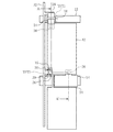
12…ゲートバスライン
14…補助容量バスライン
16…ゲート絶縁膜
18,20…アモルファスシリコン層
22…チャネル保護層
24,26…ソース電極
28,30…ドレイン電極
32…ドレインバスライン
34…補助容量電極
36,38…コンタクトホール
40…絶縁膜
42…画素電極
44,56…配向膜
52…カラーフィルタ
54…共通電極
60…液晶
70,76…パターン重畳部
72,74…パターンが重なっていない領域
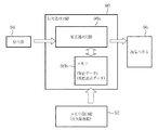
80…ゲートドライバ
82…データドライバ
84…補助容量バスライン用駆動回路
90…信号処理回路
90a…補正処理回路
90b…内部メモリ
92…メモリ
94…信号源
96…液晶パネル
Claims (6)
- 行方向及び列方向に隣接するようにマトリクス状に配置された複数の画素部と、前記行方向に延在し、前記行方向に並ぶ前記画素部に接続された複数のゲートバスラインと、前記列方向に延在し、前記列方向に並ぶ前記画素部に接続された複数のドレインバスラインと、前記行方向に延在し、前記行方向に並ぶ前記画素部に接続された補助容量バスラインとを有する液晶表示装置であって、
複数の前記画素部は、画素電極と、前記画素電極に接続され、前記補助容量バスラインとにより補助容量を構成する補助容量電極と、前記画素電極及び前記ドレインバスラインに接続され、前記画素電極と前記ドレインバスラインとの接続を前記ゲートバスラインにより制御する第1のスイッチング素子と、一方の電極が前記ドレインバスラインに接続され、他方の電極が前記画素電極に絶縁膜を介して重畳するように配置され、前記一方の電極と前記他方の電極との接続を前記補助容量バスラインにより制御する第2のスイッチング素子とをそれぞれ有し、
複数の前記画素部のうち少なくとも一の前記画素部は、前記第2のスイッチング素子の前記他方の電極が、前記絶縁膜を介して前記画素電極に重畳する部分において、前記画素電極に接続されている
ことを特徴とする液晶表示装置。 - 行方向及び列方向に隣接するようにマトリクス状に配置された複数の画素部と、前記行方向に延在し、前記行方向に並ぶ前記画素部に接続された複数のゲートバスラインと、前記列方向に延在し、前記列方向に並ぶ前記画素部に接続された複数のドレインバスラインと、前記行方向に延在し、前記行方向に並ぶ前記画素部に接続された補助容量バスラインとを有し、
複数の前記画素部が、画素電極と、前記画素電極に接続され、前記補助容量バスラインとにより補助容量を構成する補助容量電極と、前記画素電極及び前記ドレインバスラインに接続され、前記画素電極と前記ドレインバスラインとの接続を前記ゲートバスラインにより制御する第1のスイッチング素子と、一方の電極が前記ドレインバスラインに接続され、他方の電極が前記画素電極に絶縁膜を介して重畳するように配置され、前記一方の電極と前記他方の電極との接続を前記補助容量バスラインにより制御する第2のスイッチング素子とをそれぞれ有する液晶表示装置のリペア方法であって、
動作しない前記画素部が存在した場合、動作しない前記画素部の前記画素電極と前記第2のスイッチング素子の前記他方の電極との重畳部分にレーザ光を照射し、前記画素電極と前記第2のスイッチング素子の前記他方の電極とを接続する
ことを特徴とする液晶表示装置のリペア方法。 - 請求項2記載の液晶表示装置のリペア方法において、
レーザ光を照射することにより、前記補助容量電極と前記画素電極との間の接続を切断する
ことを特徴とする液晶表示装置のリペア方法。 - 請求項2又は3記載の液晶表示装置のリペア方法において、
レーザ光を照射することにより、前記第1のスイッチング素子と前記画素電極との間の接続を切断する
ことを特徴とする液晶表示装置のリペア方法。 - 行方向及び列方向に隣接するようにマトリクス状に配置された複数の画素部と、前記行方向に延在し、前記行方向に並ぶ前記画素部に接続された複数のゲートバスラインと、前記列方向に延在し、前記列方向に並ぶ前記画素部に接続された複数のドレインバスラインと、前記行方向に延在し、前記行方向に並ぶ前記画素部に接続された補助容量バスラインとを有し、
複数の前記画素部が、画素電極と、前記画素電極に接続され、前記補助容量バスラインとにより補助容量を構成する補助容量電極と、前記画素電極及び前記ドレインバスラインに接続され、前記画素電極と前記ドレインバスラインとの接続を前記ゲートバスラインにより制御する第1のスイッチング素子と、一方の電極が前記ドレインバスラインに接続され、他方の電極が前記画素電極に絶縁膜を介して重畳するように配置され、前記一方の電極と前記他方の電極との接続を前記補助容量バスラインにより制御する第2のスイッチング素子とをそれぞれ有し、
複数の前記画素部のうち正常に動作しない前記画素部では、レーザリペアによって、前記第2のスイッチング素子の前記他方の電極が、前記絶縁膜を介して前記画素電極に重畳する部分において、前記画素電極に接続されている液晶表示装置の駆動方法であって、
正常に動作する前記画素部では、前記ゲートバスラインにより前記第1のスイッチング素子を制御することにより、所定の画像情報を書き込み、
正常に動作しない前記画素部では、前記補助容量バスラインにより前記第2のスイッチング素子を制御することにより、所定の画像情報を書き込む
ことを特徴とする液晶表示装置の駆動方法。 - 請求項5記載の液晶表示装置の駆動方法において、
リペアした前記画素部の座標を記憶し、
記憶した前記座標に基づき、リペアした前記画素部に書き込むべきデータを記憶し、
複数の前記ゲートバスラインの総てが非選択の状態である期間に、リペアした前記画素部への前記データの書き込みを行う
ことを特徴とする液晶表示装置の駆動方法。
Priority Applications (2)
| Application Number | Priority Date | Filing Date | Title |
|---|---|---|---|
| JP2004211701A JP4498043B2 (ja) | 2004-07-20 | 2004-07-20 | 液晶表示装置、液晶表示装置のリペア方法及び液晶表示装置の駆動方法 |
| US11/063,081 US7978165B2 (en) | 2004-07-20 | 2005-02-22 | Liquid crystal display device, method for repairing liquid crystal display device, and method for driving liquid crystal display device |
Applications Claiming Priority (1)
| Application Number | Priority Date | Filing Date | Title |
|---|---|---|---|
| JP2004211701A JP4498043B2 (ja) | 2004-07-20 | 2004-07-20 | 液晶表示装置、液晶表示装置のリペア方法及び液晶表示装置の駆動方法 |
Publications (2)
| Publication Number | Publication Date |
|---|---|
| JP2006030782A JP2006030782A (ja) | 2006-02-02 |
| JP4498043B2 true JP4498043B2 (ja) | 2010-07-07 |
Family
ID=35656610
Family Applications (1)
| Application Number | Title | Priority Date | Filing Date |
|---|---|---|---|
| JP2004211701A Expired - Fee Related JP4498043B2 (ja) | 2004-07-20 | 2004-07-20 | 液晶表示装置、液晶表示装置のリペア方法及び液晶表示装置の駆動方法 |
Country Status (2)
| Country | Link |
|---|---|
| US (1) | US7978165B2 (ja) |
| JP (1) | JP4498043B2 (ja) |
Families Citing this family (14)
| Publication number | Priority date | Publication date | Assignee | Title |
|---|---|---|---|---|
| US10041176B2 (en) * | 2005-04-07 | 2018-08-07 | Momentive Performance Materials Inc. | No-rinse pretreatment methods and compositions |
| KR20070020778A (ko) * | 2005-08-17 | 2007-02-22 | 삼성전자주식회사 | 액정 표시 장치와 이의 검사 방법 및 이의 리페어 방법 |
| JP4633121B2 (ja) * | 2005-09-01 | 2011-02-16 | シャープ株式会社 | 表示装置ならびにその駆動回路および駆動方法 |
| JP2007298791A (ja) * | 2006-05-01 | 2007-11-15 | Mitsubishi Electric Corp | 液晶表示装置及びその欠陥修復方法 |
| US20080309532A1 (en) * | 2007-06-12 | 2008-12-18 | Silicon Optronics, Inc. | Solid-state imaging device and method of manufacturing thereof |
| CN104024933B (zh) * | 2011-10-31 | 2016-05-25 | 夏普株式会社 | 薄膜晶体管阵列基板和液晶显示装置 |
| JP5971849B2 (ja) * | 2012-07-11 | 2016-08-17 | パナソニック液晶ディスプレイ株式会社 | 表示装置及び画素欠陥修正方法 |
| CN103018987B (zh) * | 2012-12-06 | 2015-05-13 | 京东方科技集团股份有限公司 | 阵列基板及显示装置 |
| US9911799B2 (en) * | 2013-05-22 | 2018-03-06 | Samsung Display Co., Ltd. | Organic light-emitting display apparatus and method of repairing the same |
| CN104637450B (zh) * | 2015-03-13 | 2017-04-12 | 京东方科技集团股份有限公司 | 显示面板及其修复方法 |
| US10181284B2 (en) * | 2015-03-13 | 2019-01-15 | Boe Technology Group Co., Ltd. | Pixel driving circuit and repairing method thereof and display apparatus |
| CN110390900B (zh) * | 2018-04-19 | 2023-10-13 | 群创光电股份有限公司 | 显示器装置以及拼接式电子装置 |
| CN109102759B (zh) * | 2018-08-21 | 2019-11-22 | 友达光电股份有限公司 | 电子装置、显示面板与数据传输系统 |
| KR102921150B1 (ko) | 2022-12-30 | 2026-02-02 | 엘지디스플레이 주식회사 | 리페어 배선을 포함하는 디스플레이 장치 |
Family Cites Families (30)
| Publication number | Priority date | Publication date | Assignee | Title |
|---|---|---|---|---|
| JPS55129394A (en) * | 1979-03-29 | 1980-10-07 | Sony Corp | Xy matrix display unit |
| US4431271A (en) * | 1979-09-06 | 1984-02-14 | Canon Kabushiki Kaisha | Display device with a thin film transistor and storage condenser |
| JP3270112B2 (ja) * | 1992-06-17 | 2002-04-02 | 株式会社東芝 | 液晶表示素子 |
| EP0465111B1 (en) * | 1990-07-05 | 1996-05-15 | Matsushita Electric Industrial Co., Ltd. | Liquid crystal display device |
| JPH0450925A (ja) * | 1990-11-28 | 1992-02-19 | Seiko Epson Corp | 液晶表示装置 |
| JPH052184A (ja) * | 1991-06-26 | 1993-01-08 | Sanyo Electric Co Ltd | 液晶表示パネル |
| JP3150365B2 (ja) * | 1991-07-22 | 2001-03-26 | 株式会社東芝 | 液晶表示装置 |
| JPH0572553A (ja) * | 1991-09-11 | 1993-03-26 | Hitachi Ltd | 液晶表示装置およびその製造方法 |
| JP3102819B2 (ja) * | 1992-06-02 | 2000-10-23 | 富士通株式会社 | 液晶表示装置及びその駆動方法 |
| JP2860206B2 (ja) * | 1992-07-20 | 1999-02-24 | シャープ株式会社 | 液晶表示装置の駆動方法 |
| JP3332106B2 (ja) * | 1993-06-30 | 2002-10-07 | 株式会社東芝 | 液晶表示装置 |
| US5745090A (en) * | 1994-12-09 | 1998-04-28 | Samsung Electronics Co., Ltd. | Wiring structure and driving method for storage capacitors in a thin film transistor liquid crystal display device |
| JP3287985B2 (ja) | 1995-10-30 | 2002-06-04 | シャープ株式会社 | 液晶パネル及びその欠陥修正方法 |
| KR100286828B1 (ko) * | 1996-09-18 | 2001-04-16 | 니시무로 타이죠 | 플랫패널표시장치 |
| JPH10340070A (ja) * | 1997-06-09 | 1998-12-22 | Hitachi Ltd | 液晶表示装置 |
| JP3279238B2 (ja) * | 1997-12-01 | 2002-04-30 | 株式会社日立製作所 | 液晶表示装置 |
| US6066860A (en) * | 1997-12-25 | 2000-05-23 | Seiko Epson Corporation | Substrate for electro-optical apparatus, electro-optical apparatus, method for driving electro-optical apparatus, electronic device and projection display device |
| JPH11282007A (ja) | 1998-03-27 | 1999-10-15 | Toshiba Corp | 液晶表示装置 |
| JP3310615B2 (ja) | 1998-04-17 | 2002-08-05 | シャープ株式会社 | アクティブマトリクス型液晶表示装置および画素欠陥修正方法 |
| JP4517419B2 (ja) | 1999-08-18 | 2010-08-04 | ソニー株式会社 | 表示装置及びその修復方法 |
| JP4317624B2 (ja) * | 1999-09-10 | 2009-08-19 | メディア・テック・ユーエスエイ・インコーポレーテッド | 画像処理装置 |
| US6781659B2 (en) * | 2000-02-15 | 2004-08-24 | Matsushita Electric Industrial Co., Ltd. | Liquid crystal display device, pixels repair method thereof, and drive method thereof |
| JP2001305500A (ja) | 2000-04-19 | 2001-10-31 | Toshiba Corp | 液晶パネルのリペア方法 |
| KR100736114B1 (ko) * | 2000-05-23 | 2007-07-06 | 엘지.필립스 엘시디 주식회사 | 횡전계 방식의 액정표시장치 및 그 제조방법 |
| JP3520417B2 (ja) * | 2000-12-14 | 2004-04-19 | セイコーエプソン株式会社 | 電気光学パネルおよび電子機器 |
| JP4485087B2 (ja) * | 2001-03-01 | 2010-06-16 | 株式会社半導体エネルギー研究所 | 半導体装置の動作方法 |
| KR100796749B1 (ko) * | 2001-05-16 | 2008-01-22 | 삼성전자주식회사 | 액정 표시 장치용 박막 트랜지스터 어레이 기판 |
| JP4550334B2 (ja) * | 2001-09-27 | 2010-09-22 | 株式会社日立製作所 | 液晶表示装置および液晶表示装置の製造方法 |
| TWI228313B (en) * | 2003-11-21 | 2005-02-21 | Hannstar Display Corp | Pixel and repairing method thereof |
| JP2005173499A (ja) * | 2003-12-15 | 2005-06-30 | Sharp Corp | 液晶表示装置及びその製造方法 |
-
2004
- 2004-07-20 JP JP2004211701A patent/JP4498043B2/ja not_active Expired - Fee Related
-
2005
- 2005-02-22 US US11/063,081 patent/US7978165B2/en not_active Expired - Fee Related
Also Published As
| Publication number | Publication date |
|---|---|
| US7978165B2 (en) | 2011-07-12 |
| US20060017674A1 (en) | 2006-01-26 |
| JP2006030782A (ja) | 2006-02-02 |
Similar Documents
| Publication | Publication Date | Title |
|---|---|---|
| JP5335902B2 (ja) | 液晶パネル | |
| KR100769194B1 (ko) | 평판표시장치와 그 제조방법, 화질제어 방법 및 장치 | |
| US5289174A (en) | Liquid crystal display device | |
| CN107492357B (zh) | 有源矩阵基板、显示面板以及具备该显示面板的显示装置 | |
| US7612863B2 (en) | Liquid crystal display having a defect repair mechanism interposed between a light shielding storage line and a light shielding output electrode | |
| RU2479045C1 (ru) | Устройство отображения | |
| JP4498043B2 (ja) | 液晶表示装置、液晶表示装置のリペア方法及び液晶表示装置の駆動方法 | |
| EP2037444A1 (en) | Liquid crystal display | |
| JP2001188217A (ja) | アクティブマトリクス型液晶表示装置およびその駆動方法ならびに製造方法 | |
| JP5204314B2 (ja) | 液晶表示装置 | |
| US20120007843A1 (en) | Tft substrate and liquid crystal display apparatus using the same | |
| JP5238826B2 (ja) | 液晶表示装置 | |
| JP2008058337A (ja) | 表示装置、液晶表示装置、及び表示装置の製造方法 | |
| JP4393550B2 (ja) | アクティブマトリクス基板及びその画素欠陥修正方法 | |
| JP2005134882A (ja) | 液晶表示装置 | |
| US20100149155A1 (en) | Liquid crystal display device | |
| JP2009103810A (ja) | 液晶表示装置およびそのリペア方法 | |
| JP2022072553A (ja) | 液晶表示装置及びその駆動方法 | |
| WO2010032546A1 (ja) | 表示装置 | |
| KR20000001469U (ko) | 액정표시장치 | |
| JP2000206572A (ja) | アクティブマトリクス型液晶表示装置および画素欠陥修正方法 | |
| WO2017037953A1 (ja) | 液晶表示装置 |
Legal Events
| Date | Code | Title | Description |
|---|---|---|---|
| A621 | Written request for application examination |
Free format text: JAPANESE INTERMEDIATE CODE: A621 Effective date: 20060912 |
|
| A977 | Report on retrieval |
Free format text: JAPANESE INTERMEDIATE CODE: A971007 Effective date: 20090304 |
|
| A131 | Notification of reasons for refusal |
Free format text: JAPANESE INTERMEDIATE CODE: A131 Effective date: 20090421 |
|
| A521 | Request for written amendment filed |
Free format text: JAPANESE INTERMEDIATE CODE: A523 Effective date: 20090622 |
|
| A131 | Notification of reasons for refusal |
Free format text: JAPANESE INTERMEDIATE CODE: A131 Effective date: 20100105 |
|
| A521 | Request for written amendment filed |
Free format text: JAPANESE INTERMEDIATE CODE: A523 Effective date: 20100205 |
|
| TRDD | Decision of grant or rejection written | ||
| A01 | Written decision to grant a patent or to grant a registration (utility model) |
Free format text: JAPANESE INTERMEDIATE CODE: A01 Effective date: 20100413 |
|
| A01 | Written decision to grant a patent or to grant a registration (utility model) |
Free format text: JAPANESE INTERMEDIATE CODE: A01 |
|
| A61 | First payment of annual fees (during grant procedure) |
Free format text: JAPANESE INTERMEDIATE CODE: A61 Effective date: 20100413 |
|
| FPAY | Renewal fee payment (event date is renewal date of database) |
Free format text: PAYMENT UNTIL: 20130423 Year of fee payment: 3 |
|
| R150 | Certificate of patent or registration of utility model |
Free format text: JAPANESE INTERMEDIATE CODE: R150 |
|
| FPAY | Renewal fee payment (event date is renewal date of database) |
Free format text: PAYMENT UNTIL: 20130423 Year of fee payment: 3 |
|
| LAPS | Cancellation because of no payment of annual fees |