JP4503398B2 - 半導体パッケージ - Google Patents
半導体パッケージ Download PDFInfo
- Publication number
- JP4503398B2 JP4503398B2 JP2004248892A JP2004248892A JP4503398B2 JP 4503398 B2 JP4503398 B2 JP 4503398B2 JP 2004248892 A JP2004248892 A JP 2004248892A JP 2004248892 A JP2004248892 A JP 2004248892A JP 4503398 B2 JP4503398 B2 JP 4503398B2
- Authority
- JP
- Japan
- Prior art keywords
- seal ring
- brazing material
- metallized layer
- semiconductor package
- metal frame
- Prior art date
- Legal status (The legal status is an assumption and is not a legal conclusion. Google has not performed a legal analysis and makes no representation as to the accuracy of the status listed.)
- Expired - Fee Related
Links
Images


Classifications
-
- H—ELECTRICITY
- H10—SEMICONDUCTOR DEVICES; ELECTRIC SOLID-STATE DEVICES NOT OTHERWISE PROVIDED FOR
- H10W—GENERIC PACKAGES, INTERCONNECTIONS, CONNECTORS OR OTHER CONSTRUCTIONAL DETAILS OF DEVICES COVERED BY CLASS H10
- H10W90/00—Package configurations
- H10W90/701—Package configurations characterised by the relative positions of pads or connectors relative to package parts
- H10W90/751—Package configurations characterised by the relative positions of pads or connectors relative to package parts of bond wires
- H10W90/753—Package configurations characterised by the relative positions of pads or connectors relative to package parts of bond wires between laterally-adjacent chips
Landscapes
- Cooling Or The Like Of Semiconductors Or Solid State Devices (AREA)
Description
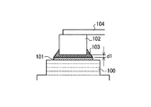
図1〜図3は参考例の半導体パッケージ1を示すものである。図1は半導体パッケージ1の全体構成を示すもので、図2は金属製シールリング近傍を拡大して示したもので、図3は金属製シールリングを表裏反転して示した図である。
図4および図5に従ってこの発明の実施の形態について説明する。この実施の形態においては、シールリング4とは別体であるスペーサ20を用いてシールリング4とメタライズ層11との間隔を確保するようにしている。
2 金属製ベース
3 誘電体多層基板
3a 凸状基台
4 シールリング
4a シールリング本体部
4b 突起
5 カバー(金属カバー)
6 IC搭載凹部
7 電子部品
8 接続材料
9,10 ろう材
11 メタライズ層
20 スペーサ
Claims (1)
- 半導体が実装される実装エリアの少なくとも周囲に金属枠体を取り付けるためのメタライズ層が形成された誘電体基板と、ろう材によって前記誘電体基板のメタライズ層上に接合される金属枠体と、該金属枠体上に配置される蓋体とを備える半導体パッケージにおいて、
前記金属枠体とメタライズ層との間に、間欠的に配置された複数のスペーサを介在させて前記ろう材による接合を行い、
前記スペーサは、前記金属枠体と別体の球形状を呈している
ことを特徴とする半導体パッケージ。
Priority Applications (1)
| Application Number | Priority Date | Filing Date | Title |
|---|---|---|---|
| JP2004248892A JP4503398B2 (ja) | 2004-08-27 | 2004-08-27 | 半導体パッケージ |
Applications Claiming Priority (1)
| Application Number | Priority Date | Filing Date | Title |
|---|---|---|---|
| JP2004248892A JP4503398B2 (ja) | 2004-08-27 | 2004-08-27 | 半導体パッケージ |
Publications (2)
| Publication Number | Publication Date |
|---|---|
| JP2006066721A JP2006066721A (ja) | 2006-03-09 |
| JP4503398B2 true JP4503398B2 (ja) | 2010-07-14 |
Family
ID=36112906
Family Applications (1)
| Application Number | Title | Priority Date | Filing Date |
|---|---|---|---|
| JP2004248892A Expired - Fee Related JP4503398B2 (ja) | 2004-08-27 | 2004-08-27 | 半導体パッケージ |
Country Status (1)
| Country | Link |
|---|---|
| JP (1) | JP4503398B2 (ja) |
Families Citing this family (1)
| Publication number | Priority date | Publication date | Assignee | Title |
|---|---|---|---|---|
| JP5515223B2 (ja) * | 2008-02-12 | 2014-06-11 | ソニー株式会社 | 半導体装置 |
Family Cites Families (4)
| Publication number | Priority date | Publication date | Assignee | Title |
|---|---|---|---|---|
| JPH0256447U (ja) * | 1988-10-14 | 1990-04-24 | ||
| JP2889519B2 (ja) * | 1995-11-13 | 1999-05-10 | 株式会社住友金属エレクトロデバイス | セラミックパッケージの封止構造 |
| JP2000263533A (ja) * | 1999-03-16 | 2000-09-26 | Sumitomo Metal Electronics Devices Inc | セラミック基板及びその製造方法 |
| JP3556567B2 (ja) * | 2000-04-27 | 2004-08-18 | 京セラ株式会社 | 電子部品収納用パッケージ |
-
2004
- 2004-08-27 JP JP2004248892A patent/JP4503398B2/ja not_active Expired - Fee Related
Also Published As
| Publication number | Publication date |
|---|---|
| JP2006066721A (ja) | 2006-03-09 |
Similar Documents
| Publication | Publication Date | Title |
|---|---|---|
| US5644163A (en) | Semiconductor device | |
| US5923083A (en) | Packaging technology for Schottky die | |
| JP4503398B2 (ja) | 半導体パッケージ | |
| JP2014175567A (ja) | セラミックパッケージ | |
| JP3878899B2 (ja) | 電子装置及びその製造方法 | |
| JP2006332599A (ja) | 電子装置 | |
| JP4614594B2 (ja) | 電子部品収納用パッケージ | |
| JP2004047897A (ja) | 電子部品および電子部品の製造方法 | |
| JP3377850B2 (ja) | 表面実装型水晶発振器及びその製造方法 | |
| JPWO2020045563A1 (ja) | 半導体パッケージおよびこれを備えた半導体装置 | |
| JP2006114601A (ja) | 蓋体と電子部品用パッケージ | |
| JP4284168B2 (ja) | 電子部品収納用パッケージおよび電子装置 | |
| JP2005244146A (ja) | 電子部品収納用パッケージおよび電子装置ならびに電子装置の実装構造 | |
| JPWO2019208577A1 (ja) | 放熱基板および電子装置 | |
| JP2001308211A (ja) | 電子部品収納用パッケージ | |
| JP4562301B2 (ja) | 電子部品収納用パッケージ | |
| JP2005101376A (ja) | 電子部品収納用パッケージおよび電子装置 | |
| JP2017126647A (ja) | 電子部品パッケージおよび電子モジュール | |
| JP2003110037A (ja) | 電子部品収納用パッケージ | |
| JP3847216B2 (ja) | 配線基板 | |
| JP4659653B2 (ja) | 電子部品収容パッケージおよび電子部品収容パッケージに用いられるシールリングの製造方法 | |
| JP2002170895A (ja) | 電子部品収納用パッケージおよびその封止方法 | |
| JP4214146B2 (ja) | 多数個取り配線基板上の小型配線基板の封止方法。 | |
| JP3780503B2 (ja) | 配線基板 | |
| JP4331957B2 (ja) | 圧電振動子収納用パッケージ |
Legal Events
| Date | Code | Title | Description |
|---|---|---|---|
| A621 | Written request for application examination |
Free format text: JAPANESE INTERMEDIATE CODE: A621 Effective date: 20070529 |
|
| A977 | Report on retrieval |
Free format text: JAPANESE INTERMEDIATE CODE: A971007 Effective date: 20090623 |
|
| A131 | Notification of reasons for refusal |
Free format text: JAPANESE INTERMEDIATE CODE: A131 Effective date: 20090630 |
|
| A521 | Request for written amendment filed |
Free format text: JAPANESE INTERMEDIATE CODE: A523 Effective date: 20090831 |
|
| A131 | Notification of reasons for refusal |
Free format text: JAPANESE INTERMEDIATE CODE: A131 Effective date: 20091006 |
|
| A521 | Request for written amendment filed |
Free format text: JAPANESE INTERMEDIATE CODE: A523 Effective date: 20091130 |
|
| A131 | Notification of reasons for refusal |
Free format text: JAPANESE INTERMEDIATE CODE: A131 Effective date: 20100105 |
|
| A521 | Request for written amendment filed |
Free format text: JAPANESE INTERMEDIATE CODE: A523 Effective date: 20100210 |
|
| TRDD | Decision of grant or rejection written | ||
| A01 | Written decision to grant a patent or to grant a registration (utility model) |
Free format text: JAPANESE INTERMEDIATE CODE: A01 Effective date: 20100420 |
|
| A01 | Written decision to grant a patent or to grant a registration (utility model) |
Free format text: JAPANESE INTERMEDIATE CODE: A01 |
|
| A61 | First payment of annual fees (during grant procedure) |
Free format text: JAPANESE INTERMEDIATE CODE: A61 Effective date: 20100421 |
|
| R150 | Certificate of patent or registration of utility model |
Free format text: JAPANESE INTERMEDIATE CODE: R150 |
|
| FPAY | Renewal fee payment (event date is renewal date of database) |
Free format text: PAYMENT UNTIL: 20130430 Year of fee payment: 3 |
|
| FPAY | Renewal fee payment (event date is renewal date of database) |
Free format text: PAYMENT UNTIL: 20130430 Year of fee payment: 3 |
|
| FPAY | Renewal fee payment (event date is renewal date of database) |
Free format text: PAYMENT UNTIL: 20140430 Year of fee payment: 4 |
|
| LAPS | Cancellation because of no payment of annual fees |