JP4594076B2 - 画像表示装置 - Google Patents
画像表示装置 Download PDFInfo
- Publication number
- JP4594076B2 JP4594076B2 JP2004377472A JP2004377472A JP4594076B2 JP 4594076 B2 JP4594076 B2 JP 4594076B2 JP 2004377472 A JP2004377472 A JP 2004377472A JP 2004377472 A JP2004377472 A JP 2004377472A JP 4594076 B2 JP4594076 B2 JP 4594076B2
- Authority
- JP
- Japan
- Prior art keywords
- layer
- spacer
- thin film
- divided
- metal back
- Prior art date
- Legal status (The legal status is an assumption and is not a legal conclusion. Google has not performed a legal analysis and makes no representation as to the accuracy of the status listed.)
- Expired - Fee Related
Links
Images


Classifications
-
- H—ELECTRICITY
- H01—ELECTRIC ELEMENTS
- H01J—ELECTRIC DISCHARGE TUBES OR DISCHARGE LAMPS
- H01J31/00—Cathode ray tubes; Electron beam tubes
- H01J31/08—Cathode ray tubes; Electron beam tubes having a screen on or from which an image or pattern is formed, picked up, converted, or stored
- H01J31/10—Image or pattern display tubes, i.e. having electrical input and optical output; Flying-spot tubes for scanning purposes
- H01J31/12—Image or pattern display tubes, i.e. having electrical input and optical output; Flying-spot tubes for scanning purposes with luminescent screen
- H01J31/123—Flat display tubes
- H01J31/125—Flat display tubes provided with control means permitting the electron beam to reach selected parts of the screen, e.g. digital selection
- H01J31/127—Flat display tubes provided with control means permitting the electron beam to reach selected parts of the screen, e.g. digital selection using large area or array sources, i.e. essentially a source for each pixel group
-
- H—ELECTRICITY
- H01—ELECTRIC ELEMENTS
- H01J—ELECTRIC DISCHARGE TUBES OR DISCHARGE LAMPS
- H01J29/00—Details of cathode-ray tubes or of electron-beam tubes of the types covered by group H01J31/00
- H01J29/86—Vessels; Containers; Vacuum locks
- H01J29/864—Spacers between faceplate and backplate of flat panel cathode ray tubes
-
- H—ELECTRICITY
- H01—ELECTRIC ELEMENTS
- H01J—ELECTRIC DISCHARGE TUBES OR DISCHARGE LAMPS
- H01J2329/00—Electron emission display panels, e.g. field emission display panels
- H01J2329/86—Vessels
- H01J2329/8625—Spacing members
Landscapes
- Cathode-Ray Tubes And Fluorescent Screens For Display (AREA)
- Vessels, Lead-In Wires, Accessory Apparatuses For Cathode-Ray Tubes (AREA)
Description
上記前面基板と対向して配置されているとともに、上記蛍光面に向けて電子を放出する複数の電子放出素子が配置された背面基板と、
前記前面基板および背面基板に作用する大気圧荷重を支持する複数のスペーサと、を備え、
前記第1方向に延在する分断部に形成された薄膜分断層上に、前記第1方向に離散的にスペーサ当接層が設けられていて、該スペーサ当接層にスペーサが当接されている一方、前記スペーサ当接層の前記第2方向両端部が、前記第1方向に延在する分断部に形成された薄膜分断層の前記第2方向両側に位置した分断メタルバック層に重なっている画像表示装置を提供するものである。
図1および図2に示すように、FEDは、それぞれ矩形状のガラス板からなる前面基板11、および背面基板12を備え、これらの基板は1〜2mmのギャップを置いて対向配置されている。前面基板11および背面基板122は、矩形枠状の側壁13を介して周縁部同士が接合され、内部が10−4Pa程度以下の高真空に維持された偏平な矩形状の真空外囲器10を構成している。側壁13は、例えば、低融点ガラス、低融点金属等の封着材23により、前面基板11の周縁部および背面基板12の周縁部に封着され、これらの基板同士を接合している。
図4ないし図6に示すように、遮光層17の上には、抵抗調整層30が形成されている。抵抗調整層30は、マトリックス部17bの領域においては、それぞれ第1方向Xに隣合う蛍光体層間を第2方向Yに延びた複数の第1抵抗調整層31Vと、それぞれ第2方向に隣合う蛍光体層間を第1方向Xに延びた複数の第2抵抗調整層31Hとを有している。蛍光体層は第1方向XにR、G、Bと並んでいるため、第1抵抗調整層31Vは、第2抵抗調整層31Hよりも幅が狭くなっている。例えば、第1抵抗調整層31Vの幅は40μm、第2抵抗調整層31Hの幅は300μmである。
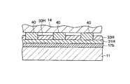
第2の実施形態によれば、各スペーサ14はスペーサ当接層40を介して第2抵抗調整層31Hに当接している。そのため、スペーサ14を介して薄膜分断層32に押圧力が作用することを防止し、薄膜分断層の損傷および剥離を一層確実に防止することができる。
各構成要素の寸法、材料等は、上述の実施の形態で示した数値、材料に限定されることなく、必要に応じて種々選択可能である。上述した実施形態において、複数のスペーサ当接層は、スペーサと対向する薄膜分断層の横線部のみに設ける構成としたが、これに限らず、全ての横線部にスペーサ当接層を設けても良い。更に、スペーサは板状に限らず、柱状のスペーサを用いても良い。
18…電子放出素子、 20…メタルバック層、 20a…分断メタルバック層、
22…遮光層、 30…抵抗調整層、 31V…第1抵抗調整層、
31H…第2抵抗調整層、 32…薄膜分断層、 40…スペーサ当接層、
Claims (5)
- 第1方向および第1方向と直交する第2方向にそれぞれ所定のピッチで並んで設けられた複数の蛍光体層および遮光層を含む蛍光面と、この蛍光面に重ねて設けられ、前記第1方向および第2方向に分断された分断メタルバック層と、この分断メタルバック層に重ねて設けられ、前記第1方向および第2方向に分断された分断ゲッター膜と、少なくとも前記分断メタルバックおよび分断ゲッターの第1方向および第2方向に延在する分断部に形成された薄膜分断層と、を有した前面基板と、
上記前面基板と対向して配置されているとともに、上記蛍光面に向けて電子を放出する複数の電子放出素子が配置された背面基板と、
前記前面基板および背面基板に作用する大気圧荷重を支持する複数のスペーサと、を備え、
前記第1方向に延在する分断部に形成された薄膜分断層上に、前記第1方向に離散的にスペーサ当接層が設けられていて、該スペーサ当接層にスペーサが当接されている一方、前記スペーサ当接層の前記第2方向両端部が、前記第1方向に延在する分断部に形成された薄膜分断層の前記第2方向両側に位置した分断メタルバック層に重なっている画像表示装置。 - 前記スペーサ当接層の上面が、前記薄膜分断層の上面より前記背面基板側に位置している請求項1に記載の画像表示装置。
- 前記スペーサ当接層の前記第2方向両端部は、前記第1方向に延在する分断部に形成された薄膜分断層の第2方向両側に2つずつ位置した4つの分断メタルバック層に重なって設けられている請求項1又は2に記載の画像表示装置。
- 前記スペーサ当接層は導電性を有している請求項1ないし3のいずれか1項に記載の画像表示装置。
- 前記各スペーサは細長い板状に形成され、前記第1方向に延びている請求項1ないし4のいずれか1項に記載の画像表示装置。
Priority Applications (5)
| Application Number | Priority Date | Filing Date | Title |
|---|---|---|---|
| JP2004377472A JP4594076B2 (ja) | 2004-12-27 | 2004-12-27 | 画像表示装置 |
| PCT/JP2005/023067 WO2006070613A1 (ja) | 2004-12-27 | 2005-12-15 | 画像表示装置 |
| EP05816512A EP1833074B1 (en) | 2004-12-27 | 2005-12-15 | Image display device |
| TW094145305A TW200632975A (en) | 2004-12-27 | 2005-12-20 | Image display device |
| US11/768,248 US7692370B2 (en) | 2004-12-27 | 2007-06-26 | Image display apparatus |
Applications Claiming Priority (1)
| Application Number | Priority Date | Filing Date | Title |
|---|---|---|---|
| JP2004377472A JP4594076B2 (ja) | 2004-12-27 | 2004-12-27 | 画像表示装置 |
Publications (2)
| Publication Number | Publication Date |
|---|---|
| JP2006185723A JP2006185723A (ja) | 2006-07-13 |
| JP4594076B2 true JP4594076B2 (ja) | 2010-12-08 |
Family
ID=36614733
Family Applications (1)
| Application Number | Title | Priority Date | Filing Date |
|---|---|---|---|
| JP2004377472A Expired - Fee Related JP4594076B2 (ja) | 2004-12-27 | 2004-12-27 | 画像表示装置 |
Country Status (5)
| Country | Link |
|---|---|
| US (1) | US7692370B2 (ja) |
| EP (1) | EP1833074B1 (ja) |
| JP (1) | JP4594076B2 (ja) |
| TW (1) | TW200632975A (ja) |
| WO (1) | WO2006070613A1 (ja) |
Families Citing this family (3)
| Publication number | Priority date | Publication date | Assignee | Title |
|---|---|---|---|---|
| JP4750413B2 (ja) * | 2004-12-27 | 2011-08-17 | キヤノン株式会社 | 画像表示装置 |
| US8350458B2 (en) | 2009-05-15 | 2013-01-08 | Canon Kabushiki Kaisha | Display panel and image display apparatus |
| JP2010267541A (ja) | 2009-05-15 | 2010-11-25 | Canon Inc | 表示パネル及び画像表示装置 |
Family Cites Families (13)
| Publication number | Priority date | Publication date | Assignee | Title |
|---|---|---|---|---|
| CN1271675C (zh) * | 1994-06-27 | 2006-08-23 | 佳能株式会社 | 电子束设备 |
| JPH10188863A (ja) * | 1996-12-27 | 1998-07-21 | Canon Inc | 画像表示装置 |
| JP3199682B2 (ja) | 1997-03-21 | 2001-08-20 | キヤノン株式会社 | 電子放出装置及びそれを用いた画像形成装置 |
| JP3234188B2 (ja) * | 1997-03-31 | 2001-12-04 | キヤノン株式会社 | 画像形成装置とその製造方法 |
| JP3466870B2 (ja) * | 1997-04-22 | 2003-11-17 | キヤノン株式会社 | 画像形成装置の製造方法 |
| JP2000251797A (ja) | 1999-02-25 | 2000-09-14 | Canon Inc | 画像形成装置 |
| JP4304809B2 (ja) | 1999-03-05 | 2009-07-29 | ソニー株式会社 | 表示用パネル及びこれを用いた表示装置 |
| JP2003068237A (ja) | 2001-08-24 | 2003-03-07 | Toshiba Corp | 画像表示装置およびその製造方法 |
| JP4036078B2 (ja) * | 2002-11-05 | 2008-01-23 | ソニー株式会社 | 冷陰極電界電子放出表示装置 |
| JP2004335346A (ja) * | 2003-05-09 | 2004-11-25 | Toshiba Corp | 画像表示装置 |
| US7138758B2 (en) | 2003-05-15 | 2006-11-21 | Canon Kabushiki Kaisha | Image forming apparatus having a high-resistance coated spacer in electrical contact with wirings components at predetermined intervals |
| JP3840233B2 (ja) * | 2003-05-15 | 2006-11-01 | キヤノン株式会社 | 画像形成装置 |
| JP2005123066A (ja) * | 2003-10-17 | 2005-05-12 | Toshiba Corp | 画像表示装置 |
-
2004
- 2004-12-27 JP JP2004377472A patent/JP4594076B2/ja not_active Expired - Fee Related
-
2005
- 2005-12-15 WO PCT/JP2005/023067 patent/WO2006070613A1/ja not_active Ceased
- 2005-12-15 EP EP05816512A patent/EP1833074B1/en not_active Expired - Lifetime
- 2005-12-20 TW TW094145305A patent/TW200632975A/zh not_active IP Right Cessation
-
2007
- 2007-06-26 US US11/768,248 patent/US7692370B2/en not_active Expired - Fee Related
Also Published As
| Publication number | Publication date |
|---|---|
| US7692370B2 (en) | 2010-04-06 |
| JP2006185723A (ja) | 2006-07-13 |
| EP1833074B1 (en) | 2012-02-15 |
| US20080122339A1 (en) | 2008-05-29 |
| TW200632975A (en) | 2006-09-16 |
| WO2006070613A1 (ja) | 2006-07-06 |
| TWI302328B (ja) | 2008-10-21 |
| EP1833074A4 (en) | 2010-06-16 |
| EP1833074A1 (en) | 2007-09-12 |
Similar Documents
| Publication | Publication Date | Title |
|---|---|---|
| JP3878365B2 (ja) | 画像表示装置および画像表示装置の製造方法 | |
| JP2006120622A (ja) | 発光スクリーン構造及び画像形成装置 | |
| JP2005011700A (ja) | 画像表示装置 | |
| JP4594076B2 (ja) | 画像表示装置 | |
| JP2008159449A (ja) | 表示装置 | |
| KR100761578B1 (ko) | 화상 표시 장치 | |
| JP4551755B2 (ja) | 画像表示装置 | |
| WO2003071576A1 (en) | Image display device | |
| JP2006004807A (ja) | 平面型表示装置 | |
| JP2005085728A (ja) | 画像表示装置 | |
| JP2006114403A (ja) | 画像表示装置 | |
| JP2005158498A (ja) | 平面表示装置 | |
| EP1768160A1 (en) | Image display device | |
| JPWO2005096398A1 (ja) | 画像表示装置 | |
| JP2006092963A (ja) | 画像表示装置 | |
| JP2006172890A (ja) | 画像表示装置 | |
| JP2006164919A (ja) | 画像表示装置 | |
| JP2006066201A (ja) | 画像表示装置およびその製造方法 | |
| JP2006093051A (ja) | 画像表示装置 | |
| JP2005294159A (ja) | 画像表示装置 | |
| JP2006019219A (ja) | 表示装置 | |
| JP2008166056A (ja) | 画像表示装置、及び画像表示装置の製造方法 | |
| JP2005209661A (ja) | 画像表示装置 | |
| JP2006059643A (ja) | 画像表示装置 | |
| JP2006318932A (ja) | カラー画像表示装置 |
Legal Events
| Date | Code | Title | Description |
|---|---|---|---|
| A621 | Written request for application examination |
Free format text: JAPANESE INTERMEDIATE CODE: A621 Effective date: 20071225 |
|
| A711 | Notification of change in applicant |
Free format text: JAPANESE INTERMEDIATE CODE: A711 Effective date: 20080619 |
|
| A131 | Notification of reasons for refusal |
Free format text: JAPANESE INTERMEDIATE CODE: A131 Effective date: 20100202 |
|
| A521 | Request for written amendment filed |
Free format text: JAPANESE INTERMEDIATE CODE: A523 Effective date: 20100325 |
|
| A131 | Notification of reasons for refusal |
Free format text: JAPANESE INTERMEDIATE CODE: A131 Effective date: 20100706 |
|
| A521 | Request for written amendment filed |
Free format text: JAPANESE INTERMEDIATE CODE: A523 Effective date: 20100729 |
|
| TRDD | Decision of grant or rejection written | ||
| A01 | Written decision to grant a patent or to grant a registration (utility model) |
Free format text: JAPANESE INTERMEDIATE CODE: A01 Effective date: 20100914 |
|
| A01 | Written decision to grant a patent or to grant a registration (utility model) |
Free format text: JAPANESE INTERMEDIATE CODE: A01 |
|
| A61 | First payment of annual fees (during grant procedure) |
Free format text: JAPANESE INTERMEDIATE CODE: A61 Effective date: 20100916 |
|
| FPAY | Renewal fee payment (event date is renewal date of database) |
Free format text: PAYMENT UNTIL: 20130924 Year of fee payment: 3 |
|
| R150 | Certificate of patent or registration of utility model |
Free format text: JAPANESE INTERMEDIATE CODE: R150 |
|
| LAPS | Cancellation because of no payment of annual fees |