JP4620962B2 - 集積回路装置の製造方法及び酸化バナジウム膜の形成方法 - Google Patents
集積回路装置の製造方法及び酸化バナジウム膜の形成方法 Download PDFInfo
- Publication number
- JP4620962B2 JP4620962B2 JP2004101108A JP2004101108A JP4620962B2 JP 4620962 B2 JP4620962 B2 JP 4620962B2 JP 2004101108 A JP2004101108 A JP 2004101108A JP 2004101108 A JP2004101108 A JP 2004101108A JP 4620962 B2 JP4620962 B2 JP 4620962B2
- Authority
- JP
- Japan
- Prior art keywords
- film
- forming
- vanadium oxide
- layer
- resist film
- Prior art date
- Legal status (The legal status is an assumption and is not a legal conclusion. Google has not performed a legal analysis and makes no representation as to the accuracy of the status listed.)
- Expired - Fee Related
Links
Images




Classifications
-
- H—ELECTRICITY
- H10—SEMICONDUCTOR DEVICES; ELECTRIC SOLID-STATE DEVICES NOT OTHERWISE PROVIDED FOR
- H10P—GENERIC PROCESSES OR APPARATUS FOR THE MANUFACTURE OR TREATMENT OF DEVICES COVERED BY CLASS H10
- H10P14/00—Formation of materials, e.g. in the shape of layers or pillars
- H10P14/60—Formation of materials, e.g. in the shape of layers or pillars of insulating materials
- H10P14/69—Inorganic materials
- H10P14/692—Inorganic materials composed of oxides, glassy oxides or oxide-based glasses
- H10P14/6938—Inorganic materials composed of oxides, glassy oxides or oxide-based glasses the material containing at least one metal element, e.g. metal oxides, metal oxynitrides or metal oxycarbides
- H10P14/6939—Inorganic materials composed of oxides, glassy oxides or oxide-based glasses the material containing at least one metal element, e.g. metal oxides, metal oxynitrides or metal oxycarbides characterised by the metal
- H10P14/69396—Inorganic materials composed of oxides, glassy oxides or oxide-based glasses the material containing at least one metal element, e.g. metal oxides, metal oxynitrides or metal oxycarbides characterised by the metal the material containing at least one rare earth metal element, e.g. oxides of lanthanides, scandium or yttrium
-
- H—ELECTRICITY
- H10—SEMICONDUCTOR DEVICES; ELECTRIC SOLID-STATE DEVICES NOT OTHERWISE PROVIDED FOR
- H10D—INORGANIC ELECTRIC SEMICONDUCTOR DEVICES
- H10D1/00—Resistors, capacitors or inductors
- H10D1/40—Resistors
- H10D1/47—Resistors having no potential barriers
- H10D1/474—Resistors having no potential barriers comprising refractory metals, transition metals, noble metals, metal compounds or metal alloys, e.g. silicides
-
- H—ELECTRICITY
- H10—SEMICONDUCTOR DEVICES; ELECTRIC SOLID-STATE DEVICES NOT OTHERWISE PROVIDED FOR
- H10N—ELECTRIC SOLID-STATE DEVICES NOT OTHERWISE PROVIDED FOR
- H10N15/00—Thermoelectric devices without a junction of dissimilar materials; Thermomagnetic devices, e.g. using the Nernst-Ettingshausen effect
-
- H—ELECTRICITY
- H10—SEMICONDUCTOR DEVICES; ELECTRIC SOLID-STATE DEVICES NOT OTHERWISE PROVIDED FOR
- H10P—GENERIC PROCESSES OR APPARATUS FOR THE MANUFACTURE OR TREATMENT OF DEVICES COVERED BY CLASS H10
- H10P14/00—Formation of materials, e.g. in the shape of layers or pillars
- H10P14/60—Formation of materials, e.g. in the shape of layers or pillars of insulating materials
- H10P14/66—Formation of materials, e.g. in the shape of layers or pillars of insulating materials characterised by the type of materials
- H10P14/662—Laminate layers, e.g. stacks of alternating high-k metal oxides
-
- H—ELECTRICITY
- H10—SEMICONDUCTOR DEVICES; ELECTRIC SOLID-STATE DEVICES NOT OTHERWISE PROVIDED FOR
- H10W—GENERIC PACKAGES, INTERCONNECTIONS, CONNECTORS OR OTHER CONSTRUCTIONAL DETAILS OF DEVICES COVERED BY CLASS H10
- H10W20/00—Interconnections in chips, wafers or substrates
- H10W20/40—Interconnections external to wafers or substrates, e.g. back-end-of-line [BEOL] metallisations or vias connecting to gate electrodes
- H10W20/498—Resistive arrangements or effects of, or between, wiring layers
Landscapes
- Semiconductor Integrated Circuits (AREA)
- Internal Circuitry In Semiconductor Integrated Circuit Devices (AREA)
- Drying Of Semiconductors (AREA)
Description
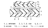
更に、層間絶縁膜4上には、抵抗体膜9、シリコン酸化膜13及びシリコン窒化膜14を埋め込むように、絶縁膜(図示せず)が設けられている。抵抗体膜9は、例えばこの集積回路装置における多層配線層の最上層に配置されている。
2、3、7、8;配線
5、6;ビア
9;抵抗体膜
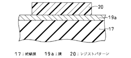
9a、19a;膜
13、13a、22;シリコン酸化膜
14、14a;シリコン窒化膜
15;アルミニウム膜
16、20;レジストパターン
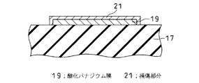
17;絶縁膜
19;酸化バナジウム膜
21;損傷部分
Claims (14)
- 基板上に、その表面に2本の配線が露出した絶縁膜を形成する工程と、この絶縁膜上における前記2本の配線の露出部を含む領域に酸化バナジウムを含む膜を形成する工程と、この膜上に酸化バナジウムとは異なる第1の材料からなる第1層を形成する工程と、この第1層上に酸化バナジウム及び前記第1の材料とは異なる第2の材料からなる第2層を形成する工程と、この第2層上にレジスト膜を形成する工程と、前記2本の配線の露出部及びこの露出部間を接続する領域の直上域を含む領域に前記レジスト膜が残留するように前記レジスト膜をパターニングする工程と、前記パターニングされたレジスト膜をマスクとして前記第2層をエッチングして選択的に除去しパターニングする工程と、前記パターニングされたレジスト膜を除去する工程と、前記パターニングされた第2層をマスクとして前記第1層及び前記酸化バナジウムを含む膜をエッチングして選択的に除去する工程と、を有することを特徴とする集積回路装置の製造方法。
- 前記レジスト膜を除去する工程は、前記レジスト膜を剥離液に溶解させる工程を有することを特徴とする請求項1に記載の集積回路装置の製造方法。
- 前記レジスト膜を除去する工程は、前記レジスト膜に対して酸素プラズマアッシングを行う工程を有することを特徴とする請求項1に記載の集積回路装置の製造方法。
- 前記第1層を形成する工程において、前記第1の材料を、シリコンを含む絶縁材料とすることを特徴とする請求項1乃至3のいずれか1項に記載の集積回路装置の製造方法。
- 前記第2層を形成する工程において、前記第2の材料を、シリコンを含む絶縁材料とすることを特徴とする請求項1乃至4のいずれか1項に記載の集積回路装置の製造方法。
- 前記第2層を形成する工程において、前記第2の材料を、金属又は合金とすることを特徴とする請求項1乃至4のいずれか1項に記載の集積回路装置の製造方法。
- 前記第2の材料を、Al、Ti、Cu、Ta、W及びNiからなる群から選択された1種の金属若しくはその合金又は2種以上の金属を含む合金とすることを特徴とする請求項6に記載の集積回路装置の製造方法。
- 基板上に酸化バナジウムを含む膜を成膜する工程と、この膜上に酸化バナジウムとは異なる第1の材料からなる第1層を形成する工程と、この第1層上に酸化バナジウム及び前記第1の材料とは異なる第2の材料からなる第2層を形成する工程と、この第2層上にレジスト膜を形成する工程と、前記レジスト膜をパターニングする工程と、前記パターニングされたレジスト膜をマスクとして前記第2層をエッチングして選択的に除去しパターニングする工程と、前記パターニングされたレジスト膜を除去する工程と、前記パターニングされた第2層をマスクとして前記第1層及び前記膜をエッチングして選択的に除去する工程と、を有することを特徴とする酸化バナジウム膜の形成方法。
- 前記レジスト膜を除去する工程は、前記レジスト膜を剥離液に溶解させる工程を有することを特徴とする請求項8に記載の酸化バナジウム膜の形成方法。
- 前記レジスト膜を除去する工程は、前記レジスト膜に対して酸素プラズマアッシングを行う工程を有することを特徴とする請求項8に記載の酸化バナジウム膜の形成方法。
- 前記第1層を形成する工程において、前記第1の材料を、シリコンを含む絶縁材料とすることを特徴とする請求項8乃至10のいずれか1項に記載の酸化バナジウム膜の形成方法。
- 前記第2層を形成する工程において、前記第2の材料を、シリコンを含む絶縁材料とすることを特徴とする請求項8乃至11のいずれか1項に記載の酸化バナジウム膜の形成方法。
- 前記第2層を形成する工程において、前記第2の材料を、金属又は合金とすることを特徴とする請求項8乃至11のいずれか1項に記載の酸化バナジウム膜の形成方法。
- 前記第2の材料を、Al、Ti、Cu、Ta、W及びNiからなる群から選択された1種の金属若しくはその合金又は2種以上の金属を含む合金とすることを特徴とする請求項13に記載の酸化バナジウム膜の形成方法。
Priority Applications (3)
| Application Number | Priority Date | Filing Date | Title |
|---|---|---|---|
| JP2004101108A JP4620962B2 (ja) | 2004-03-30 | 2004-03-30 | 集積回路装置の製造方法及び酸化バナジウム膜の形成方法 |
| US11/086,743 US7462921B2 (en) | 2004-03-30 | 2005-03-23 | Integrated circuit device, method of manufacturing the same and method of forming vanadium oxide film |
| CNB2005100625193A CN100490149C (zh) | 2004-03-30 | 2005-03-30 | 集成电路器件及其制造方法以及形成钒氧化物膜的方法 |
Applications Claiming Priority (1)
| Application Number | Priority Date | Filing Date | Title |
|---|---|---|---|
| JP2004101108A JP4620962B2 (ja) | 2004-03-30 | 2004-03-30 | 集積回路装置の製造方法及び酸化バナジウム膜の形成方法 |
Publications (2)
| Publication Number | Publication Date |
|---|---|
| JP2005286239A JP2005286239A (ja) | 2005-10-13 |
| JP4620962B2 true JP4620962B2 (ja) | 2011-01-26 |
Family
ID=35050074
Family Applications (1)
| Application Number | Title | Priority Date | Filing Date |
|---|---|---|---|
| JP2004101108A Expired - Fee Related JP4620962B2 (ja) | 2004-03-30 | 2004-03-30 | 集積回路装置の製造方法及び酸化バナジウム膜の形成方法 |
Country Status (3)
| Country | Link |
|---|---|
| US (1) | US7462921B2 (ja) |
| JP (1) | JP4620962B2 (ja) |
| CN (1) | CN100490149C (ja) |
Families Citing this family (4)
| Publication number | Priority date | Publication date | Assignee | Title |
|---|---|---|---|---|
| JP3810411B2 (ja) * | 2004-01-23 | 2006-08-16 | Necエレクトロニクス株式会社 | 集積回路装置 |
| JP4541717B2 (ja) * | 2004-02-09 | 2010-09-08 | ルネサスエレクトロニクス株式会社 | 集積回路装置及びその製造方法 |
| JP5567087B2 (ja) * | 2012-09-20 | 2014-08-06 | 株式会社東芝 | 半導体装置の製造方法 |
| US12372417B2 (en) * | 2022-07-01 | 2025-07-29 | International Business Machines Corporation | Adjustable transition edge thermometer |
Family Cites Families (5)
| Publication number | Priority date | Publication date | Assignee | Title |
|---|---|---|---|---|
| JPH01302849A (ja) | 1988-05-31 | 1989-12-06 | Fujitsu Ltd | 半導体集積回路装置 |
| JP3061012B2 (ja) * | 1997-08-27 | 2000-07-10 | 日本電気株式会社 | マイクロブリッジ構造及びその製造方法 |
| JP3067737B2 (ja) | 1998-05-18 | 2000-07-24 | 日本電気株式会社 | 酸化バナジウム膜のプラズマエッチング方法 |
| JP2002048636A (ja) * | 2000-08-03 | 2002-02-15 | Sharp Corp | 赤外線センサ |
| JP4135857B2 (ja) * | 2001-03-27 | 2008-08-20 | 独立行政法人産業技術総合研究所 | 赤外線センサの製造方法 |
-
2004
- 2004-03-30 JP JP2004101108A patent/JP4620962B2/ja not_active Expired - Fee Related
-
2005
- 2005-03-23 US US11/086,743 patent/US7462921B2/en active Active - Reinstated
- 2005-03-30 CN CNB2005100625193A patent/CN100490149C/zh not_active Expired - Fee Related
Also Published As
| Publication number | Publication date |
|---|---|
| CN100490149C (zh) | 2009-05-20 |
| JP2005286239A (ja) | 2005-10-13 |
| US20050221573A1 (en) | 2005-10-06 |
| CN1677670A (zh) | 2005-10-05 |
| US7462921B2 (en) | 2008-12-09 |
Similar Documents
| Publication | Publication Date | Title |
|---|---|---|
| US6703666B1 (en) | Thin film resistor device and a method of manufacture therefor | |
| JP4446771B2 (ja) | 半導体装置 | |
| US9679844B2 (en) | Manufacturing a damascene thin-film resistor | |
| CN107452714B (zh) | 形成低电阻率贵金属互连的装置及方法 | |
| US6211032B1 (en) | Method for forming silicon carbide chrome thin-film resistor | |
| CA2858087C (en) | Low temperature resistor for superconductor circuits | |
| JP3918612B2 (ja) | 磁気トンネル接合素子の製法と磁気トンネル接合装置 | |
| JP4620962B2 (ja) | 集積回路装置の製造方法及び酸化バナジウム膜の形成方法 | |
| CN110337710B (zh) | 用于铂图案化的牺牲层 | |
| US8551854B2 (en) | Method of manufacturing a semiconductor device | |
| JP2005235888A (ja) | 半導体装置及びその製造方法 | |
| US10211278B2 (en) | Device and method for a thin film resistor using a via retardation layer | |
| JP2001291706A (ja) | 高融点金属の加工方法及びこの金属を用いた半導体装置の製造方法 | |
| JP2003218431A (ja) | 磁気トンネル接合素子の製法 | |
| JP4534058B2 (ja) | 半導体製造方法および半導体装置 | |
| JPS61214538A (ja) | 配線構造体の製造方法 | |
| JP4363061B2 (ja) | 抵抗体を備えた半導体装置の製造方法 | |
| JPH11238732A (ja) | 配線構造およびボンディングパッド開口の形成法 | |
| JP5596403B2 (ja) | 半導体装置の製造方法 | |
| JPH08186120A (ja) | 半導体装置の製造方法 | |
| EP1203400A1 (en) | A thin film resistor device and a method of manufacture therefor | |
| KR100854209B1 (ko) | 반도체 장치 제조 방법 | |
| JP3877461B2 (ja) | 半導体装置の製造方法 | |
| JP3614771B2 (ja) | 半導体装置の製造方法 | |
| JP2013026388A (ja) | 導電膜パターンの形成方法 |
Legal Events
| Date | Code | Title | Description |
|---|---|---|---|
| A621 | Written request for application examination |
Free format text: JAPANESE INTERMEDIATE CODE: A621 Effective date: 20061208 |
|
| RD02 | Notification of acceptance of power of attorney |
Free format text: JAPANESE INTERMEDIATE CODE: A7422 Effective date: 20070112 |
|
| RD04 | Notification of resignation of power of attorney |
Free format text: JAPANESE INTERMEDIATE CODE: A7424 Effective date: 20080620 |
|
| A977 | Report on retrieval |
Free format text: JAPANESE INTERMEDIATE CODE: A971007 Effective date: 20100330 |
|
| A131 | Notification of reasons for refusal |
Free format text: JAPANESE INTERMEDIATE CODE: A131 Effective date: 20100406 |
|
| A521 | Request for written amendment filed |
Free format text: JAPANESE INTERMEDIATE CODE: A523 Effective date: 20100603 |
|
| A02 | Decision of refusal |
Free format text: JAPANESE INTERMEDIATE CODE: A02 Effective date: 20100622 |
|
| A521 | Request for written amendment filed |
Free format text: JAPANESE INTERMEDIATE CODE: A523 Effective date: 20100917 |
|
| A911 | Transfer to examiner for re-examination before appeal (zenchi) |
Free format text: JAPANESE INTERMEDIATE CODE: A911 Effective date: 20100929 |
|
| TRDD | Decision of grant or rejection written | ||
| A01 | Written decision to grant a patent or to grant a registration (utility model) |
Free format text: JAPANESE INTERMEDIATE CODE: A01 Effective date: 20101026 |
|
| A01 | Written decision to grant a patent or to grant a registration (utility model) |
Free format text: JAPANESE INTERMEDIATE CODE: A01 |
|
| A61 | First payment of annual fees (during grant procedure) |
Free format text: JAPANESE INTERMEDIATE CODE: A61 Effective date: 20101029 |
|
| FPAY | Renewal fee payment (event date is renewal date of database) |
Free format text: PAYMENT UNTIL: 20131105 Year of fee payment: 3 |
|
| R150 | Certificate of patent or registration of utility model |
Free format text: JAPANESE INTERMEDIATE CODE: R150 |
|
| R250 | Receipt of annual fees |
Free format text: JAPANESE INTERMEDIATE CODE: R250 |
|
| LAPS | Cancellation because of no payment of annual fees |