JP4649155B2 - 撮像装置及び撮像方法 - Google Patents
撮像装置及び撮像方法 Download PDFInfo
- Publication number
- JP4649155B2 JP4649155B2 JP2004275652A JP2004275652A JP4649155B2 JP 4649155 B2 JP4649155 B2 JP 4649155B2 JP 2004275652 A JP2004275652 A JP 2004275652A JP 2004275652 A JP2004275652 A JP 2004275652A JP 4649155 B2 JP4649155 B2 JP 4649155B2
- Authority
- JP
- Japan
- Prior art keywords
- level
- blanking
- optical black
- black level
- signal
- Prior art date
- Legal status (The legal status is an assumption and is not a legal conclusion. Google has not performed a legal analysis and makes no representation as to the accuracy of the status listed.)
- Expired - Fee Related
Links
Images


Classifications
-
- H—ELECTRICITY
- H04—ELECTRIC COMMUNICATION TECHNIQUE
- H04N—PICTORIAL COMMUNICATION, e.g. TELEVISION
- H04N25/00—Circuitry of solid-state image sensors [SSIS]; Control thereof
- H04N25/60—Noise processing, e.g. detecting, correcting, reducing or removing noise
- H04N25/62—Detection or reduction of noise due to excess charges produced by the exposure, e.g. smear, blooming, ghost image, crosstalk or leakage between pixels
- H04N25/621—Detection or reduction of noise due to excess charges produced by the exposure, e.g. smear, blooming, ghost image, crosstalk or leakage between pixels for the control of blooming
-
- H—ELECTRICITY
- H04—ELECTRIC COMMUNICATION TECHNIQUE
- H04N—PICTORIAL COMMUNICATION, e.g. TELEVISION
- H04N25/00—Circuitry of solid-state image sensors [SSIS]; Control thereof
- H04N25/60—Noise processing, e.g. detecting, correcting, reducing or removing noise
- H04N25/616—Noise processing, e.g. detecting, correcting, reducing or removing noise involving a correlated sampling function, e.g. correlated double sampling [CDS] or triple sampling
-
- H—ELECTRICITY
- H04—ELECTRIC COMMUNICATION TECHNIQUE
- H04N—PICTORIAL COMMUNICATION, e.g. TELEVISION
- H04N25/00—Circuitry of solid-state image sensors [SSIS]; Control thereof
- H04N25/60—Noise processing, e.g. detecting, correcting, reducing or removing noise
- H04N25/67—Noise processing, e.g. detecting, correcting, reducing or removing noise applied to fixed-pattern noise, e.g. non-uniformity of response
- H04N25/671—Noise processing, e.g. detecting, correcting, reducing or removing noise applied to fixed-pattern noise, e.g. non-uniformity of response for non-uniformity detection or correction
- H04N25/677—Noise processing, e.g. detecting, correcting, reducing or removing noise applied to fixed-pattern noise, e.g. non-uniformity of response for non-uniformity detection or correction for reducing the column or line fixed pattern noise
-
- H—ELECTRICITY
- H04—ELECTRIC COMMUNICATION TECHNIQUE
- H04N—PICTORIAL COMMUNICATION, e.g. TELEVISION
- H04N25/00—Circuitry of solid-state image sensors [SSIS]; Control thereof
- H04N25/60—Noise processing, e.g. detecting, correcting, reducing or removing noise
- H04N25/63—Noise processing, e.g. detecting, correcting, reducing or removing noise applied to dark current
- H04N25/633—Noise processing, e.g. detecting, correcting, reducing or removing noise applied to dark current by using optical black pixels
Landscapes
- Engineering & Computer Science (AREA)
- Multimedia (AREA)
- Signal Processing (AREA)
- Transforming Light Signals Into Electric Signals (AREA)
- Picture Signal Circuits (AREA)
- Studio Devices (AREA)
Description
また、本発明の撮像方法は、被写体の光学像を電気信号に変換する光電変換ステップと、前記光電変換ステップによる光電変換後の撮像信号に含まれる光学的黒レベルを抽出する光学的黒レベル抽出ステップと、前記撮像信号のブランキング期間におけるブランキングレベルを抽出するブランキングレベル抽出ステップと、前記抽出された光学的黒レベルを基準として第1の目標値にクランプする第1のモードと、前記抽出されたブランキングレベルを基準として第2の目標値にクランプする第2のモードとを備えるクランプステップと、前記光学的黒レベル抽出ステップで抽出した光学的黒レベルと、前記ブランキングレベル抽出ステップで抽出したブランキングレベルとの差が閾値より小さい場合には前記クランプステップにおいて第1のモードに設定し、当該差が前記閾値より大きい場合に前記クランプステップにおいて第2のモードに設定する制御ステップとを有することを特徴とする。
(第1の実施形態)
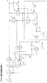
図1は、本発明の第1の実施形態によるフィードバック方式のOBクランプ回路の構成例を示すブロック図である。
積分アンプ6は、コンデンサ6B、抵抗6Cとにより所定の積分時定数を成しており、前記サンプルホールドされたOBレベルと、信号線7より入力される所定の基準電圧VREFとの差分電圧(クランプ誤差電圧)が前記積分時定数にて積分されるとともに、その出力(電圧VREFからのずれ量)が、減算値としてオフセット加算回路3に入力されて減算されるフィードバック制御の構成になっている。
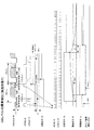
図2は、本実施形態におけるブルーミング発生時のクランプ動作を説明するための各部の動作波形を示したものである。
ところで、前記第1の実施形態で示したフィードバック方式のOBクランプ回路は、可変増幅器の出力信号をフィードバックする構成のものであったが、昨今の撮像機器のデジタル化に際して、可変増幅器の後段にA/D変換器を設けて、そのデジタル出力をフィードバックする構成も、一般に、よく利用されている。
図4の構成について説明すると、40は被写体の光学像を電気信号に変換するCCD(CCDイメージセンサ)であり、このCDD40から出力される撮像信号が、CDS(相関2重サンプリング)回路41に入力されてリセットノイズが除去された後に、オフセット加算回路43に入力されて所定のオフセット電圧が加算されて、そのオフセット加算出力が可変増幅器45に入力される。
ブルーミング発生時のクランプ動作を説明するための各部の動作波形であるが、本発明の第1の実施形態の説明で用いた図2の様子とほぼ同様であるので、図2を用いて(差異の部分を含めて)以下に説明する。
2 CDS回路
3、21 オフセット加算回路
4 可変増幅器
5 基準電圧VREF
6 積分増幅器
12、14 比較器
10、18 セレクタ
8 基準電圧VREF1
9 基準電圧VREF2
17、19、20 サンプルホールド回路
23 OBクランプパルス
24 ブランキングパルス
26 画像処理・記録・表示回路
40 CCD
41 CDS回路
42 基準電圧VREF
43 オフセット加算回路
44 バッファ回路
45 可変増幅器
48 コンデンサ
46 A/D変換器
49 電流DAC(D/A変換器)
60 画像処理・記録・表示回路
52 デジタル演算回路
47、56 データセレクタ
50 OBクランプパルス
57 ブランキングパルス
61 黒レベル異常検出回路
58 黒レベル目標値1
59 黒レベル目標値2
Claims (15)
- 被写体の光学像を電気信号に変換する撮像素子と、
前記撮像素子による光電変換後の撮像信号に含まれる光学的黒レベルを抽出する光学的黒レベル抽出手段と、
前記撮像信号のブランキング期間におけるブランキングレベルを抽出するブランキングレベル抽出手段と、
前記光学的黒レベル抽出手段により抽出された光学的黒レベルを基準として第1の目標値にクランプする第1のモードと、前記ブランキングレベル抽出手段により抽出されたブランキングレベルを基準として第2の目標値にクランプする第2のモードとを備えるクランプ手段と、
前記光学的黒レベル抽出手段で抽出した光学的黒レベルと、前記ブランキングレベル抽出手段で抽出したブランキングレベルとの差が閾値より小さい場合には前記クランプ手段を第1のモードに設定し、当該差が前記閾値より大きい場合に前記クランプ手段を第2のモードに設定する制御手段と
を有することを特徴とする撮像装置。 - さらに、前記撮像素子による光電変換後のアナログ撮像信号をデジタル撮像信号に変換するA/D変換手段を有し、
前記光学的黒レベル抽出手段及び前記ブランキングレベル抽出手段は、デジタル撮像信号に含まれる光学的黒レベル及びブランキングレベルを抽出し、
前記クランプ手段は、前記第1のモードでは前記光学的黒レベルを第1の目標値にクランプし、前記第2のモードでは前記ブランキングレベルを第2の目標値にクランプすることを特徴とする請求項1記載の撮像装置。 - 前記第1及び第2の目標値は、前記A/D変換手段のデジタル下限値に対応するボトム電圧と、前記光学的黒レベル抽出手段により抽出された光学的黒レベルと前記ブランキングレベル抽出手段により抽出されたブランキングレベルとのレベル差とに基づいて設定されることを特徴とする請求項2記載の撮像装置。
- 前記光学的黒レベル抽出手段及び前記ブランキングレベル抽出手段は、アナログ撮像信号をサンプルホールドするサンプルホールド手段である請求項1記載の撮像装置。
- 前記第2の目標値は、前記光学的黒レベル抽出手段により抽出された光学的黒レベルと前記ブランキングレベル抽出手段により抽出されたブランキングレベルとのレベル差に基づいて設定されることを特徴とする請求項4記載の撮像装置。
- 前記クランプ手段は、
前記撮像素子による光電変換後の電気信号に対して所定の直流電圧を加算するオフセット加算手段と、
前記第1のモードでは前記光学的黒レベル抽出手段により抽出された光学的黒レベルと第1の目標値との誤差信号を検出し、前記第2のモードでは前記ブランキングレベル抽出手段により抽出されたブランキングレベルと第2の目標値との誤差信号を検出する誤差信号検出手段とを有し、
前記光学的黒レベル抽出手段及び前記ブランキングレベル抽出手段は、前記オフセット加算手段による直流電圧加算処理後の撮像信号に含まれる光学的黒レベル及びブランキングレベルを抽出し、
前記検出された誤差信号を前記オフセット加算手段により前記撮像素子による光電変換後の電気信号から減算するための負帰還信号となすことで前記撮像信号の光学的黒レベルを所定の電圧にクランプすることを特徴とする請求項1記載の撮像装置。 - さらに、前記オフセット加算手段による直流電圧加算処理後のアナログ撮像信号をデジタル撮像信号に変換するA/D変換手段を有し、
前記光学的黒レベル抽出手段及び前記ブランキングレベル抽出手段は、デジタル撮像信号に含まれる光学的黒レベル及びブランキングレベルを抽出することを特徴とする請求項6記載の撮像装置。 - 前記第1及び第2の目標値は、前記A/D変換手段のデジタル下限値に対応するボトム電圧と、前記光学的黒レベル抽出手段により抽出された光学的黒レベルと前記ブランキングレベル抽出手段により抽出されたブランキングレベルとのレベル差とに基づいて設定されることを特徴とする請求項7記載の撮像装置。
- 前記光学的黒レベル抽出手段及び前記ブランキングレベル抽出手段は、アナログ撮像信号をサンプルホールドするサンプルホールド手段である請求項6記載の撮像装置。
- 前記第2の目標値は、前記光学的黒レベル抽出手段により抽出された光学的黒レベルと前記ブランキングレベル抽出手段により抽出されたブランキングレベルとのレベル差に基づいて設定されることを特徴とする請求項9記載の撮像装置。
- 前記ブランキング期間は、前記撮像素子からの画素信号の読み出しを停止している期間であることを特徴とする請求項1〜10のいずれか1項に記載の撮像装置。
- 前記誤差信号検出手段は、前記第1のモードでは前記撮像信号に含まれる光学的黒レベルの変動に対して、所定の積分時定数を持って誤差の検出を行うことを特徴とする請求項6記載の撮像装置。
- 前記制御手段は、前記撮像素子のばらつき及び温度特性による光学的黒レベルの変動量に応じて前記第1のモード又は前記第2のモードに設定することを特徴とする請求項1〜12のいずれか1項に記載の撮像装置。
- さらに、所定ゲイン又は可変ゲインで前記撮像信号を増幅するための増幅手段を有し、
前記第2の目標値は、前記増幅手段の増幅度に応じて設定されることを特徴とする請求項1〜13のいずれか1項に記載の撮像装置。 - 被写体の光学像を電気信号に変換する光電変換ステップと、
前記光電変換ステップによる光電変換後の撮像信号に含まれる光学的黒レベルを抽出する光学的黒レベル抽出ステップと、
前記撮像信号のブランキング期間におけるブランキングレベルを抽出するブランキングレベル抽出ステップと、
前記抽出された光学的黒レベルを基準として第1の目標値にクランプする第1のモードと、前記抽出されたブランキングレベルを基準として第2の目標値にクランプする第2のモードとを備えるクランプステップと、
前記光学的黒レベル抽出ステップで抽出した光学的黒レベルと、前記ブランキングレベル抽出ステップで抽出したブランキングレベルとの差が閾値より小さい場合には前記クランプステップにおいて第1のモードに設定し、当該差が前記閾値より大きい場合に前記クランプステップにおいて第2のモードに設定する制御ステップとを有することを特徴とする撮像方法。
Priority Applications (2)
| Application Number | Priority Date | Filing Date | Title |
|---|---|---|---|
| JP2004275652A JP4649155B2 (ja) | 2004-09-22 | 2004-09-22 | 撮像装置及び撮像方法 |
| US11/231,108 US7551212B2 (en) | 2004-09-22 | 2005-09-20 | Image pickup apparatus for clamping optical black level to a predetermined level |
Applications Claiming Priority (1)
| Application Number | Priority Date | Filing Date | Title |
|---|---|---|---|
| JP2004275652A JP4649155B2 (ja) | 2004-09-22 | 2004-09-22 | 撮像装置及び撮像方法 |
Publications (3)
| Publication Number | Publication Date |
|---|---|
| JP2006094010A JP2006094010A (ja) | 2006-04-06 |
| JP2006094010A5 JP2006094010A5 (ja) | 2007-09-06 |
| JP4649155B2 true JP4649155B2 (ja) | 2011-03-09 |
Family
ID=36073511
Family Applications (1)
| Application Number | Title | Priority Date | Filing Date |
|---|---|---|---|
| JP2004275652A Expired - Fee Related JP4649155B2 (ja) | 2004-09-22 | 2004-09-22 | 撮像装置及び撮像方法 |
Country Status (2)
| Country | Link |
|---|---|
| US (1) | US7551212B2 (ja) |
| JP (1) | JP4649155B2 (ja) |
Families Citing this family (24)
| Publication number | Priority date | Publication date | Assignee | Title |
|---|---|---|---|---|
| US7750955B2 (en) * | 2004-08-31 | 2010-07-06 | Canon Kabushiki Kaisha | Image signal processing apparatus, image signal processing method and camera using the image signal processing apparatus |
| JP2007124479A (ja) * | 2005-10-31 | 2007-05-17 | Matsushita Electric Ind Co Ltd | Ccdカメラ用アナログ信号処理回路 |
| JP4827524B2 (ja) * | 2005-12-26 | 2011-11-30 | キヤノン株式会社 | 撮像装置 |
| US7652690B2 (en) * | 2006-03-16 | 2010-01-26 | Panasonic Corporation | Front-end signal processing circuit and imaging device |
| JP4828387B2 (ja) * | 2006-11-30 | 2011-11-30 | パナソニック株式会社 | アナログ信号処理回路および撮像装置 |
| CN100562063C (zh) * | 2007-05-22 | 2009-11-18 | 鸿富锦精密工业(深圳)有限公司 | 图像信号校正方法 |
| JP4293265B2 (ja) * | 2007-05-22 | 2009-07-08 | セイコーエプソン株式会社 | アナログフロントエンド回路及び電子機器 |
| JP4958666B2 (ja) * | 2007-07-12 | 2012-06-20 | キヤノン株式会社 | 撮像装置及びその制御方法 |
| GB2453544B (en) * | 2007-10-08 | 2012-02-29 | Keymed Medicals & Ind Equip | Black level control apparatus and method |
| US8763045B2 (en) | 2008-09-30 | 2014-06-24 | Echostar Technologies L.L.C. | Systems and methods for providing customer service features via a graphical user interface in a television receiver |
| US8582957B2 (en) | 2008-09-22 | 2013-11-12 | EchoStar Technologies, L.L.C. | Methods and apparatus for visually displaying recording timer information |
| US8937687B2 (en) | 2008-09-30 | 2015-01-20 | Echostar Technologies L.L.C. | Systems and methods for graphical control of symbol-based features in a television receiver |
| US8793735B2 (en) | 2008-09-30 | 2014-07-29 | EchoStar Technologies, L.L.C. | Methods and apparatus for providing multiple channel recall on a television receiver |
| US9100614B2 (en) | 2008-10-31 | 2015-08-04 | Echostar Technologies L.L.C. | Graphical interface navigation based on image element proximity |
| US8169526B2 (en) * | 2009-08-28 | 2012-05-01 | Naoki Ozawa | Low noise signal reproducing method for a solid state imaging device |
| US8253827B2 (en) * | 2009-09-08 | 2012-08-28 | Himax Imaging, Inc. | Signal chain of an imaging system |
| JP2011071730A (ja) * | 2009-09-25 | 2011-04-07 | Toshiba Corp | 黒レベル調整装置および黒レベル調整方法 |
| JP5627275B2 (ja) * | 2010-04-21 | 2014-11-19 | キヤノン株式会社 | 画像処理装置、画像処理方法及びプログラム |
| JP2012065115A (ja) * | 2010-09-15 | 2012-03-29 | Ricoh Co Ltd | 画像処理装置及び方法 |
| KR101975440B1 (ko) | 2011-05-12 | 2019-08-23 | 디퍼이 신테스 프로덕츠, 인코포레이티드 | 내시경용 개선된 이미지 센서 |
| HK1207550A1 (en) * | 2012-07-26 | 2016-02-05 | 橄榄医疗公司 | Camera system with minimal area monolithic cmos image sensor |
| BR112015022884A2 (pt) | 2013-03-15 | 2017-07-18 | Olive Medical Corp | minimizar o sensor de imagem i/o e as contagens do condutor em aplicações de endoscópio |
| CN105246394B (zh) | 2013-03-15 | 2018-01-12 | 德普伊新特斯产品公司 | 无输入时钟和数据传输时钟的图像传感器同步 |
| US10616514B2 (en) * | 2018-02-01 | 2020-04-07 | Sony Semiconductor Solutions Corporation | Hybrid calibration method for row and column noise correction |
Family Cites Families (21)
| Publication number | Priority date | Publication date | Assignee | Title |
|---|---|---|---|---|
| US4001502A (en) * | 1975-04-03 | 1977-01-04 | North American Philips Corporation | Straylight compensation circuit and blanking circuit for same |
| JPS5883488A (ja) * | 1981-11-13 | 1983-05-19 | Hitachi Ltd | ビデオカメラの信号処理回路 |
| US4742392A (en) * | 1983-08-04 | 1988-05-03 | Canon Kabushiki Kaisha | Clamp circuit with feed back |
| JP2553534B2 (ja) * | 1986-12-26 | 1996-11-13 | 松下電器産業株式会社 | テレビジヨン映像信号制御装置 |
| JPS63215274A (ja) * | 1987-03-04 | 1988-09-07 | Sony Corp | 固体撮像装置のクランプ回路 |
| US5010395A (en) * | 1988-04-20 | 1991-04-23 | Olympus Optical Co., Ltd. | Solid state imaging apparatus |
| US5221963A (en) * | 1990-03-31 | 1993-06-22 | Minolta Camera Kabushiki Kaisha | Video camera having a video signal processing apparatus |
| US5296929A (en) * | 1990-10-31 | 1994-03-22 | Matsushita Electric Industrial Co., Ltd. | Automatic correction apparatus for video signal of digital VTR |
| JPH04258093A (ja) * | 1991-02-13 | 1992-09-14 | Nec Corp | 映像信号処理回路 |
| JP3047927B2 (ja) * | 1991-04-09 | 2000-06-05 | 三菱電機株式会社 | 映像信号クランプ回路 |
| JPH05176236A (ja) * | 1991-12-20 | 1993-07-13 | Sharp Corp | Ccd撮像回路 |
| JP3264698B2 (ja) * | 1992-06-30 | 2002-03-11 | キヤノン株式会社 | 撮像装置 |
| JPH09247552A (ja) * | 1996-03-01 | 1997-09-19 | Sharp Corp | 固体撮像装置の信号処理回路 |
| JP2001045366A (ja) * | 1999-07-26 | 2001-02-16 | Canon Inc | 撮像方法及び装置並びに記憶媒体 |
| JP3610882B2 (ja) * | 2000-05-26 | 2005-01-19 | 日本電気株式会社 | 映像信号処理装置 |
| JP4579460B2 (ja) * | 2001-07-04 | 2010-11-10 | キヤノン株式会社 | 信号処理装置 |
| JP2003143487A (ja) * | 2001-11-02 | 2003-05-16 | Olympus Optical Co Ltd | 撮像装置 |
| JP2003143488A (ja) * | 2001-11-02 | 2003-05-16 | Olympus Optical Co Ltd | 撮像装置 |
| JP4078091B2 (ja) * | 2002-02-15 | 2008-04-23 | キヤノン株式会社 | 撮像装置および撮像方法 |
| JP4196581B2 (ja) * | 2002-04-19 | 2008-12-17 | 株式会社ニコン | デジタルカメラ |
| JP2005057608A (ja) * | 2003-08-06 | 2005-03-03 | Renesas Technology Corp | 撮像信号処理方法 |
-
2004
- 2004-09-22 JP JP2004275652A patent/JP4649155B2/ja not_active Expired - Fee Related
-
2005
- 2005-09-20 US US11/231,108 patent/US7551212B2/en not_active Expired - Fee Related
Also Published As
| Publication number | Publication date |
|---|---|
| JP2006094010A (ja) | 2006-04-06 |
| US20060061668A1 (en) | 2006-03-23 |
| US7551212B2 (en) | 2009-06-23 |
Similar Documents
| Publication | Publication Date | Title |
|---|---|---|
| JP4649155B2 (ja) | 撮像装置及び撮像方法 | |
| US8553114B2 (en) | Image sensing apparatus and image sensing system | |
| US9635296B2 (en) | Solid-state imaging device | |
| US8928789B2 (en) | Solid-state imaging apparatus | |
| US9191600B2 (en) | Solid-state imaging apparatus that selects among different analog signals | |
| US9848150B2 (en) | Image pickup apparatus comprising A/D converter with offset and gain correction based on amplitude of input signal | |
| US8610795B2 (en) | Solid-state imaging apparatus for suppressing noise | |
| CN107154803B (zh) | 信号处理设备、信号处理方法和摄像设备 | |
| JP4517660B2 (ja) | 固体撮像装置、画像入力装置および固体撮像素子の駆動方法 | |
| US20080170086A1 (en) | Front end signal processing method and front end signal processor | |
| JP4333290B2 (ja) | 黒レベル補正装置、及び電子カメラ | |
| US10536675B2 (en) | Image capturing apparatus, driving method therefor, and image capturing system | |
| US8169524B2 (en) | Image sensing apparatus with pixel readout correction | |
| JP2007158663A (ja) | アナログ画像信号のオフセット調整方法 | |
| US10560653B2 (en) | Image sensing apparatus and control method for performing analog-to-digital conversion | |
| JP4078091B2 (ja) | 撮像装置および撮像方法 | |
| JP2006148539A (ja) | 撮像装置 | |
| US9900534B2 (en) | Image pickup apparatus, image pickup system and method for driving image pickup apparatus | |
| JP2003259223A (ja) | 撮像システム | |
| JP2009105582A (ja) | ノイズ補正回路、撮像装置及びノイズ補正方法 | |
| JP2005347956A (ja) | 撮像装置及び撮像方法 | |
| US8330842B2 (en) | Amplifier control device and recording non-transitory medium | |
| JP3608222B2 (ja) | 撮像装置及び撮像方法 | |
| JP2007036457A (ja) | 撮像装置 | |
| KR100240171B1 (ko) | 영상 처리 장치 |
Legal Events
| Date | Code | Title | Description |
|---|---|---|---|
| A521 | Request for written amendment filed |
Free format text: JAPANESE INTERMEDIATE CODE: A523 Effective date: 20070719 |
|
| A621 | Written request for application examination |
Free format text: JAPANESE INTERMEDIATE CODE: A621 Effective date: 20070719 |
|
| A977 | Report on retrieval |
Free format text: JAPANESE INTERMEDIATE CODE: A971007 Effective date: 20091110 |
|
| A131 | Notification of reasons for refusal |
Free format text: JAPANESE INTERMEDIATE CODE: A131 Effective date: 20091124 |
|
| A521 | Request for written amendment filed |
Free format text: JAPANESE INTERMEDIATE CODE: A523 Effective date: 20100125 |
|
| A131 | Notification of reasons for refusal |
Free format text: JAPANESE INTERMEDIATE CODE: A131 Effective date: 20100629 |
|
| A521 | Request for written amendment filed |
Free format text: JAPANESE INTERMEDIATE CODE: A523 Effective date: 20100830 |
|
| TRDD | Decision of grant or rejection written | ||
| A01 | Written decision to grant a patent or to grant a registration (utility model) |
Free format text: JAPANESE INTERMEDIATE CODE: A01 Effective date: 20101207 |
|
| A01 | Written decision to grant a patent or to grant a registration (utility model) |
Free format text: JAPANESE INTERMEDIATE CODE: A01 |
|
| A61 | First payment of annual fees (during grant procedure) |
Free format text: JAPANESE INTERMEDIATE CODE: A61 Effective date: 20101213 |
|
| FPAY | Renewal fee payment (event date is renewal date of database) |
Free format text: PAYMENT UNTIL: 20131217 Year of fee payment: 3 |
|
| R150 | Certificate of patent or registration of utility model |
Free format text: JAPANESE INTERMEDIATE CODE: R150 |
|
| LAPS | Cancellation because of no payment of annual fees |