JP4657252B2 - チャージポンプ回路及びスライスレベルコントロール回路 - Google Patents
チャージポンプ回路及びスライスレベルコントロール回路 Download PDFInfo
- Publication number
- JP4657252B2 JP4657252B2 JP2007147845A JP2007147845A JP4657252B2 JP 4657252 B2 JP4657252 B2 JP 4657252B2 JP 2007147845 A JP2007147845 A JP 2007147845A JP 2007147845 A JP2007147845 A JP 2007147845A JP 4657252 B2 JP4657252 B2 JP 4657252B2
- Authority
- JP
- Japan
- Prior art keywords
- current
- circuit
- signal
- capacitor
- charge pump
- Prior art date
- Legal status (The legal status is an assumption and is not a legal conclusion. Google has not performed a legal analysis and makes no representation as to the accuracy of the status listed.)
- Expired - Fee Related
Links
Images


Classifications
-
- H—ELECTRICITY
- H02—GENERATION; CONVERSION OR DISTRIBUTION OF ELECTRIC POWER
- H02M—APPARATUS FOR CONVERSION BETWEEN AC AND AC, BETWEEN AC AND DC, OR BETWEEN DC AND DC, AND FOR USE WITH MAINS OR SIMILAR POWER SUPPLY SYSTEMS; CONVERSION OF DC OR AC INPUT POWER INTO SURGE OUTPUT POWER; CONTROL OR REGULATION THEREOF
- H02M3/00—Conversion of DC power input into DC power output
- H02M3/02—Conversion of DC power input into DC power output without intermediate conversion into AC
- H02M3/04—Conversion of DC power input into DC power output without intermediate conversion into AC by static converters
- H02M3/06—Conversion of DC power input into DC power output without intermediate conversion into AC by static converters using resistors or capacitors, e.g. potential divider
- H02M3/07—Conversion of DC power input into DC power output without intermediate conversion into AC by static converters using resistors or capacitors, e.g. potential divider using capacitors charged and discharged alternately by semiconductor devices with control electrode, e.g. charge pumps
-
- G—PHYSICS
- G05—CONTROLLING; REGULATING
- G05F—SYSTEMS FOR REGULATING ELECTRIC OR MAGNETIC VARIABLES
- G05F3/00—Non-retroactive systems for regulating electric variables by using an uncontrolled element, or an uncontrolled combination of elements, such element or such combination having self-regulating properties
- G05F3/02—Regulating voltage or current
- G05F3/08—Regulating voltage or current wherein the variable is DC
- G05F3/10—Regulating voltage or current wherein the variable is DC using uncontrolled devices with non-linear characteristics
- G05F3/16—Regulating voltage or current wherein the variable is DC using uncontrolled devices with non-linear characteristics being semiconductor devices
- G05F3/20—Regulating voltage or current wherein the variable is DC using uncontrolled devices with non-linear characteristics being semiconductor devices using diode- transistor combinations
- G05F3/26—Current mirrors
- G05F3/262—Current mirrors using field-effect transistors only
-
- G—PHYSICS
- G11—INFORMATION STORAGE
- G11C—STATIC STORES
- G11C5/00—Details of stores covered by group G11C11/00
- G11C5/14—Power supply arrangements, e.g. power down, chip selection or deselection, layout of wirings or power grids, or multiple supply levels
- G11C5/145—Applications of charge pumps; Boosted voltage circuits; Clamp circuits therefor
-
- G—PHYSICS
- G11—INFORMATION STORAGE
- G11B—INFORMATION STORAGE BASED ON RELATIVE MOVEMENT BETWEEN RECORD CARRIER AND TRANSDUCER
- G11B7/00—Recording or reproducing by optical means, e.g. recording using a thermal beam of optical radiation by modifying optical properties or the physical structure, reproducing using an optical beam at lower power by sensing optical properties; Record carriers therefor
- G11B7/004—Recording, reproducing or erasing methods; Read, write or erase circuits therefor
- G11B7/005—Reproducing
Landscapes
- Engineering & Computer Science (AREA)
- Power Engineering (AREA)
- Microelectronics & Electronic Packaging (AREA)
- Physics & Mathematics (AREA)
- Nonlinear Science (AREA)
- Electromagnetism (AREA)
- General Physics & Mathematics (AREA)
- Radar, Positioning & Navigation (AREA)
- Automation & Control Theory (AREA)
- Stabilization Of Oscillater, Synchronisation, Frequency Synthesizers (AREA)
- Signal Processing For Digital Recording And Reproducing (AREA)
- Optical Recording Or Reproduction (AREA)
Description
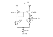
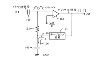
4 インバータ 5 インバータ 100 キャパシタ
101 コンパレータ 102 抵抗 103 キャパシタ
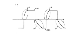
104 チャージポンプ回路 105 充電電流 106 放電電流
110 チャージポンプ回路 111 定電流源 In 入力端子
Out 出力端子 PMOSa,PMOSb Pチャネル型MOSトランジスタ
PMOS1 第1のPチャネル型MOSトランジスタ
PMOS2 第2のPチャネル型MOSトランジスタ
SWa,SWb スイッチング素子
SW1〜SW4 第1のスイッチング素子〜第4のスイッチング素子
Claims (3)
- 入力信号に応じて、キャパシタの充電及び放電を行うチャージポンプ回路において、
第1の電流源と、第2の電流源と、第1のトランジスタと、前記第1のトランジスタとカレントミラー回路を構成する第2のトランジスタと、
入力信号が第1のレベルの時に、前記第1の電流源を前記第1のトランジスタに接続して、前記カレントミラー回路から前記キャパシタに充電電流を出力し、
入力信号が第2のレベルの時に、前記第2の電流源を前記第1のトランジスタに接続し、前記カレントミラー回路の出力を遮断するとともに、前記第1の電流源により前記キャパシタからの放電電流を流すように制御を行うスイッチング回路を備えることを特徴とするチャージポンプ回路。 - 前記第1及び第2の電流源の流す電流の電流値が互いに等しいことを特徴とする請求項1に記載のチャージポンプ回路。
- アナログRF信号の直流成分を除去する第1のキャパシタと、
前記第1のキャパシタを通して入力されたアナログRF信号が第1の入力端子に印加され、第2の入力端子に基準電圧が印加され、前記アナログRF信号と前記基準電圧とを比較して、その比較結果に応じてデジタルRF信号を出力するコンパレータと、
前記第1の入力端子に接続された第2のキャパシタと、
前記コンパレータから出力されたデジタルRF信号に応じて、前記第2のキャパシタの充電及び放電を行うチャージポンプ回路と、を備え、
前記チャージポンプ回路は、第1の電流源と、第2の電流源と、第1のトランジスタと、前記第1のトランジスタとカレントミラー回路を構成する第2のトランジスタと、
前記コンパレータから出力されたデジタルRF信号が第1のレベルの時に、前記第1の電流源を前記第1のトランジスタに接続して、前記カレントミラー回路から前記第2のキャパシタに充電電流を出力し、
前記コンパレータから出力されたデジタルRF信号が第2のレベルの時に、前記第2の電流源を前記第1のトランジスタに接続し、前記カレントミラー回路の出力を遮断するとともに、前記第1の電流源により前記第2のキャパシタからの放電電流を流すように制御を行うスイッチング回路を備えることを特徴とするスライスレベルコントロール回路。
Priority Applications (3)
| Application Number | Priority Date | Filing Date | Title |
|---|---|---|---|
| JP2007147845A JP4657252B2 (ja) | 2007-06-04 | 2007-06-04 | チャージポンプ回路及びスライスレベルコントロール回路 |
| KR1020080052063A KR100977363B1 (ko) | 2007-06-04 | 2008-06-03 | 차지 펌프 회로 및 슬라이스 레벨 컨트롤 회로 |
| US12/132,996 US8058923B2 (en) | 2007-06-04 | 2008-06-04 | Charge pump circuit and slice level control circuit |
Applications Claiming Priority (1)
| Application Number | Priority Date | Filing Date | Title |
|---|---|---|---|
| JP2007147845A JP4657252B2 (ja) | 2007-06-04 | 2007-06-04 | チャージポンプ回路及びスライスレベルコントロール回路 |
Publications (2)
| Publication Number | Publication Date |
|---|---|
| JP2008300012A JP2008300012A (ja) | 2008-12-11 |
| JP4657252B2 true JP4657252B2 (ja) | 2011-03-23 |
Family
ID=40087452
Family Applications (1)
| Application Number | Title | Priority Date | Filing Date |
|---|---|---|---|
| JP2007147845A Expired - Fee Related JP4657252B2 (ja) | 2007-06-04 | 2007-06-04 | チャージポンプ回路及びスライスレベルコントロール回路 |
Country Status (3)
| Country | Link |
|---|---|
| US (1) | US8058923B2 (ja) |
| JP (1) | JP4657252B2 (ja) |
| KR (1) | KR100977363B1 (ja) |
Families Citing this family (4)
| Publication number | Priority date | Publication date | Assignee | Title |
|---|---|---|---|---|
| US8085009B2 (en) * | 2007-08-13 | 2011-12-27 | The Powerwise Group, Inc. | IGBT/FET-based energy savings device for reducing a predetermined amount of voltage using pulse width modulation |
| CN102324931B (zh) * | 2011-05-17 | 2013-04-17 | 西安电子科技大学 | 频率综合器中的电荷泵电路 |
| CN111312313B (zh) * | 2018-12-12 | 2022-02-22 | 北京兆易创新科技股份有限公司 | 一种电荷泵电压快切的电路 |
| CN117457344B (zh) * | 2023-12-22 | 2024-03-08 | 搏世因(北京)高压电气有限公司 | 一种密封散热的干式电容型变压器套管 |
Family Cites Families (14)
| Publication number | Priority date | Publication date | Assignee | Title |
|---|---|---|---|---|
| US6570944B2 (en) * | 2001-06-25 | 2003-05-27 | Rambus Inc. | Apparatus for data recovery in a synchronous chip-to-chip system |
| US20040057548A1 (en) * | 1994-03-18 | 2004-03-25 | Silicon Integrated System Corp. | Quasi-synchronous multi-stage event synchronization apparatus |
| US5473283A (en) * | 1994-11-07 | 1995-12-05 | National Semiconductor Corporation | Cascode switched charge pump circuit |
| JPH09237459A (ja) | 1996-02-29 | 1997-09-09 | Sanyo Electric Co Ltd | 光ディスク用の信号再生回路 |
| US6247138B1 (en) * | 1997-06-12 | 2001-06-12 | Fujitsu Limited | Timing signal generating circuit, semiconductor integrated circuit device and semiconductor integrated circuit system to which the timing signal generating circuit is applied, and signal transmission system |
| JP3356277B2 (ja) * | 1999-09-14 | 2002-12-16 | 日本電気株式会社 | チャージポンプ回路及びpll回路 |
| JP2001319424A (ja) * | 1999-09-24 | 2001-11-16 | Sanyo Electric Co Ltd | 信号処理回路および半導体集積回路 |
| JP3327271B2 (ja) * | 1999-11-15 | 2002-09-24 | 日本電気株式会社 | Pll回路及びデータ読み出し回路 |
| US6429715B1 (en) * | 2000-01-13 | 2002-08-06 | Xilinx, Inc. | Deskewing clock signals for off-chip devices |
| US6218900B1 (en) * | 2000-03-29 | 2001-04-17 | Microchip Technology Incorporated | Operational amplifier phase reversal protection |
| JP2003077135A (ja) * | 2001-08-31 | 2003-03-14 | Matsushita Electric Ind Co Ltd | 光ディスクのrf信号振幅制御装置 |
| US7098714B2 (en) * | 2003-12-08 | 2006-08-29 | Micron Technology, Inc. | Centralizing the lock point of a synchronous circuit |
| JP4412027B2 (ja) * | 2004-03-29 | 2010-02-10 | 日本電気株式会社 | 増幅回路及び表示装置 |
| US7379382B2 (en) * | 2005-10-28 | 2008-05-27 | Micron Technology, Inc. | System and method for controlling timing of output signals |
-
2007
- 2007-06-04 JP JP2007147845A patent/JP4657252B2/ja not_active Expired - Fee Related
-
2008
- 2008-06-03 KR KR1020080052063A patent/KR100977363B1/ko not_active Expired - Fee Related
- 2008-06-04 US US12/132,996 patent/US8058923B2/en active Active
Also Published As
| Publication number | Publication date |
|---|---|
| KR20080106851A (ko) | 2008-12-09 |
| KR100977363B1 (ko) | 2010-08-20 |
| US20080297232A1 (en) | 2008-12-04 |
| JP2008300012A (ja) | 2008-12-11 |
| US8058923B2 (en) | 2011-11-15 |
Similar Documents
| Publication | Publication Date | Title |
|---|---|---|
| US7548047B1 (en) | Pulse width modulated buck voltage regulator with stable feedback control loop | |
| US6985006B2 (en) | Adjusting the strength of output buffers | |
| US8208658B2 (en) | Amplifier apparatus and method | |
| US9722585B2 (en) | Circuit and method to extend a signal comparison voltage range | |
| US8232848B2 (en) | Semiconductor integrated circuit device | |
| US7203149B1 (en) | PLL circuit and data read-out circuit | |
| US20060188048A1 (en) | Clock Extracting Circuit | |
| CN115053196B (zh) | 减轻由高电压电路驱动的低电压参考缓冲器中的可靠性问题 | |
| JP2008300012A (ja) | チャージポンプ回路及びスライスレベルコントロール回路 | |
| JP6902952B2 (ja) | 位相補間器およびタイミング発生器、半導体集積回路 | |
| JP6071521B2 (ja) | 量子化器,比較回路および半導体集積回路 | |
| JP2006222748A (ja) | コンパレータ回路 | |
| US9225294B2 (en) | Amplifier with improved noise reduction | |
| JP4023684B2 (ja) | 周波数電流変換回路、及びそれを備えるイコライザ、光ディスク装置 | |
| JP4872470B2 (ja) | レベルシフタ回路及び情報再生装置 | |
| KR101880491B1 (ko) | 저전력 시간 증폭기 및 그의 동작 방법 | |
| US7609186B1 (en) | Circuit for converting a voltage range of a logic signal | |
| JP5200263B2 (ja) | 半導体集積回路 | |
| JP2007067819A (ja) | 遅延調整回路及び該回路を備えた同期型半導体装置 | |
| JP2008125141A (ja) | D/a変換回路 | |
| JP2007096452A (ja) | レベルシフト回路 | |
| JP5318502B2 (ja) | コンパレータ回路 | |
| JP4100877B2 (ja) | D/a変換回路 | |
| JP2008067042A (ja) | 半導体集積回路装置 | |
| JP2005354142A (ja) | 半導体集積回路及びオペアンプ回路 |
Legal Events
| Date | Code | Title | Description |
|---|---|---|---|
| A621 | Written request for application examination |
Free format text: JAPANESE INTERMEDIATE CODE: A621 Effective date: 20100127 |
|
| A977 | Report on retrieval |
Free format text: JAPANESE INTERMEDIATE CODE: A971007 Effective date: 20101028 |
|
| TRDD | Decision of grant or rejection written | ||
| A01 | Written decision to grant a patent or to grant a registration (utility model) |
Free format text: JAPANESE INTERMEDIATE CODE: A01 Effective date: 20101124 |
|
| A01 | Written decision to grant a patent or to grant a registration (utility model) |
Free format text: JAPANESE INTERMEDIATE CODE: A01 |
|
| A61 | First payment of annual fees (during grant procedure) |
Free format text: JAPANESE INTERMEDIATE CODE: A61 Effective date: 20101221 |
|
| FPAY | Renewal fee payment (event date is renewal date of database) |
Free format text: PAYMENT UNTIL: 20140107 Year of fee payment: 3 |
|
| R151 | Written notification of patent or utility model registration |
Ref document number: 4657252 Country of ref document: JP Free format text: JAPANESE INTERMEDIATE CODE: R151 |
|
| FPAY | Renewal fee payment (event date is renewal date of database) |
Free format text: PAYMENT UNTIL: 20140107 Year of fee payment: 3 |
|
| FPAY | Renewal fee payment (event date is renewal date of database) |
Free format text: PAYMENT UNTIL: 20140107 Year of fee payment: 3 |
|
| S111 | Request for change of ownership or part of ownership |
Free format text: JAPANESE INTERMEDIATE CODE: R313113 |
|
| FPAY | Renewal fee payment (event date is renewal date of database) |
Free format text: PAYMENT UNTIL: 20140107 Year of fee payment: 3 |
|
| R360 | Written notification for declining of transfer of rights |
Free format text: JAPANESE INTERMEDIATE CODE: R360 |
|
| FPAY | Renewal fee payment (event date is renewal date of database) |
Free format text: PAYMENT UNTIL: 20140107 Year of fee payment: 3 |
|
| R370 | Written measure of declining of transfer procedure |
Free format text: JAPANESE INTERMEDIATE CODE: R370 |
|
| R250 | Receipt of annual fees |
Free format text: JAPANESE INTERMEDIATE CODE: R250 |
|
| R250 | Receipt of annual fees |
Free format text: JAPANESE INTERMEDIATE CODE: R250 |
|
| R250 | Receipt of annual fees |
Free format text: JAPANESE INTERMEDIATE CODE: R250 |
|
| R250 | Receipt of annual fees |
Free format text: JAPANESE INTERMEDIATE CODE: R250 |
|
| R250 | Receipt of annual fees |
Free format text: JAPANESE INTERMEDIATE CODE: R250 |
|
| R250 | Receipt of annual fees |
Free format text: JAPANESE INTERMEDIATE CODE: R250 |
|
| R250 | Receipt of annual fees |
Free format text: JAPANESE INTERMEDIATE CODE: R250 |
|
| R250 | Receipt of annual fees |
Free format text: JAPANESE INTERMEDIATE CODE: R250 |
|
| LAPS | Cancellation because of no payment of annual fees |