JP4660632B2 - 半導体記憶装置 - Google Patents
半導体記憶装置 Download PDFInfo
- Publication number
- JP4660632B2 JP4660632B2 JP2010171097A JP2010171097A JP4660632B2 JP 4660632 B2 JP4660632 B2 JP 4660632B2 JP 2010171097 A JP2010171097 A JP 2010171097A JP 2010171097 A JP2010171097 A JP 2010171097A JP 4660632 B2 JP4660632 B2 JP 4660632B2
- Authority
- JP
- Japan
- Prior art keywords
- error correction
- error
- unit
- data
- code
- Prior art date
- Legal status (The legal status is an assumption and is not a legal conclusion. Google has not performed a legal analysis and makes no representation as to the accuracy of the status listed.)
- Expired - Fee Related
Links
Images







Classifications
-
- Y—GENERAL TAGGING OF NEW TECHNOLOGICAL DEVELOPMENTS; GENERAL TAGGING OF CROSS-SECTIONAL TECHNOLOGIES SPANNING OVER SEVERAL SECTIONS OF THE IPC; TECHNICAL SUBJECTS COVERED BY FORMER USPC CROSS-REFERENCE ART COLLECTIONS [XRACs] AND DIGESTS
- Y02—TECHNOLOGIES OR APPLICATIONS FOR MITIGATION OR ADAPTATION AGAINST CLIMATE CHANGE
- Y02D—CLIMATE CHANGE MITIGATION TECHNOLOGIES IN INFORMATION AND COMMUNICATION TECHNOLOGIES [ICT], I.E. INFORMATION AND COMMUNICATION TECHNOLOGIES AIMING AT THE REDUCTION OF THEIR OWN ENERGY USE
- Y02D10/00—Energy efficient computing, e.g. low power processors, power management or thermal management
Landscapes
- For Increasing The Reliability Of Semiconductor Memories (AREA)
- Techniques For Improving Reliability Of Storages (AREA)
Description
図2は、誤り訂正回路1のデータ書き込みに関する主要部を示すブロック図である。誤り訂正回路1は、それぞれが所定の大きさの複数の書き込みデータのそれぞれを1つの単位として、誤り訂正符号を生成するとともに、複数の書き込みデータ全体を1つの単位として別の誤り訂正符号を生成する。書き込みデータの数は、達成することが望まれる誤り訂正能力および採用される誤り訂正符号に応じて決定され、以下、書き込みデータが8個である例について説明する。
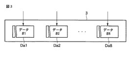
次に、誤り訂正回路1の、データ書き込み時の動作について図3乃至図6を参照して説明する。図3乃至図6は、書き込みの際の一時記憶回路3内のデータの状態を概略的に順に示している。
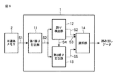
図6は、誤り訂正回路1のデータ読み出しに関する主要部を示すブロック図である。
Claims (3)
- 複数の第1データ内の誤りをそれぞれ検出するための複数の検出符号を生成する検出符号生成部と、
各第1データとこれに対応する検出符号とから第1単位データが構成され、複数の第1単位データ内の誤りをそれぞれ訂正するための複数の第1訂正符号を生成する第1訂正符号生成部と、
前記複数の第1単位データから第2単位データが構成され、この第2単位データ内の誤りを訂正するための第2訂正符号を生成する第2訂正符号生成部と、
前記第2単位データ、前記複数の第1訂正符号、及び前記第2訂正符号を不揮発に格納する半導体メモリと、
前記複数の第1訂正符号を用いて、前記複数の第1単位データ内の誤りをそれぞれ訂正する第1訂正部と、
前記複数の検出符号を用いて、前記第1訂正部により訂正された複数の第1データ内の誤りをそれぞれ検出し、かつ前記訂正された複数の第1データのそれぞれについての誤りの有無を示す第1誤り情報を生成する検出部と、
前記第1誤り情報および前記第2訂正符号を用いて、前記訂正された複数の第1データのうち誤りを含んだものに対してチェン探索を行い、誤りを訂正する第2訂正部と、
を具備し、
前記第2訂正符号の誤り訂正能力は、前記第1訂正符号の誤り訂正能力よりも高いことを特徴とする半導体記憶装置。 - 前記第2訂正部は、前記第1訂正部により訂正された複数の第1データ内に誤りが存在しない場合に、訂正処理を停止することを特徴とする請求項1に記載の半導体記憶装置。
- 前記半導体メモリは、NAND型フラッシュメモリであることを特徴とする請求項1又は2に記載の半導体記憶装置。
Priority Applications (1)
| Application Number | Priority Date | Filing Date | Title |
|---|---|---|---|
| JP2010171097A JP4660632B2 (ja) | 2010-07-29 | 2010-07-29 | 半導体記憶装置 |
Applications Claiming Priority (1)
| Application Number | Priority Date | Filing Date | Title |
|---|---|---|---|
| JP2010171097A JP4660632B2 (ja) | 2010-07-29 | 2010-07-29 | 半導体記憶装置 |
Related Parent Applications (1)
| Application Number | Title | Priority Date | Filing Date |
|---|---|---|---|
| JP2007225996A Division JP4564520B2 (ja) | 2007-08-31 | 2007-08-31 | 半導体記憶装置およびその制御方法 |
Publications (2)
| Publication Number | Publication Date |
|---|---|
| JP2010238363A JP2010238363A (ja) | 2010-10-21 |
| JP4660632B2 true JP4660632B2 (ja) | 2011-03-30 |
Family
ID=43092532
Family Applications (1)
| Application Number | Title | Priority Date | Filing Date |
|---|---|---|---|
| JP2010171097A Expired - Fee Related JP4660632B2 (ja) | 2010-07-29 | 2010-07-29 | 半導体記憶装置 |
Country Status (1)
| Country | Link |
|---|---|
| JP (1) | JP4660632B2 (ja) |
Families Citing this family (6)
| Publication number | Priority date | Publication date | Assignee | Title |
|---|---|---|---|---|
| JP4564520B2 (ja) | 2007-08-31 | 2010-10-20 | 株式会社東芝 | 半導体記憶装置およびその制御方法 |
| JP4672743B2 (ja) * | 2008-03-01 | 2011-04-20 | 株式会社東芝 | 誤り訂正装置および誤り訂正方法 |
| JP4686645B2 (ja) * | 2010-07-29 | 2011-05-25 | 株式会社東芝 | 半導体記憶装置およびその制御方法 |
| US8464137B2 (en) * | 2010-12-03 | 2013-06-11 | International Business Machines Corporation | Probabilistic multi-tier error correction in not-and (NAND) flash memory |
| JP6346123B2 (ja) | 2015-05-25 | 2018-06-20 | 東芝メモリ株式会社 | コントローラ、制御方法 |
| US11216333B2 (en) | 2018-10-16 | 2022-01-04 | Micron Technology, Inc. | Methods and devices for error correction |
-
2010
- 2010-07-29 JP JP2010171097A patent/JP4660632B2/ja not_active Expired - Fee Related
Also Published As
| Publication number | Publication date |
|---|---|
| JP2010238363A (ja) | 2010-10-21 |
Similar Documents
| Publication | Publication Date | Title |
|---|---|---|
| JP4564520B2 (ja) | 半導体記憶装置およびその制御方法 | |
| JP4538034B2 (ja) | 半導体記憶装置、及びその制御方法 | |
| JP4660632B2 (ja) | 半導体記憶装置 | |
| JP4686645B2 (ja) | 半導体記憶装置およびその制御方法 |
Legal Events
| Date | Code | Title | Description |
|---|---|---|---|
| A621 | Written request for application examination |
Free format text: JAPANESE INTERMEDIATE CODE: A621 Effective date: 20100729 |
|
| A521 | Request for written amendment filed |
Free format text: JAPANESE INTERMEDIATE CODE: A523 Effective date: 20100819 |
|
| A871 | Explanation of circumstances concerning accelerated examination |
Free format text: JAPANESE INTERMEDIATE CODE: A871 Effective date: 20101110 |
|
| TRDD | Decision of grant or rejection written | ||
| A975 | Report on accelerated examination |
Free format text: JAPANESE INTERMEDIATE CODE: A971005 Effective date: 20101124 |
|
| A01 | Written decision to grant a patent or to grant a registration (utility model) |
Free format text: JAPANESE INTERMEDIATE CODE: A01 Effective date: 20101130 |
|
| A01 | Written decision to grant a patent or to grant a registration (utility model) |
Free format text: JAPANESE INTERMEDIATE CODE: A01 |
|
| A61 | First payment of annual fees (during grant procedure) |
Free format text: JAPANESE INTERMEDIATE CODE: A61 Effective date: 20101228 |
|
| FPAY | Renewal fee payment (event date is renewal date of database) |
Free format text: PAYMENT UNTIL: 20140107 Year of fee payment: 3 |
|
| R151 | Written notification of patent or utility model registration |
Ref document number: 4660632 Country of ref document: JP Free format text: JAPANESE INTERMEDIATE CODE: R151 |
|
| FPAY | Renewal fee payment (event date is renewal date of database) |
Free format text: PAYMENT UNTIL: 20140107 Year of fee payment: 3 |
|
| S111 | Request for change of ownership or part of ownership |
Free format text: JAPANESE INTERMEDIATE CODE: R313111 |
|
| R350 | Written notification of registration of transfer |
Free format text: JAPANESE INTERMEDIATE CODE: R350 |
|
| LAPS | Cancellation because of no payment of annual fees |