JP4669246B2 - 半導体装置およびその製造方法 - Google Patents
半導体装置およびその製造方法 Download PDFInfo
- Publication number
- JP4669246B2 JP4669246B2 JP2004236770A JP2004236770A JP4669246B2 JP 4669246 B2 JP4669246 B2 JP 4669246B2 JP 2004236770 A JP2004236770 A JP 2004236770A JP 2004236770 A JP2004236770 A JP 2004236770A JP 4669246 B2 JP4669246 B2 JP 4669246B2
- Authority
- JP
- Japan
- Prior art keywords
- film
- semiconductor device
- transistor
- capacitive
- capacitor
- Prior art date
- Legal status (The legal status is an assumption and is not a legal conclusion. Google has not performed a legal analysis and makes no representation as to the accuracy of the status listed.)
- Expired - Fee Related
Links
Images



Classifications
-
- H—ELECTRICITY
- H10—SEMICONDUCTOR DEVICES; ELECTRIC SOLID-STATE DEVICES NOT OTHERWISE PROVIDED FOR
- H10D—INORGANIC ELECTRIC SEMICONDUCTOR DEVICES
- H10D1/00—Resistors, capacitors or inductors
- H10D1/60—Capacitors
- H10D1/68—Capacitors having no potential barriers
-
- H—ELECTRICITY
- H10—SEMICONDUCTOR DEVICES; ELECTRIC SOLID-STATE DEVICES NOT OTHERWISE PROVIDED FOR
- H10D—INORGANIC ELECTRIC SEMICONDUCTOR DEVICES
- H10D84/00—Integrated devices formed in or on semiconductor substrates that comprise only semiconducting layers, e.g. on Si wafers or on GaAs-on-Si wafers
- H10D84/80—Integrated devices formed in or on semiconductor substrates that comprise only semiconducting layers, e.g. on Si wafers or on GaAs-on-Si wafers characterised by the integration of at least one component covered by groups H10D12/00 or H10D30/00, e.g. integration of IGFETs
- H10D84/811—Combinations of field-effect devices and one or more diodes, capacitors or resistors
-
- H—ELECTRICITY
- H10—SEMICONDUCTOR DEVICES; ELECTRIC SOLID-STATE DEVICES NOT OTHERWISE PROVIDED FOR
- H10D—INORGANIC ELECTRIC SEMICONDUCTOR DEVICES
- H10D84/00—Integrated devices formed in or on semiconductor substrates that comprise only semiconducting layers, e.g. on Si wafers or on GaAs-on-Si wafers
- H10D84/80—Integrated devices formed in or on semiconductor substrates that comprise only semiconducting layers, e.g. on Si wafers or on GaAs-on-Si wafers characterised by the integration of at least one component covered by groups H10D12/00 or H10D30/00, e.g. integration of IGFETs
- H10D84/811—Combinations of field-effect devices and one or more diodes, capacitors or resistors
- H10D84/813—Combinations of field-effect devices and capacitor only
Landscapes
- Semiconductor Integrated Circuits (AREA)
- Metal-Oxide And Bipolar Metal-Oxide Semiconductor Integrated Circuits (AREA)
- Internal Circuitry In Semiconductor Integrated Circuit Devices (AREA)
Description
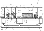
表層に導電層が設けられた半導体基板と、
前記半導体基板の表面のうち平坦な部分上に設けられた容量膜と、
前記容量膜上に設けられ、前記容量膜を挟んで対向する前記導電層との間で容量素子を構成する上部電極と、
前記半導体基板に設けられたトランジスタと、
前記トランジスタ上に設けられた層間窒化膜と、
前記層間窒化膜上に設けられた絶縁膜と、を備え、
前記容量膜は、前記トランジスタのゲート絶縁膜に比して厚く、
前記絶縁膜は、前記容量膜と一体となって設けられている、半導体装置が提供される。
半導体基板に、不純物を導入して形成される不純物拡散層を形成する導電層形成工程と、
前記半導体基板上にトランジスタを形成する工程と、
前記トランジスタ上に層間窒化膜を形成する工程と、
前記層間窒化膜上、および前記導電層が形成された前記半導体基板の表面のうち平坦な部分上に容量膜を形成する容量膜形成工程と、
前記容量膜上に、前記容量膜を挟んで対向する前記導電層との間で容量素子を構成する上部電極を形成する電極形成工程と、をこの順番で含み、
前記容量膜は、前記トランジスタのゲート絶縁膜に比して厚く形成されている、半導体装置の製造方法が提供される。
1a 半導体装置
1b 半導体装置
10 半導体基板
20 容量素子形成領域
22 N型ウエル
23 拡散層
24,25 容量膜
24a 金属元素拡散防止膜
26,27 上部電極
30 トランジスタ形成領域
32 P型ウエル
34 ソース・ドレイン領域
36 ゲート絶縁膜
38 ゲート電極
40 サイドウォール
42 層間窒化膜
44 絶縁膜
52,54,56,58 コンタクト
60 層間絶縁膜
72 シリサイドブロック
74,76 レジスト
62,64,66,68 STI
Claims (7)
- 表層に導電層が設けられた半導体基板と、
前記半導体基板の表面のうち平坦な部分上に設けられた容量膜と、
前記容量膜上に設けられ、前記容量膜を挟んで対向する前記導電層との間で容量素子を構成する上部電極と、
前記半導体基板に設けられたトランジスタと、
前記トランジスタ上に設けられた層間窒化膜と、
前記層間窒化膜上に設けられた絶縁膜と、を備え、
前記容量膜は、前記トランジスタのゲート絶縁膜に比して厚く、
前記絶縁膜は、前記容量膜と一体となって設けられている、半導体装置。 - 請求項1に記載の半導体装置において、
前記容量膜は、前記半導体基板側の表層に設けられた、金属元素の拡散を防止する絶縁膜を有する、半導体装置。 - 請求項1または2に記載の半導体装置において、
前記容量膜は、シリコン酸化膜よりも高い誘電率をもつ高誘電率膜である、半導体装置。 - 請求項1から3の何れか一項に記載の半導体装置において、
前記容量膜は、前記トランジスタのゲート絶縁膜に比して電気的換算膜厚が薄い、半導体装置。 - 請求項1から4の何れか一項に記載の半導体装置において、
前記半導体基板における前記容量膜が設けられている部分は、シリサイド化されていない、半導体装置。 - 半導体基板に、不純物を導入して形成される不純物拡散層を形成する導電層形成工程と、
前記半導体基板上にトランジスタを形成する工程と、
前記トランジスタ上に層間窒化膜を形成する工程と、
前記層間窒化膜上、および前記導電層が形成された前記半導体基板の表面のうち平坦な部分上に容量膜を形成する容量膜形成工程と、
前記容量膜上に、前記容量膜を挟んで対向する前記導電層との間で容量素子を構成する上部電極を形成する電極形成工程と、をこの順番で含み、
前記容量膜は、前記トランジスタのゲート絶縁膜に比して厚く形成されている、半導体装置の製造方法。 - 請求項6に記載の半導体装置の製造方法において、
前記半導体基板は、トランジスタ形成領域と容量素子形成領域とを有し、
前記トランジスタ形成領域に前記トランジスタを形成する工程と、
前記容量素子形成領域にシリサイドブロックを形成するシリサイドブロック形成工程と、をこの順番で含み、
前記トランジスタを形成する前記工程および前記シリサイドブロック形成工程よりも後に、前記半導体基板の表面における前記シリサイドブロックが形成されていない部分をシリサイド化するシリサイド工程を行い、
前記シリサイド工程よりも後に前記シリサイドブロックを除去するシリサイドブロック除去工程を行い、
前記容量膜形成工程は、前記シリサイドブロック除去工程よりも後に実行される、半導体装置の製造方法。
Priority Applications (2)
| Application Number | Priority Date | Filing Date | Title |
|---|---|---|---|
| JP2004236770A JP4669246B2 (ja) | 2004-08-16 | 2004-08-16 | 半導体装置およびその製造方法 |
| US11/204,163 US7498626B2 (en) | 2004-08-16 | 2005-08-16 | Semiconductor device and method of manufacturing the same |
Applications Claiming Priority (1)
| Application Number | Priority Date | Filing Date | Title |
|---|---|---|---|
| JP2004236770A JP4669246B2 (ja) | 2004-08-16 | 2004-08-16 | 半導体装置およびその製造方法 |
Publications (2)
| Publication Number | Publication Date |
|---|---|
| JP2006054402A JP2006054402A (ja) | 2006-02-23 |
| JP4669246B2 true JP4669246B2 (ja) | 2011-04-13 |
Family
ID=35799190
Family Applications (1)
| Application Number | Title | Priority Date | Filing Date |
|---|---|---|---|
| JP2004236770A Expired - Fee Related JP4669246B2 (ja) | 2004-08-16 | 2004-08-16 | 半導体装置およびその製造方法 |
Country Status (2)
| Country | Link |
|---|---|
| US (1) | US7498626B2 (ja) |
| JP (1) | JP4669246B2 (ja) |
Families Citing this family (8)
| Publication number | Priority date | Publication date | Assignee | Title |
|---|---|---|---|---|
| US20070141776A1 (en) * | 2005-12-19 | 2007-06-21 | Jung-Ching Chen | Semiconductor device having capacitor and fabricating method thereof |
| JP2011138885A (ja) * | 2009-12-28 | 2011-07-14 | Renesas Electronics Corp | 半導体装置及び半導体装置の製造方法 |
| US9412883B2 (en) | 2011-11-22 | 2016-08-09 | Taiwan Semiconductor Manufacturing Company, Ltd. | Methods and apparatus for MOS capacitors in replacement gate process |
| CN104752422B (zh) * | 2013-12-30 | 2017-11-03 | 中芯国际集成电路制造(上海)有限公司 | 半导体器件及其形成方法 |
| US10418364B2 (en) * | 2016-08-31 | 2019-09-17 | Globalfoundries Inc. | Semiconductor device structure with self-aligned capacitor device |
| US10680120B2 (en) * | 2018-04-05 | 2020-06-09 | Vanguard International Semiconductor Corporation | Semiconductor device and method for manufacturing the same |
| US11004785B2 (en) * | 2019-08-21 | 2021-05-11 | Stmicroelectronics (Rousset) Sas | Co-integrated vertically structured capacitive element and fabrication process |
| US12371615B2 (en) * | 2020-05-08 | 2025-07-29 | Sharp Kabushiki Kaisha | Method of treating quantum dot-containing aqueous solution |
Family Cites Families (17)
| Publication number | Priority date | Publication date | Assignee | Title |
|---|---|---|---|---|
| US4811076A (en) * | 1985-05-01 | 1989-03-07 | Texas Instruments Incorporated | Device and process with doubled capacitors |
| JP2633605B2 (ja) * | 1988-03-02 | 1997-07-23 | 株式会社東芝 | 半導体装置用キャパシタ |
| JP2735407B2 (ja) * | 1990-08-30 | 1998-04-02 | 株式会社東芝 | 半導体装置およびその製造方法 |
| JP2861604B2 (ja) * | 1992-03-11 | 1999-02-24 | 富士通株式会社 | 半導体装置の製造方法 |
| JPH06291262A (ja) * | 1993-03-31 | 1994-10-18 | Sony Corp | 半導体装置の製造方法 |
| US5457065A (en) * | 1994-12-14 | 1995-10-10 | United Microelectronics Corporation | method of manufacturing a new DRAM capacitor structure having increased capacitance |
| JP3369827B2 (ja) * | 1995-01-30 | 2003-01-20 | 株式会社東芝 | 半導体装置及びその製造方法 |
| JPH118352A (ja) * | 1997-06-14 | 1999-01-12 | Toshiba Microelectron Corp | 半導体集積回路装置及びその製造方法 |
| JP2000174216A (ja) * | 1998-10-02 | 2000-06-23 | Sony Corp | 半導体装置の製造方法 |
| JP2000124336A (ja) * | 1998-10-12 | 2000-04-28 | Sony Corp | 半導体装置及び半導体装置の製造方法 |
| JP2001308274A (ja) * | 2000-04-24 | 2001-11-02 | Nec Corp | 電圧履歴記録素子およびそれを用いた電子デバイスの印加電圧履歴記録方法 |
| JP2002222924A (ja) | 2001-01-25 | 2002-08-09 | Sharp Corp | 半導体装置の製造方法 |
| KR100422565B1 (ko) | 2001-06-12 | 2004-03-12 | 주식회사 하이닉스반도체 | 반도체 소자의 캐패시터 제조방법 |
| US6511873B2 (en) * | 2001-06-15 | 2003-01-28 | International Business Machines Corporation | High-dielectric constant insulators for FEOL capacitors |
| JP3778065B2 (ja) * | 2001-11-22 | 2006-05-24 | ソニー株式会社 | 半導体装置の製造方法 |
| DE10240423B4 (de) * | 2002-09-02 | 2007-02-22 | Advanced Micro Devices, Inc., Sunnyvale | Halbleiterelement mit einem Feldeffekttransistor und einem passiven Kondensator mit reduziertem Leckstrom und einer verbesserten Kapazität pro Einheitsfläche und Verfahren zu dessen Herstellung |
| JP5148814B2 (ja) * | 2002-09-02 | 2013-02-20 | アドバンスト・マイクロ・ディバイシズ・インコーポレイテッド | 漏れ電流を減少させ、単位面積あたりのキャパシタンスを改善した、電界効果トランジスタおよび受動コンデンサを有する半導体装置 |
-
2004
- 2004-08-16 JP JP2004236770A patent/JP4669246B2/ja not_active Expired - Fee Related
-
2005
- 2005-08-16 US US11/204,163 patent/US7498626B2/en not_active Expired - Lifetime
Also Published As
| Publication number | Publication date |
|---|---|
| US20060033139A1 (en) | 2006-02-16 |
| JP2006054402A (ja) | 2006-02-23 |
| US7498626B2 (en) | 2009-03-03 |
Similar Documents
| Publication | Publication Date | Title |
|---|---|---|
| US20080308876A1 (en) | Semiconductor device and method of manufacturing the same | |
| US9105720B2 (en) | Semiconductor device having metal gate and manufacturing method thereof | |
| US8643069B2 (en) | Semiconductor device having metal gate and manufacturing method thereof | |
| US10068797B2 (en) | Semiconductor process for forming plug | |
| TWI656603B (zh) | 半導體元件及其製程 | |
| WO2010095186A1 (ja) | 半導体装置及びその製造方法 | |
| US11295955B2 (en) | Transistor | |
| CN100539150C (zh) | 半导体装置制造方法 | |
| CN103247672B (zh) | 半导体器件及其制造方法 | |
| US20120256275A1 (en) | Metal gate structure and manufacturing method thereof | |
| JP4954508B2 (ja) | 半導体装置 | |
| JP4669246B2 (ja) | 半導体装置およびその製造方法 | |
| US8486790B2 (en) | Manufacturing method for metal gate | |
| US20060157750A1 (en) | Semiconductor device having etch-resistant L-shaped spacer and fabrication method thereof | |
| US20070200185A1 (en) | Semiconductor device and method for fabricating the same | |
| JP5410398B2 (ja) | 半導体装置 | |
| US12125909B2 (en) | Asymmetric semiconductor device including LDD region and manufacturing method thereof | |
| TWI695477B (zh) | 半導體結構及其製作方法 | |
| US8008728B2 (en) | Semiconductor device and manufacturing method of semiconductor device | |
| TWI591730B (zh) | 半導體元件與製作方法 | |
| JP4673589B2 (ja) | 半導体装置およびその製造方法 | |
| JP3937894B2 (ja) | 半導体装置 | |
| TWI538143B (zh) | 薄膜電阻結構 | |
| TWI402920B (zh) | 半導體裝置及其製造方法 | |
| TWI520307B (zh) | 電阻及其製作方法 |
Legal Events
| Date | Code | Title | Description |
|---|---|---|---|
| A621 | Written request for application examination |
Free format text: JAPANESE INTERMEDIATE CODE: A621 Effective date: 20070712 |
|
| A977 | Report on retrieval |
Free format text: JAPANESE INTERMEDIATE CODE: A971007 Effective date: 20100601 |
|
| A131 | Notification of reasons for refusal |
Free format text: JAPANESE INTERMEDIATE CODE: A131 Effective date: 20100608 |
|
| A521 | Request for written amendment filed |
Free format text: JAPANESE INTERMEDIATE CODE: A523 Effective date: 20100802 |
|
| A131 | Notification of reasons for refusal |
Free format text: JAPANESE INTERMEDIATE CODE: A131 Effective date: 20100914 |
|
| A521 | Request for written amendment filed |
Free format text: JAPANESE INTERMEDIATE CODE: A523 Effective date: 20101102 |
|
| TRDD | Decision of grant or rejection written | ||
| A01 | Written decision to grant a patent or to grant a registration (utility model) |
Free format text: JAPANESE INTERMEDIATE CODE: A01 Effective date: 20110111 |
|
| A01 | Written decision to grant a patent or to grant a registration (utility model) |
Free format text: JAPANESE INTERMEDIATE CODE: A01 |
|
| A61 | First payment of annual fees (during grant procedure) |
Free format text: JAPANESE INTERMEDIATE CODE: A61 Effective date: 20110114 |
|
| FPAY | Renewal fee payment (event date is renewal date of database) |
Free format text: PAYMENT UNTIL: 20140121 Year of fee payment: 3 |
|
| R150 | Certificate of patent or registration of utility model |
Ref document number: 4669246 Country of ref document: JP Free format text: JAPANESE INTERMEDIATE CODE: R150 Free format text: JAPANESE INTERMEDIATE CODE: R150 |
|
| S531 | Written request for registration of change of domicile |
Free format text: JAPANESE INTERMEDIATE CODE: R313531 |
|
| R350 | Written notification of registration of transfer |
Free format text: JAPANESE INTERMEDIATE CODE: R350 |
|
| LAPS | Cancellation because of no payment of annual fees |