JP4671748B2 - 発光装置用配線基板および発光装置 - Google Patents
発光装置用配線基板および発光装置 Download PDFInfo
- Publication number
- JP4671748B2 JP4671748B2 JP2005126108A JP2005126108A JP4671748B2 JP 4671748 B2 JP4671748 B2 JP 4671748B2 JP 2005126108 A JP2005126108 A JP 2005126108A JP 2005126108 A JP2005126108 A JP 2005126108A JP 4671748 B2 JP4671748 B2 JP 4671748B2
- Authority
- JP
- Japan
- Prior art keywords
- light
- light emitting
- emitting device
- substrate
- transparent electrode
- Prior art date
- Legal status (The legal status is an assumption and is not a legal conclusion. Google has not performed a legal analysis and makes no representation as to the accuracy of the status listed.)
- Expired - Fee Related
Links
Images
Classifications
-
- H—ELECTRICITY
- H10—SEMICONDUCTOR DEVICES; ELECTRIC SOLID-STATE DEVICES NOT OTHERWISE PROVIDED FOR
- H10W—GENERIC PACKAGES, INTERCONNECTIONS, CONNECTORS OR OTHER CONSTRUCTIONAL DETAILS OF DEVICES COVERED BY CLASS H10
- H10W72/00—Interconnections or connectors in packages
- H10W72/851—Dispositions of multiple connectors or interconnections
- H10W72/874—On different surfaces
- H10W72/884—Die-attach connectors and bond wires
-
- H—ELECTRICITY
- H10—SEMICONDUCTOR DEVICES; ELECTRIC SOLID-STATE DEVICES NOT OTHERWISE PROVIDED FOR
- H10W—GENERIC PACKAGES, INTERCONNECTIONS, CONNECTORS OR OTHER CONSTRUCTIONAL DETAILS OF DEVICES COVERED BY CLASS H10
- H10W90/00—Package configurations
- H10W90/701—Package configurations characterised by the relative positions of pads or connectors relative to package parts
- H10W90/731—Package configurations characterised by the relative positions of pads or connectors relative to package parts of die-attach connectors
- H10W90/734—Package configurations characterised by the relative positions of pads or connectors relative to package parts of die-attach connectors between a chip and a stacked insulating package substrate, interposer or RDL
-
- H—ELECTRICITY
- H10—SEMICONDUCTOR DEVICES; ELECTRIC SOLID-STATE DEVICES NOT OTHERWISE PROVIDED FOR
- H10W—GENERIC PACKAGES, INTERCONNECTIONS, CONNECTORS OR OTHER CONSTRUCTIONAL DETAILS OF DEVICES COVERED BY CLASS H10
- H10W90/00—Package configurations
- H10W90/701—Package configurations characterised by the relative positions of pads or connectors relative to package parts
- H10W90/751—Package configurations characterised by the relative positions of pads or connectors relative to package parts of bond wires
- H10W90/754—Package configurations characterised by the relative positions of pads or connectors relative to package parts of bond wires between a chip and a stacked insulating package substrate, interposer or RDL
Landscapes
- Led Device Packages (AREA)
Description
酸化亜鉛を含有した材料からなることがより望ましい。
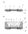
3・・・透明電極
5・・・発光素子
7・・・搭載部
9・・・発光装置用配線基板
21・・・波長変換層
23・・・発光装置
Claims (9)
- 発光素子を搭載するための搭載部が形成され前記発光素子から発せられた励起光が反射する基板と、前記搭載部の周囲に位置する前記基板上であって前記搭載部に搭載された発光素子から発せられる励起光が照射される部位に設けられた透明電極と、を具備することを特徴とする発光装置用配線基板。
- 前記透明電極が、酸化インジウム・スズ、または、酸化亜鉛を含有することを特徴とする請求項1に記載の発光装置用配線基板。
- 前記透明電極の全光線透過率が、80%以上であることを特徴とする請求項1又は2に記載の発光装置用配線基板。
- 前記基板が、白色であることを特徴とする請求項1乃至3のうちいずれかに記載の発光装置用配線基板。
- 前記基板が、セラミック焼結体であることを特徴とする請求項1乃至4のうちいずれかに記載の発光装置用配線基板。
- 請求項1乃至5のうちいずれかに記載の発光装置用配線基板の前記搭載部に、発光素子を搭載してなることを特徴とする発光装置。
- 前記透明電極の透過スペクトルのピーク波長と、前記発光素子から発せられる励起光のピーク波長との差が、30nm以下であることを特徴とする請求項6に記載の発光装置。
- 前記透明電極の反射スペクトルのピーク波長と、前記透明電極を表面に形成してなる前記基板表面の反射スペクトルのピーク波長との差が、30nm以下であることを特徴とする請求項6又は7に記載の発光装置。
- 前記発光装置が、前記発光素子から発する励起光の少なくとも一部を吸収し、可視光を出力光とする波長変換器を備えることを特徴とする請求項6乃至8のうちいずれかに記載の発光装置。
Priority Applications (1)
| Application Number | Priority Date | Filing Date | Title |
|---|---|---|---|
| JP2005126108A JP4671748B2 (ja) | 2005-04-25 | 2005-04-25 | 発光装置用配線基板および発光装置 |
Applications Claiming Priority (1)
| Application Number | Priority Date | Filing Date | Title |
|---|---|---|---|
| JP2005126108A JP4671748B2 (ja) | 2005-04-25 | 2005-04-25 | 発光装置用配線基板および発光装置 |
Publications (2)
| Publication Number | Publication Date |
|---|---|
| JP2006303347A JP2006303347A (ja) | 2006-11-02 |
| JP4671748B2 true JP4671748B2 (ja) | 2011-04-20 |
Family
ID=37471249
Family Applications (1)
| Application Number | Title | Priority Date | Filing Date |
|---|---|---|---|
| JP2005126108A Expired - Fee Related JP4671748B2 (ja) | 2005-04-25 | 2005-04-25 | 発光装置用配線基板および発光装置 |
Country Status (1)
| Country | Link |
|---|---|
| JP (1) | JP4671748B2 (ja) |
Family Cites Families (5)
| Publication number | Priority date | Publication date | Assignee | Title |
|---|---|---|---|---|
| JP2001217456A (ja) * | 2000-02-03 | 2001-08-10 | Sharp Corp | 窒化ガリウム系化合物半導体発光素子 |
| JP4028152B2 (ja) * | 2000-03-27 | 2007-12-26 | 株式会社東芝 | 半導体発光素子 |
| JP4163932B2 (ja) * | 2002-10-28 | 2008-10-08 | 京セラ株式会社 | 発光素子収納用パッケージおよび発光装置 |
| JP4604488B2 (ja) * | 2003-12-26 | 2011-01-05 | 日亜化学工業株式会社 | 窒化物半導体発光素子およびその製造方法 |
| JP3852462B2 (ja) * | 2004-09-27 | 2006-11-29 | 日亜化学工業株式会社 | 発光装置及びその形成方法 |
-
2005
- 2005-04-25 JP JP2005126108A patent/JP4671748B2/ja not_active Expired - Fee Related
Also Published As
| Publication number | Publication date |
|---|---|
| JP2006303347A (ja) | 2006-11-02 |
Similar Documents
| Publication | Publication Date | Title |
|---|---|---|
| JP5422721B2 (ja) | 白色ledランプ、バックライトおよび照明装置 | |
| JP5468985B2 (ja) | 照明装置 | |
| JP3866092B2 (ja) | 波長変換注型材料の製造方法 | |
| US8459840B2 (en) | Semiconductor light emitting apparatus and light source apparatus using the same | |
| JP5113820B2 (ja) | 発光装置 | |
| TWI407589B (zh) | White light emitting diodes and the use of its backlight and liquid crystal display device | |
| JP2011071404A (ja) | 発光装置および照明装置 | |
| JP5810301B2 (ja) | 照明装置 | |
| JP5036332B2 (ja) | 発光装置および色変換フィルター | |
| WO2009128468A1 (ja) | 白色発光装置、バックライト、液晶表示装置および照明装置 | |
| JP2011159832A (ja) | 半導体発光装置 | |
| KR20130002270A (ko) | 평면 발광 모듈 | |
| WO2008027773A2 (en) | White light unit, backlight unit and liquid crystal display device using the same | |
| JP2010225960A (ja) | 発光装置および照明装置 | |
| JP2011155125A (ja) | 発光装置および照明装置 | |
| JP2010199273A (ja) | 発光装置および照明装置 | |
| JP2016157795A (ja) | 発光モジュール | |
| JP5828100B2 (ja) | 発光装置及びそれを用いる照明装置 | |
| JP4671748B2 (ja) | 発光装置用配線基板および発光装置 | |
| JP4949793B2 (ja) | 蛍光体及び波長変換器ならびに発光装置 | |
| JP5662821B2 (ja) | 蛍光体及び発光装置 | |
| JP2011159770A (ja) | 白色半導体発光装置 | |
| JP2013026590A (ja) | 発光装置の製造方法 | |
| JP2011159769A (ja) | 半導体発光装置 | |
| JP2009032683A (ja) | 発光装置 |
Legal Events
| Date | Code | Title | Description |
|---|---|---|---|
| A621 | Written request for application examination |
Free format text: JAPANESE INTERMEDIATE CODE: A621 Effective date: 20080218 |
|
| A977 | Report on retrieval |
Free format text: JAPANESE INTERMEDIATE CODE: A971007 Effective date: 20100914 |
|
| A131 | Notification of reasons for refusal |
Free format text: JAPANESE INTERMEDIATE CODE: A131 Effective date: 20100921 |
|
| A521 | Request for written amendment filed |
Free format text: JAPANESE INTERMEDIATE CODE: A523 Effective date: 20101119 |
|
| TRDD | Decision of grant or rejection written | ||
| A01 | Written decision to grant a patent or to grant a registration (utility model) |
Free format text: JAPANESE INTERMEDIATE CODE: A01 Effective date: 20101221 |
|
| A01 | Written decision to grant a patent or to grant a registration (utility model) |
Free format text: JAPANESE INTERMEDIATE CODE: A01 |
|
| A61 | First payment of annual fees (during grant procedure) |
Free format text: JAPANESE INTERMEDIATE CODE: A61 Effective date: 20110118 |
|
| R150 | Certificate of patent or registration of utility model |
Ref document number: 4671748 Country of ref document: JP Free format text: JAPANESE INTERMEDIATE CODE: R150 |
|
| FPAY | Renewal fee payment (event date is renewal date of database) |
Free format text: PAYMENT UNTIL: 20140128 Year of fee payment: 3 |
|
| LAPS | Cancellation because of no payment of annual fees |