JP4678143B2 - 光スイッチ - Google Patents
光スイッチ Download PDFInfo
- Publication number
- JP4678143B2 JP4678143B2 JP2004167325A JP2004167325A JP4678143B2 JP 4678143 B2 JP4678143 B2 JP 4678143B2 JP 2004167325 A JP2004167325 A JP 2004167325A JP 2004167325 A JP2004167325 A JP 2004167325A JP 4678143 B2 JP4678143 B2 JP 4678143B2
- Authority
- JP
- Japan
- Prior art keywords
- optical
- optical waveguide
- layer
- quantum
- optical switch
- Prior art date
- Legal status (The legal status is an assumption and is not a legal conclusion. Google has not performed a legal analysis and makes no representation as to the accuracy of the status listed.)
- Expired - Fee Related
Links
Images




Classifications
-
- G—PHYSICS
- G02—OPTICS
- G02F—OPTICAL DEVICES OR ARRANGEMENTS FOR THE CONTROL OF LIGHT BY MODIFICATION OF THE OPTICAL PROPERTIES OF THE MEDIA OF THE ELEMENTS INVOLVED THEREIN; NON-LINEAR OPTICS; FREQUENCY-CHANGING OF LIGHT; OPTICAL LOGIC ELEMENTS; OPTICAL ANALOGUE/DIGITAL CONVERTERS
- G02F1/00—Devices or arrangements for the control of the intensity, colour, phase, polarisation or direction of light arriving from an independent light source, e.g. switching, gating or modulating; Non-linear optics
- G02F1/29—Devices or arrangements for the control of the intensity, colour, phase, polarisation or direction of light arriving from an independent light source, e.g. switching, gating or modulating; Non-linear optics for the control of the position or the direction of light beams, i.e. deflection
- G02F1/31—Digital deflection, i.e. optical switching
- G02F1/313—Digital deflection, i.e. optical switching in an optical waveguide structure
- G02F1/3137—Digital deflection, i.e. optical switching in an optical waveguide structure with intersecting or branching waveguides, e.g. X-switches and Y-junctions
- G02F1/3138—Digital deflection, i.e. optical switching in an optical waveguide structure with intersecting or branching waveguides, e.g. X-switches and Y-junctions the optical waveguides being made of semiconducting materials
-
- B—PERFORMING OPERATIONS; TRANSPORTING
- B82—NANOTECHNOLOGY
- B82Y—SPECIFIC USES OR APPLICATIONS OF NANOSTRUCTURES; MEASUREMENT OR ANALYSIS OF NANOSTRUCTURES; MANUFACTURE OR TREATMENT OF NANOSTRUCTURES
- B82Y10/00—Nanotechnology for information processing, storage or transmission, e.g. quantum computing or single electron logic
-
- B—PERFORMING OPERATIONS; TRANSPORTING
- B82—NANOTECHNOLOGY
- B82Y—SPECIFIC USES OR APPLICATIONS OF NANOSTRUCTURES; MEASUREMENT OR ANALYSIS OF NANOSTRUCTURES; MANUFACTURE OR TREATMENT OF NANOSTRUCTURES
- B82Y20/00—Nanooptics, e.g. quantum optics or photonic crystals
-
- G—PHYSICS
- G02—OPTICS
- G02F—OPTICAL DEVICES OR ARRANGEMENTS FOR THE CONTROL OF LIGHT BY MODIFICATION OF THE OPTICAL PROPERTIES OF THE MEDIA OF THE ELEMENTS INVOLVED THEREIN; NON-LINEAR OPTICS; FREQUENCY-CHANGING OF LIGHT; OPTICAL LOGIC ELEMENTS; OPTICAL ANALOGUE/DIGITAL CONVERTERS
- G02F1/00—Devices or arrangements for the control of the intensity, colour, phase, polarisation or direction of light arriving from an independent light source, e.g. switching, gating or modulating; Non-linear optics
- G02F1/01—Devices or arrangements for the control of the intensity, colour, phase, polarisation or direction of light arriving from an independent light source, e.g. switching, gating or modulating; Non-linear optics for the control of the intensity, phase, polarisation or colour
- G02F1/015—Devices or arrangements for the control of the intensity, colour, phase, polarisation or direction of light arriving from an independent light source, e.g. switching, gating or modulating; Non-linear optics for the control of the intensity, phase, polarisation or colour based on semiconductor elements having potential barriers, e.g. having a PN or PIN junction
- G02F1/017—Structures with periodic or quasi periodic potential variation, e.g. superlattices, quantum wells
- G02F1/01783—Quantum wires
Landscapes
- Engineering & Computer Science (AREA)
- Physics & Mathematics (AREA)
- Nanotechnology (AREA)
- Chemical & Material Sciences (AREA)
- Optics & Photonics (AREA)
- Crystallography & Structural Chemistry (AREA)
- Nonlinear Science (AREA)
- Life Sciences & Earth Sciences (AREA)
- Biophysics (AREA)
- General Physics & Mathematics (AREA)
- Mathematical Physics (AREA)
- Theoretical Computer Science (AREA)
- Optical Modulation, Optical Deflection, Nonlinear Optics, Optical Demodulation, Optical Logic Elements (AREA)
Description
光スイッチが”OFF”の場合、電極3(電極9)および電極4(電極10)には電流が供給されない。このため、図3に示す”X字状”の光導波路2の交差部分の屈折率の変化は生じないため、例えば、図3中”PI01”に示す入射端から入射した光信号は交差部分を直進して図3中”PO01”に示す出射端から出射される。
一方から入射された光信号を途中で2つに分岐して出射する光導波路が形成され、前記分岐する部分でキャリア注入によるキャリア濃度変化により屈折率変化を生じさせて光信号の伝送経路を切り換える光スイッチにおいて、
前記光信号が伝搬されるコア層またはこのコア層を含む光導波路層内に量子ドットまたは量子ワイヤを挿入し、
前記入射された光信号は、キャリア注入されていないと前記2つに分岐された光導波路のうち第一の光導波路に出射され、キャリア注入されると第二の光導波路に出射され、
前記量子ドットまたは前記量子ワイヤの大きさは、前記量子ドットまたは前記量子ワイヤでキャリアが消滅するときの発光再結合によって発生する光の波長が、前記光信号の波長と異なるものになるような大きさであって、
前記量子ドットまたは前記量子ワイヤでキャリアが消滅するときの発光再結合によって発生する光を除去する波長選択フィルタを設けたことを特徴とするものである。
光導波路層は、前記光導波路を伝搬する伝搬光が閉じ込められる領域であることを特徴とするものである。
請求項3記載の発明は、請求項1または2記載の発明において、
前記光導波路がスラブ型の光導波路であることを特徴とするものである。
前記光導波路は、2本の直線の光導波路が交差したことを特徴とするものである。
請求項5記載の発明は、請求項1〜3のいずれかに記載の発明において、
前記光導波路は、1本の直線の光導波路の途中から異なる角度で分岐する光導波路を有することを特徴とするものである。
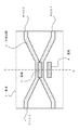
図1は、本発明に係る光スイッチの一実施例を示す平面図である。また、図2は、本発明に係る光スイッチの一実施例を示す断面図である。
図1において半導体の基板30上には、”X字状”の光導波路31が形成される。電極32は、”X字状”の光導波路31の交差部分(光信号を分岐する部分であり、光スイッチ部とも呼ばれる)に形成される。
基板33上にInP層34、下部クラッド層35を結晶成長させる。そして、平坦な下部クラッド層35内で、p側電極40(厳密には、コンタクト層38とp側電極40が接触している部分)の直下以外の部分、すなわち、図2中”DR41”および”DR42”に示す部分にはp型不純物であるZnが選択拡散されて電流狭窄構造を形成する。
光スイッチが”OFF”の場合、電極32(図2中のp側電極40に相当する。)および基板30裏面の図示しないn側電極(図2中のn側電極41に相当する。)には電流が供給されない。
コア層36に量子ドット構造を挿入できるキャリア注入方式の光スイッチには、本発明を適用することができる。例えば、従来例2、3の構成の光スイッチに本発明を適用してもよい。
31 光導波路
35 下部クラッド層
36 コア層
36a n型のInGaAs層
36b InAs量子ドット
37 上部クラッド層
Claims (5)
- 一方から入射された光信号を途中で2つに分岐して出射する光導波路が形成され、前記分岐する部分でキャリア注入によるキャリア濃度変化により屈折率変化を生じさせて光信号の伝送経路を切り換える光スイッチにおいて、
前記光信号が伝搬されるコア層またはこのコア層を含む光導波路層内に量子ドットまたは量子ワイヤを挿入し、
前記入射された光信号は、キャリア注入されていないと前記2つに分岐された光導波路のうち第一の光導波路に出射され、キャリア注入されると第二の光導波路に出射され、
前記量子ドットまたは前記量子ワイヤの大きさは、前記量子ドットまたは前記量子ワイヤでキャリアが消滅するときの発光再結合によって発生する光の波長が、前記光信号の波長と異なるものになるような大きさであって、
前記量子ドットまたは前記量子ワイヤでキャリアが消滅するときの発光再結合によって発生する光を除去する波長選択フィルタを設けたことを特徴とする光スイッチ。 - 光導波路層は、前記光導波路を伝搬する伝搬光が閉じ込められる領域であることを特徴とする請求項1記載の光スイッチ。
- 前記光導波路がスラブ型の光導波路であることを特徴とする請求項1または2記載の光スイッチ。
- 前記光導波路は、2本の直線の光導波路が交差したことを特徴とする請求項1〜3のいずれかに記載の光スイッチ。
- 前記光導波路は、1本の直線の光導波路の途中から異なる角度で分岐する光導波路を有することを特徴とする請求項1〜3のいずれかに記載の光スイッチ。
Priority Applications (2)
| Application Number | Priority Date | Filing Date | Title |
|---|---|---|---|
| JP2004167325A JP4678143B2 (ja) | 2004-06-04 | 2004-06-04 | 光スイッチ |
| US11/144,487 US7200290B2 (en) | 2004-06-04 | 2005-06-02 | Optical switch |
Applications Claiming Priority (1)
| Application Number | Priority Date | Filing Date | Title |
|---|---|---|---|
| JP2004167325A JP4678143B2 (ja) | 2004-06-04 | 2004-06-04 | 光スイッチ |
Publications (2)
| Publication Number | Publication Date |
|---|---|
| JP2005345898A JP2005345898A (ja) | 2005-12-15 |
| JP4678143B2 true JP4678143B2 (ja) | 2011-04-27 |
Family
ID=35498326
Family Applications (1)
| Application Number | Title | Priority Date | Filing Date |
|---|---|---|---|
| JP2004167325A Expired - Fee Related JP4678143B2 (ja) | 2004-06-04 | 2004-06-04 | 光スイッチ |
Country Status (2)
| Country | Link |
|---|---|
| US (1) | US7200290B2 (ja) |
| JP (1) | JP4678143B2 (ja) |
Families Citing this family (4)
| Publication number | Priority date | Publication date | Assignee | Title |
|---|---|---|---|---|
| JP4678143B2 (ja) * | 2004-06-04 | 2011-04-27 | 横河電機株式会社 | 光スイッチ |
| US7989841B1 (en) | 2007-07-31 | 2011-08-02 | Hewlett-Packard Development Company, L.P. | Fast injection optical switch |
| US8131124B2 (en) * | 2008-04-22 | 2012-03-06 | Jamshid Nayyer | Optical guided mode spatial switches and their fabrication |
| WO2025116628A1 (ko) * | 2023-11-29 | 2025-06-05 | 서울대학교산학협력단 | 광도파로가 형성된 기판 및 이를 포함하는 디바이스 |
Family Cites Families (12)
| Publication number | Priority date | Publication date | Assignee | Title |
|---|---|---|---|---|
| JPS6313023A (ja) * | 1986-07-04 | 1988-01-20 | Oki Electric Ind Co Ltd | 導波型光スイツチ |
| JPS6371826A (ja) * | 1986-09-16 | 1988-04-01 | Hitachi Ltd | 光半導体装置 |
| US4987468A (en) * | 1988-06-17 | 1991-01-22 | Xerox Corporation | Lateral heterojunction bipolar transistor (LHBT) and suitability thereof as a hetero transverse junction (HTJ) laser |
| US5422967A (en) * | 1989-01-30 | 1995-06-06 | Hitachi, Ltd. | Self-routing optical switch and optical switch array |
| JPH06130432A (ja) * | 1992-10-19 | 1994-05-13 | Furukawa Electric Co Ltd:The | 光回路 |
| JP3866836B2 (ja) * | 1997-08-14 | 2007-01-10 | 富士通株式会社 | 非線形光学装置 |
| JP3391267B2 (ja) * | 1998-07-14 | 2003-03-31 | 日本電気株式会社 | 全光スイッチ及び波長変換器 |
| US6734453B2 (en) * | 2000-08-08 | 2004-05-11 | Translucent Photonics, Inc. | Devices with optical gain in silicon |
| US6633692B2 (en) * | 2001-07-31 | 2003-10-14 | The National University Of Singapore | High carrier injection optical waveguide switch |
| JP2004029171A (ja) * | 2002-06-24 | 2004-01-29 | Yokogawa Electric Corp | 光スイッチ及びその製造方法 |
| US6836351B2 (en) * | 2002-10-30 | 2004-12-28 | Northrop Grumman Corporation | Quantum-confined stark effect quantum-dot optical modulator |
| JP4678143B2 (ja) * | 2004-06-04 | 2011-04-27 | 横河電機株式会社 | 光スイッチ |
-
2004
- 2004-06-04 JP JP2004167325A patent/JP4678143B2/ja not_active Expired - Fee Related
-
2005
- 2005-06-02 US US11/144,487 patent/US7200290B2/en not_active Expired - Fee Related
Also Published As
| Publication number | Publication date |
|---|---|
| JP2005345898A (ja) | 2005-12-15 |
| US7200290B2 (en) | 2007-04-03 |
| US20060013522A1 (en) | 2006-01-19 |
Similar Documents
| Publication | Publication Date | Title |
|---|---|---|
| US6937781B2 (en) | Optical switch having photonic crystal structure | |
| JP5029369B2 (ja) | 光導波路 | |
| US20090225804A1 (en) | Semiconductor laser and method for manufacturing the same | |
| US5311534A (en) | Semiconductor laser devices | |
| JP4472278B2 (ja) | 半導体レーザ素子 | |
| JPH08220571A (ja) | 小型ディジタル光学スイッチ | |
| JP2000183457A (ja) | 半導体レーザとその製造方法 | |
| JP4011640B2 (ja) | 半導体レーザ,及び半導体レーザの製造方法 | |
| JP2005345898A (ja) | 光スイッチ | |
| JPH07333660A (ja) | 非線形光学素子 | |
| JP2004523120A (ja) | 複数の光学活性領域を備える半導体レーザ | |
| JP2004523117A (ja) | 光学装置のヒートシンク上への取り付け | |
| JP2005266632A (ja) | 光スイッチ | |
| EP2856588B1 (fr) | Laser semiconducteur optimise | |
| JP3255111B2 (ja) | 半導体レーザ及びその製造方法 | |
| US7133577B1 (en) | Optical modulator and methods of making and using optical modulator | |
| US6891986B2 (en) | Optical switch | |
| JPH10117045A (ja) | 光半導体素子 | |
| JP2809216B2 (ja) | 非線形光導波路 | |
| JPS6355878B2 (ja) | ||
| JPH10303499A (ja) | 半導体レーザ及びその製造方法 | |
| JP2841860B2 (ja) | 光半導体装置 | |
| JP4154663B2 (ja) | 光スイッチ | |
| JP2007155967A (ja) | 電磁波偏波面回転装置 | |
| JPH1126874A (ja) | 光半導体素子 |
Legal Events
| Date | Code | Title | Description |
|---|---|---|---|
| A621 | Written request for application examination |
Free format text: JAPANESE INTERMEDIATE CODE: A621 Effective date: 20060407 |
|
| A977 | Report on retrieval |
Free format text: JAPANESE INTERMEDIATE CODE: A971007 Effective date: 20090512 |
|
| A131 | Notification of reasons for refusal |
Free format text: JAPANESE INTERMEDIATE CODE: A131 Effective date: 20090602 |
|
| A521 | Request for written amendment filed |
Free format text: JAPANESE INTERMEDIATE CODE: A523 Effective date: 20090803 |
|
| A131 | Notification of reasons for refusal |
Free format text: JAPANESE INTERMEDIATE CODE: A131 Effective date: 20091002 |
|
| A521 | Request for written amendment filed |
Free format text: JAPANESE INTERMEDIATE CODE: A523 Effective date: 20091201 |
|
| A131 | Notification of reasons for refusal |
Free format text: JAPANESE INTERMEDIATE CODE: A131 Effective date: 20101101 |
|
| A521 | Request for written amendment filed |
Free format text: JAPANESE INTERMEDIATE CODE: A523 Effective date: 20101208 |
|
| TRDD | Decision of grant or rejection written | ||
| A01 | Written decision to grant a patent or to grant a registration (utility model) |
Free format text: JAPANESE INTERMEDIATE CODE: A01 Effective date: 20110105 |
|
| A01 | Written decision to grant a patent or to grant a registration (utility model) |
Free format text: JAPANESE INTERMEDIATE CODE: A01 |
|
| A61 | First payment of annual fees (during grant procedure) |
Free format text: JAPANESE INTERMEDIATE CODE: A61 Effective date: 20110118 |
|
| R150 | Certificate of patent or registration of utility model |
Free format text: JAPANESE INTERMEDIATE CODE: R150 |
|
| FPAY | Renewal fee payment (event date is renewal date of database) |
Free format text: PAYMENT UNTIL: 20140210 Year of fee payment: 3 |
|
| LAPS | Cancellation because of no payment of annual fees |