JP4700636B2 - 半導体メモリ装置を装着したメモリモジュールを有するシステム - Google Patents
半導体メモリ装置を装着したメモリモジュールを有するシステム Download PDFInfo
- Publication number
- JP4700636B2 JP4700636B2 JP2007047258A JP2007047258A JP4700636B2 JP 4700636 B2 JP4700636 B2 JP 4700636B2 JP 2007047258 A JP2007047258 A JP 2007047258A JP 2007047258 A JP2007047258 A JP 2007047258A JP 4700636 B2 JP4700636 B2 JP 4700636B2
- Authority
- JP
- Japan
- Prior art keywords
- clock signal
- signal
- memory module
- address
- command
- Prior art date
- Legal status (The legal status is an assumption and is not a legal conclusion. Google has not performed a legal analysis and makes no representation as to the accuracy of the status listed.)
- Expired - Fee Related
Links
Images


Classifications
-
- G—PHYSICS
- G11—INFORMATION STORAGE
- G11C—STATIC STORES
- G11C7/00—Arrangements for writing information into, or reading information out from, a digital store
- G11C7/10—Input/output [I/O] data interface arrangements, e.g. I/O data control circuits, I/O data buffers
- G11C7/1078—Data input circuits, e.g. write amplifiers, data input buffers, data input registers, data input level conversion circuits
- G11C7/1084—Data input buffers, e.g. comprising level conversion circuits, circuits for adapting load
-
- G—PHYSICS
- G11—INFORMATION STORAGE
- G11C—STATIC STORES
- G11C11/00—Digital stores characterised by the use of particular electric or magnetic storage elements; Storage elements therefor
- G11C11/21—Digital stores characterised by the use of particular electric or magnetic storage elements; Storage elements therefor using electric elements
- G11C11/34—Digital stores characterised by the use of particular electric or magnetic storage elements; Storage elements therefor using electric elements using semiconductor devices
- G11C11/40—Digital stores characterised by the use of particular electric or magnetic storage elements; Storage elements therefor using electric elements using semiconductor devices using transistors
- G11C11/401—Digital stores characterised by the use of particular electric or magnetic storage elements; Storage elements therefor using electric elements using semiconductor devices using transistors forming cells needing refreshing or charge regeneration, i.e. dynamic cells
- G11C11/4063—Auxiliary circuits, e.g. for addressing, decoding, driving, writing, sensing or timing
- G11C11/407—Auxiliary circuits, e.g. for addressing, decoding, driving, writing, sensing or timing for memory cells of the field-effect type
- G11C11/4076—Timing circuits
-
- G—PHYSICS
- G11—INFORMATION STORAGE
- G11C—STATIC STORES
- G11C11/00—Digital stores characterised by the use of particular electric or magnetic storage elements; Storage elements therefor
- G11C11/21—Digital stores characterised by the use of particular electric or magnetic storage elements; Storage elements therefor using electric elements
- G11C11/34—Digital stores characterised by the use of particular electric or magnetic storage elements; Storage elements therefor using electric elements using semiconductor devices
- G11C11/40—Digital stores characterised by the use of particular electric or magnetic storage elements; Storage elements therefor using electric elements using semiconductor devices using transistors
- G11C11/401—Digital stores characterised by the use of particular electric or magnetic storage elements; Storage elements therefor using electric elements using semiconductor devices using transistors forming cells needing refreshing or charge regeneration, i.e. dynamic cells
- G11C11/4063—Auxiliary circuits, e.g. for addressing, decoding, driving, writing, sensing or timing
- G11C11/407—Auxiliary circuits, e.g. for addressing, decoding, driving, writing, sensing or timing for memory cells of the field-effect type
- G11C11/408—Address circuits
- G11C11/4082—Address Buffers; level conversion circuits
-
- G—PHYSICS
- G11—INFORMATION STORAGE
- G11C—STATIC STORES
- G11C11/00—Digital stores characterised by the use of particular electric or magnetic storage elements; Storage elements therefor
- G11C11/21—Digital stores characterised by the use of particular electric or magnetic storage elements; Storage elements therefor using electric elements
- G11C11/34—Digital stores characterised by the use of particular electric or magnetic storage elements; Storage elements therefor using electric elements using semiconductor devices
- G11C11/40—Digital stores characterised by the use of particular electric or magnetic storage elements; Storage elements therefor using electric elements using semiconductor devices using transistors
- G11C11/401—Digital stores characterised by the use of particular electric or magnetic storage elements; Storage elements therefor using electric elements using semiconductor devices using transistors forming cells needing refreshing or charge regeneration, i.e. dynamic cells
- G11C11/4063—Auxiliary circuits, e.g. for addressing, decoding, driving, writing, sensing or timing
- G11C11/407—Auxiliary circuits, e.g. for addressing, decoding, driving, writing, sensing or timing for memory cells of the field-effect type
- G11C11/409—Read-write [R-W] circuits
- G11C11/4093—Input/output [I/O] data interface arrangements, e.g. data buffers
-
- G—PHYSICS
- G11—INFORMATION STORAGE
- G11C—STATIC STORES
- G11C7/00—Arrangements for writing information into, or reading information out from, a digital store
- G11C7/10—Input/output [I/O] data interface arrangements, e.g. I/O data control circuits, I/O data buffers
- G11C7/1072—Input/output [I/O] data interface arrangements, e.g. I/O data control circuits, I/O data buffers for memories with random access ports synchronised on clock signal pulse trains, e.g. synchronous memories, self timed memories
-
- G—PHYSICS
- G11—INFORMATION STORAGE
- G11C—STATIC STORES
- G11C7/00—Arrangements for writing information into, or reading information out from, a digital store
- G11C7/10—Input/output [I/O] data interface arrangements, e.g. I/O data control circuits, I/O data buffers
- G11C7/1078—Data input circuits, e.g. write amplifiers, data input buffers, data input registers, data input level conversion circuits
-
- G—PHYSICS
- G11—INFORMATION STORAGE
- G11C—STATIC STORES
- G11C7/00—Arrangements for writing information into, or reading information out from, a digital store
- G11C7/10—Input/output [I/O] data interface arrangements, e.g. I/O data control circuits, I/O data buffers
- G11C7/1078—Data input circuits, e.g. write amplifiers, data input buffers, data input registers, data input level conversion circuits
- G11C7/109—Control signal input circuits
-
- G—PHYSICS
- G11—INFORMATION STORAGE
- G11C—STATIC STORES
- G11C7/00—Arrangements for writing information into, or reading information out from, a digital store
- G11C7/22—Read-write [R-W] timing or clocking circuits; Read-write [R-W] control signal generators or management
-
- G—PHYSICS
- G11—INFORMATION STORAGE
- G11C—STATIC STORES
- G11C7/00—Arrangements for writing information into, or reading information out from, a digital store
- G11C7/22—Read-write [R-W] timing or clocking circuits; Read-write [R-W] control signal generators or management
- G11C7/222—Clock generating, synchronizing or distributing circuits within memory device
-
- G—PHYSICS
- G11—INFORMATION STORAGE
- G11C—STATIC STORES
- G11C8/00—Arrangements for selecting an address in a digital store
- G11C8/18—Address timing or clocking circuits; Address control signal generation or management, e.g. for row address strobe [RAS] or column address strobe [CAS] signals
Landscapes
- Engineering & Computer Science (AREA)
- Microelectronics & Electronic Packaging (AREA)
- Computer Hardware Design (AREA)
- Dram (AREA)
- Memory System (AREA)
Description
また、メモリコントローラの代りにマイクロプロセッサを具備することを特徴とする。
また、データバッファは、データストローブ信号のエッジごとにデータを入出力することを特徴とする。
また、第1クロック信号、第2クロック信号、アドレス信号及びコマンド信号は、システム内に装着されるメモリコントローラまたはマイクロプロセッサから提供されることを特徴とする。
また、メモリモジュールは、第1クロック信号及び第2クロック信号を受信する2つ以上のモジュールピンを具備することを特徴とする。
また、第1クロック信号、第2クロック信号、アドレス信号及びコマンド信号は、システム内に装着されるメモリコントローラまたはマイクロプロセッサから提供されることを特徴とする。
また、メモリモジュールは、第1クロック信号及び第2クロック信号を受信する2つ以上のモジュールピンを具備することを特徴とする。
また、第1クロック信号、第2クロック信号、アドレス信号及びコマンド信号は、システム内に装着されるメモリコントローラまたはマイクロプロセッサから提供されることを特徴とする。
また、メモリモジュールは、第1クロック信号及び第2クロック信号を受信する2つ以上のモジュールピンを具備することを特徴とする。
また、システムクロック信号、アドレス信号及びコマンド信号は、システム内に装着されるメモリコントローラまたはマイクロプロセッサから提供されることを特徴とする。
また、メモリモジュールは、第1クロック信号及び第2クロック信号を受信する2つ以上のモジュールピンを具備することを特徴とする。
また、システムクロック信号、アドレス信号及びコマンド信号は、システム内に装着されるメモリコントローラまたはマイクロプロセッサから提供されることを特徴とする。
また、メモリモジュールは、第1クロック信号及び第2クロック信号を受信する2つ以上のモジュールピンを具備することを特徴とする。
また、第1クロック信号、第2クロック信号、アドレス信号及びコマンド信号は、システム内に装着されるメモリコントローラまたはマイクロプロセッサから提供されることを特徴とする。
また、メモリモジュールは、第1クロック信号及び第2クロック信号を受信する2つ以上のモジュールピンを具備することを特徴とする。
また、第1クロック信号、第2クロック信号、アドレス信号及びコマンド信号は、システム内に装着されるメモリコントローラまたはマイクロプロセッサから提供されることを特徴とする。
また、メモリモジュールは、第1クロック信号及び第2クロック信号を受信する2つ以上のモジュールピンを具備することを特徴とする。
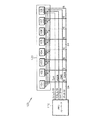
また、本発明のメモリモジュールは、低周波動作のレジスタのために使われる第1クロック信号と高周波動作のメモリチップのために使われる第2クロック信号とを受信する。それで、メモリモジュールが装着されるシステムのクロック周波数が高まっても、メモリモジュール内の動作周波数領域が相異なるレジスタとメモリチップとは該当周波数のクロック信号に選択的に連結されるために安定して動作する。
310 クロックバッファ
320 アドレスバッファ
330 コマンドバッファ
340 データバッファ
350 制御部
Claims (18)
- 第1クロック信号、前記第1クロック信号の周波数より高い周波数の第2クロック信号、アドレス信号及びコマンド信号のバスラインが配置され、これらバスラインと連結されるメモリモジュールを有するシステムにおいて、前記メモリモジュールは、
前記第1クロック信号に連結され、これに応答して前記アドレス信号及び前記コマンド信号を受信し、その出力を前記メモリモジュールの一方向に提供するレジスタと、
前記第2クロック信号に連結され、これに応答して前記レジスタから出力される前記アドレス信号及び前記コマンド信号を受信する多数のメモリチップとを具備することを特徴とするシステム。 - 前記第1クロック信号、前記第2クロック信号、前記アドレス信号及び前記コマンド信号は、
前記システム内に装着されるメモリコントローラまたはマイクロプロセッサから提供されることを特徴とする請求項1に記載のシステム。 - 前記メモリモジュールは、
前記第1クロック信号及び前記第2クロック信号を受信する2つ以上のモジュールピンを具備することを特徴とする請求項1に記載のシステム。 - 第1クロック信号、前記第1クロック信号の周波数より高い周波数の第2クロック信号、アドレス信号及びコマンド信号のバスラインが配置され、これらバスラインと連結されるメモリモジュールを有するシステムにおいて、前記メモリモジュールは、
前記第1クロック信号に連結され、これに応答して前記アドレス信号及び前記コマンド信号を受信し、その出力を前記メモリモジュールの中央で両方向に提供するレジスタと、
前記第2クロック信号に連結され、これに応答して前記レジスタから出力される前記アドレス信号及び前記コマンド信号を受信する多数のメモリチップとを具備することを特徴とするシステム。 - 前記第1クロック信号、前記第2クロック信号、前記アドレス信号及び前記コマンド信号は、
前記システム内に装着されるメモリコントローラまたはマイクロプロセッサから提供されることを特徴とする請求項4に記載のシステム。 - 前記メモリモジュールは、
前記第1クロック信号及び前記第2クロック信号を受信する2つ以上のモジュールピンを具備することを特徴とする請求項4に記載のシステム。 - システムクロック信号、アドレス信号及びコマンド信号のバスラインが配置され、これらバスラインと連結されるメモリモジュールを有するシステムにおいて、
前記システムは、
前記システムクロック信号を受信して第1クロック信号及び前記第1クロック信号の周波数より高い周波数の第2クロック信号を発生させる位相同期回路を具備し、
前記メモリモジュールは前記第1クロック信号に連結され、これに応答して前記アドレス信号及び前記コマンド信号を受信し、その出力を前記メモリモジュールの一方向に提供するレジスタと、
前記第2クロック信号に連結され、これに応答して前記レジスタから出力される前記アドレス信号及び前記コマンド信号を受信する多数のメモリチップとを具備することを特徴とするシステム。 - 前記システムクロック信号、前記アドレス信号及び前記コマンド信号は、
前記システム内に装着されるメモリコントローラまたはマイクロプロセッサから提供されることを特徴とする請求項7に記載のシステム。 - 前記メモリモジュールは、
前記第1クロック信号及び前記第2クロック信号を受信する2つ以上のモジュールピンを具備することを特徴とする請求項7に記載のシステム。 - システムクロック信号、アドレス信号及びコマンド信号のバスラインが配置され、これらバスラインと連結されるメモリモジュールを有するシステムにおいて、
前記システムは、
前記システムクロック信号を受信して第1クロック信号及び前記第1クロック信号の周波数より高い周波数の第2クロック信号を発生させる位相同期回路を具備し、
前記メモリモジュールは、
前記第1クロック信号に連結され、これに応答して前記アドレス信号及び前記コマンド信号を受信し、その出力を前記メモリモジュールの中央で両方向に提供するレジスタと、
前記第2クロック信号に連結され、これに応答して前記レジスタから出力された前記アドレス信号及び前記コマンド信号を受信する多数のメモリチップとを具備することを特徴とするシステム。 - 前記システムクロック信号、前記アドレス信号及び前記コマンド信号は、
前記システム内に装着されるメモリコントローラまたはマイクロプロセッサから提供されることを特徴とする請求項10に記載のシステム。 - 前記メモリモジュールは、
前記第1クロック信号及び前記第2クロック信号を受信する2つ以上のモジュールピンを具備することを特徴とする請求項10に記載のシステム。 - 第1クロック信号、前記第1クロック信号の周波数より高い周波数の第2クロック信号、アドレス信号及びコマンド信号のバスラインが配置され、これらバスラインと連結されるメモリモジュールを有するシステムにおいて、前記メモリモジュールは、
前記第1クロック信号に連結され、これに応答して前記アドレス信号及び前記コマンド信号を受信し、その出力を前記メモリモジュールの一方向に提供するレジスタと、
前記第2クロック信号に連結され、これと位相同期する多数の内部クロック信号を発生させる位相同期回路と、
前記内部クロック信号に各々連結され、これに応答して前記レジスタから出力される前記アドレス信号及び前記コマンド信号を受信する多数のメモリチップとを具備することを特徴とするシステム。 - 前記第1クロック信号、前記第2クロック信号、前記アドレス信号及び前記コマンド信号は、
前記システム内に装着されるメモリコントローラまたはマイクロプロセッサから提供されることを特徴とする請求項13に記載のシステム。 - 前記メモリモジュールは、
前記第1クロック信号及び前記第2クロック信号を受信する2つ以上のモジュールピンを具備することを特徴とする請求項13に記載のシステム。 - 第1クロック信号、前記第1クロック信号の周波数より高い周波数の第2クロック信号、アドレス信号及びコマンド信号のバスラインが配置され、これらバスラインと連結されるメモリモジュールを有するシステムにおいて、前記メモリモジュールは、
前記第1クロック信号に連結され、これに応答して前記アドレス信号及び前記コマンド信号を受信してその出力を前記メモリモジュールの中央で両方向に提供するレジスタと、
前記第2クロック信号に連結され、これと位相同期する多数の内部クロック信号を発生させる位相同期回路と、
前記内部クロック信号に各々連結され、これに応答して前記レジスタから出力される前記アドレス信号及び前記コマンド信号を受信する多数のメモリチップとを具備することを特徴とするシステム。 - 前記第1クロック信号、前記第2クロック信号、前記アドレス信号及び前記コマンド信号は、
前記システム内に装着されるメモリコントローラまたはマイクロプロセッサから提供されることを特徴とする請求項16に記載のシステム。 - 前記メモリモジュールは、
前記第1クロック信号及び前記第2クロック信号を受信する2つ以上のモジュールピンを具備することを特徴とする請求項16に記載のシステム。
Applications Claiming Priority (4)
| Application Number | Priority Date | Filing Date | Title |
|---|---|---|---|
| KR20000052377 | 2000-09-05 | ||
| KR2000P-52377 | 2000-09-05 | ||
| KR2000P-79186 | 2000-12-20 | ||
| KR10-2000-0079186A KR100396885B1 (ko) | 2000-09-05 | 2000-12-20 | 고주파 클럭 신호의 주파수를 낮추어 어드레스 및커맨드의 동작 주파수로 사용하고 서로 다른 주파수의클럭 신호들을 수신하는 반도체 메모리 장치, 이를포함하는 메모리 모듈 및 시스템 메모리 모듈 |
Related Parent Applications (1)
| Application Number | Title | Priority Date | Filing Date |
|---|---|---|---|
| JP2001267266A Division JP3960583B2 (ja) | 2000-09-05 | 2001-09-04 | 半導体メモリ装置及びこれを含むメモリモジュールを有するシステム |
Publications (2)
| Publication Number | Publication Date |
|---|---|
| JP2007200542A JP2007200542A (ja) | 2007-08-09 |
| JP4700636B2 true JP4700636B2 (ja) | 2011-06-15 |
Family
ID=26638371
Family Applications (2)
| Application Number | Title | Priority Date | Filing Date |
|---|---|---|---|
| JP2001267266A Expired - Fee Related JP3960583B2 (ja) | 2000-09-05 | 2001-09-04 | 半導体メモリ装置及びこれを含むメモリモジュールを有するシステム |
| JP2007047258A Expired - Fee Related JP4700636B2 (ja) | 2000-09-05 | 2007-02-27 | 半導体メモリ装置を装着したメモリモジュールを有するシステム |
Family Applications Before (1)
| Application Number | Title | Priority Date | Filing Date |
|---|---|---|---|
| JP2001267266A Expired - Fee Related JP3960583B2 (ja) | 2000-09-05 | 2001-09-04 | 半導体メモリ装置及びこれを含むメモリモジュールを有するシステム |
Country Status (6)
| Country | Link |
|---|---|
| US (1) | US6496445B2 (ja) |
| JP (2) | JP3960583B2 (ja) |
| CN (1) | CN1343987B (ja) |
| DE (1) | DE10144247B4 (ja) |
| GB (1) | GB2370667B (ja) |
| TW (1) | TW530207B (ja) |
Families Citing this family (41)
| Publication number | Priority date | Publication date | Assignee | Title |
|---|---|---|---|---|
| JP4139579B2 (ja) * | 2001-06-19 | 2008-08-27 | 株式会社ルネサステクノロジ | 半導体装置および半導体装置の動作モード制御方法 |
| US6918078B2 (en) * | 2001-07-23 | 2005-07-12 | Intel Corporation | Systems with modules sharing terminations |
| US6724082B2 (en) * | 2001-07-23 | 2004-04-20 | Intel Corporation | Systems having modules with selectable on die terminations |
| US6711027B2 (en) * | 2001-07-23 | 2004-03-23 | Intel Corporation | Modules having paths of different impedances |
| US6631083B2 (en) * | 2001-07-23 | 2003-10-07 | Intel Corporation | Systems with modules and clocking therefore |
| US6771515B2 (en) * | 2001-07-23 | 2004-08-03 | Intel Corporation | Systems having modules with on die terminations |
| US6717823B2 (en) * | 2001-07-23 | 2004-04-06 | Intel Corporation | Systems having modules with buffer chips |
| US6674649B2 (en) * | 2001-07-23 | 2004-01-06 | Intel Corporation | Systems having modules sharing on module terminations |
| US6674648B2 (en) * | 2001-07-23 | 2004-01-06 | Intel Corporation | Termination cards and systems therefore |
| JP4812976B2 (ja) * | 2001-07-30 | 2011-11-09 | エルピーダメモリ株式会社 | レジスタ、メモリモジュール及びメモリシステム |
| US6944738B2 (en) * | 2002-04-16 | 2005-09-13 | Sun Microsystems, Inc. | Scalable design for DDR SDRAM buses |
| JP3838939B2 (ja) | 2002-05-22 | 2006-10-25 | エルピーダメモリ株式会社 | メモリシステムとモジュール及びレジスタ |
| US6650594B1 (en) * | 2002-07-12 | 2003-11-18 | Samsung Electronics Co., Ltd. | Device and method for selecting power down exit |
| US6930953B2 (en) * | 2002-09-16 | 2005-08-16 | Texas Instruments Incorporated | Self-timed strobe generator and method for use with multi-strobe random access memories to increase memory bandwidth |
| KR100513372B1 (ko) * | 2003-05-24 | 2005-09-06 | 주식회사 하이닉스반도체 | 명령 및 어드레스 버스에 사용되는 클럭 신호의 주파수와데이터 버스에 대해 사용되는 클럭 신호의 주파수를다르게 설정하는 서브 시스템 |
| KR100546362B1 (ko) * | 2003-08-12 | 2006-01-26 | 삼성전자주식회사 | 메모리 클럭 신호의 주파수를 선택적으로 가변시키는메모리 컨트롤러 및 이를 이용한 메모리의 데이터 독출동작 제어방법 |
| KR100539252B1 (ko) * | 2004-03-08 | 2005-12-27 | 삼성전자주식회사 | 데이터 버스 및 커맨드/어드레스 버스를 통해 전송되는신호의 충실도를 향상시킬 수 있는 메모리 모듈 및 이를포함하는 메모리 시스템 |
| KR100551475B1 (ko) * | 2004-08-31 | 2006-02-14 | 삼성전자주식회사 | 비주기 클록옵션을 가지는 메모리 모듈과 모듈용 메모리칩 및 허브 칩 |
| US7188208B2 (en) * | 2004-09-07 | 2007-03-06 | Intel Corporation | Side-by-side inverted memory address and command buses |
| KR100568546B1 (ko) | 2004-10-19 | 2006-04-07 | 삼성전자주식회사 | 메모리 시스템, 반도체 메모리 장치, 및 이 시스템과장치의 출력 데이터 스트로우브 신호 발생 방법 |
| KR100562655B1 (ko) * | 2005-02-28 | 2006-03-20 | 주식회사 하이닉스반도체 | 반도체 기억 소자의 동작 제한 필터 및 그 방법 |
| US7339840B2 (en) * | 2005-05-13 | 2008-03-04 | Infineon Technologies Ag | Memory system and method of accessing memory chips of a memory system |
| KR100812600B1 (ko) * | 2005-09-29 | 2008-03-13 | 주식회사 하이닉스반도체 | 주파수가 다른 복수의 클럭을 사용하는 반도체메모리소자 |
| US7747833B2 (en) | 2005-09-30 | 2010-06-29 | Mosaid Technologies Incorporated | Independent link and bank selection |
| US7652922B2 (en) | 2005-09-30 | 2010-01-26 | Mosaid Technologies Incorporated | Multiple independent serial link memory |
| KR101260632B1 (ko) | 2005-09-30 | 2013-05-03 | 모사이드 테크놀로지스 인코퍼레이티드 | 출력 제어 메모리 |
| US20070076502A1 (en) | 2005-09-30 | 2007-04-05 | Pyeon Hong B | Daisy chain cascading devices |
| TWI386846B (zh) * | 2006-03-30 | 2013-02-21 | Silicon Image Inc | 利用共享式非揮發性記憶體初始化多個處理元件之方法、系統及快閃記憶體元件 |
| KR100974222B1 (ko) | 2008-11-13 | 2010-08-06 | 주식회사 하이닉스반도체 | 반도체 메모리 장치 |
| US20100169698A1 (en) * | 2008-12-25 | 2010-07-01 | Kabushiki Kaisha Toshiba | Recording medium control element, recording medium control circuit board, and recording medium control device |
| CN101923524B (zh) * | 2010-08-04 | 2012-08-22 | 苏州国芯科技有限公司 | 一种基于clb总线的存储器接口方法 |
| KR20130000241A (ko) * | 2011-06-22 | 2013-01-02 | 에스케이하이닉스 주식회사 | 칩 선택 회로 및 이를 포함하는 반도체 장치 |
| KR102190962B1 (ko) | 2013-12-30 | 2020-12-14 | 삼성전자주식회사 | 코맨드 처리 회로 및 이를 포함하는 메모리 장치 |
| CN103714012B (zh) * | 2013-12-30 | 2016-08-17 | 龙芯中科技术有限公司 | 数据处理方法和装置 |
| KR102420152B1 (ko) | 2015-11-18 | 2022-07-13 | 삼성전자주식회사 | 메모리 시스템에서의 다중 통신 장치 |
| KR102641515B1 (ko) * | 2016-09-19 | 2024-02-28 | 삼성전자주식회사 | 메모리 장치 및 그것의 클록 분배 방법 |
| US10437514B2 (en) * | 2017-10-02 | 2019-10-08 | Micron Technology, Inc. | Apparatuses and methods including memory commands for semiconductor memories |
| US10467158B2 (en) | 2017-11-29 | 2019-11-05 | Micron Technology, Inc. | Apparatuses and methods including memory commands for semiconductor memories |
| US11132307B2 (en) | 2018-05-25 | 2021-09-28 | Rambus Inc. | Low latency memory access |
| CN111128258B (zh) * | 2018-10-30 | 2024-09-27 | 长鑫存储技术有限公司 | 电源调节电路及方法、存储器 |
| US11967363B2 (en) * | 2020-11-25 | 2024-04-23 | Ap Memory Technology Corporation | Display controller having a surge protection unit and display system thereof |
Family Cites Families (16)
| Publication number | Priority date | Publication date | Assignee | Title |
|---|---|---|---|---|
| CA1243138A (en) * | 1984-03-09 | 1988-10-11 | Masahiro Kodama | High speed memory access circuit of crt display unit |
| JP3476231B2 (ja) * | 1993-01-29 | 2003-12-10 | 三菱電機エンジニアリング株式会社 | 同期型半導体記憶装置および半導体記憶装置 |
| JP2742220B2 (ja) * | 1994-09-09 | 1998-04-22 | 松下電器産業株式会社 | 半導体記憶装置 |
| JP3986578B2 (ja) * | 1996-01-17 | 2007-10-03 | 三菱電機株式会社 | 同期型半導体記憶装置 |
| JPH1011966A (ja) * | 1996-06-27 | 1998-01-16 | Mitsubishi Electric Corp | 同期型半導体記憶装置および同期型メモリモジュール |
| EP0929075B1 (en) * | 1996-09-26 | 2003-08-20 | Mitsubishi Denki Kabushiki Kaisha | Synchronous type semiconductor memory device |
| US5933379A (en) * | 1996-11-18 | 1999-08-03 | Samsung Electronics, Co., Ltd. | Method and circuit for testing a semiconductor memory device operating at high frequency |
| JPH10334659A (ja) | 1997-05-29 | 1998-12-18 | Mitsubishi Electric Corp | 同期型半導体記憶装置 |
| US5978284A (en) * | 1997-08-22 | 1999-11-02 | Micron Technology, Inc. | Synchronous memory with programmable read latency |
| KR100252048B1 (ko) * | 1997-11-18 | 2000-05-01 | 윤종용 | 반도체 메모리장치의 데이터 마스킹 회로 및 데이터 마스킹방법 |
| KR100265610B1 (ko) * | 1997-12-31 | 2000-10-02 | 김영환 | 데이터 전송속도를 증가시킨 더블 데이터 레이트 싱크로너스 디램 |
| JPH11213666A (ja) | 1998-01-30 | 1999-08-06 | Mitsubishi Electric Corp | 出力回路および同期型半導体記憶装置 |
| AU3344999A (en) * | 1998-04-21 | 1999-11-08 | Matsushita Electric Industrial Co., Ltd. | Semiconductor storage device |
| JP4043151B2 (ja) | 1998-08-26 | 2008-02-06 | 富士通株式会社 | 高速ランダムアクセス可能なメモリデバイス |
| KR100301046B1 (ko) * | 1998-09-01 | 2001-09-06 | 윤종용 | 그래픽처리속도를향상시킬수있는듀얼포트를갖는고속싱크로너스메모리장치 |
| US6807613B1 (en) * | 2000-08-21 | 2004-10-19 | Mircon Technology, Inc. | Synchronized write data on a high speed memory bus |
-
2001
- 2001-08-22 GB GB0120457A patent/GB2370667B/en not_active Expired - Fee Related
- 2001-08-22 TW TW090120621A patent/TW530207B/zh not_active IP Right Cessation
- 2001-08-30 CN CN01125164.6A patent/CN1343987B/zh not_active Expired - Fee Related
- 2001-09-04 JP JP2001267266A patent/JP3960583B2/ja not_active Expired - Fee Related
- 2001-09-05 US US09/946,166 patent/US6496445B2/en not_active Expired - Fee Related
- 2001-09-05 DE DE10144247A patent/DE10144247B4/de not_active Expired - Fee Related
-
2007
- 2007-02-27 JP JP2007047258A patent/JP4700636B2/ja not_active Expired - Fee Related
Also Published As
| Publication number | Publication date |
|---|---|
| JP2002133867A (ja) | 2002-05-10 |
| DE10144247B4 (de) | 2013-11-14 |
| GB2370667B (en) | 2003-02-12 |
| DE10144247A1 (de) | 2002-03-14 |
| GB0120457D0 (en) | 2001-10-17 |
| CN1343987A (zh) | 2002-04-10 |
| US20020039324A1 (en) | 2002-04-04 |
| CN1343987B (zh) | 2010-05-05 |
| TW530207B (en) | 2003-05-01 |
| JP3960583B2 (ja) | 2007-08-15 |
| JP2007200542A (ja) | 2007-08-09 |
| GB2370667A (en) | 2002-07-03 |
| US6496445B2 (en) | 2002-12-17 |
Similar Documents
| Publication | Publication Date | Title |
|---|---|---|
| JP4700636B2 (ja) | 半導体メモリ装置を装着したメモリモジュールを有するシステム | |
| US6611905B1 (en) | Memory interface with programable clock to output time based on wide range of receiver loads | |
| US7605631B2 (en) | Delay line synchronizer apparatus and method | |
| US6446158B1 (en) | Memory system using FET switches to select memory banks | |
| JP4561782B2 (ja) | 半導体メモリ装置、半導体メモリ装置の動作方法 | |
| KR100626375B1 (ko) | 고주파로 동작하는 반도체 메모리 장치 및 모듈 | |
| US20040133758A1 (en) | Memory controller, interface device and method using a mode selection signal to support different types of memories | |
| KR20030033070A (ko) | 버퍼가 장착된 메모리 시스템에서 신뢰성있는 전송을제공하기 위한 시스템 및 방법 | |
| US7158443B2 (en) | Delay-lock loop and method adapting itself to operate over a wide frequency range | |
| JP2000187522A (ja) | Ddrタイミングのためのデ―タクロック待ち時間補償回路及び方法 | |
| KR20050104235A (ko) | 메모리 장치용 입력 회로 | |
| KR100883140B1 (ko) | 데이터 출력 제어회로, 반도체 메모리 장치 및 그의 동작방법 | |
| CN117437946A (zh) | 用于提供活动及非活动时钟信号的设备及方法 | |
| JP4561783B2 (ja) | 半導体メモリ装置、半導体メモリ装置の動作方法 | |
| US20090097329A1 (en) | Semiconductor storage device and high-speed address-latching method | |
| KR100560644B1 (ko) | 클럭 동기회로를 구비하는 집적회로장치 | |
| KR100396885B1 (ko) | 고주파 클럭 신호의 주파수를 낮추어 어드레스 및커맨드의 동작 주파수로 사용하고 서로 다른 주파수의클럭 신호들을 수신하는 반도체 메모리 장치, 이를포함하는 메모리 모듈 및 시스템 메모리 모듈 | |
| US5926837A (en) | Memory system capable of reducing timing skew between clock signal and data | |
| US7366827B2 (en) | Method and apparatus for selectively transmitting command signal and address signal | |
| KR100360409B1 (ko) | 명령 및 어드레스 전용 스트로브 신호를 이용하는 반도체메모리장치 및 이의 명령 및 어드레스 입력방법 | |
| US7791963B2 (en) | Semiconductor memory device and operation method thereof | |
| TWI238934B (en) | Memory system using non-distributed command/address clock | |
| JP3173728B2 (ja) | 半導体装置 | |
| JP2007164599A (ja) | メモリモジュール | |
| JP2008305349A (ja) | メモリコントローラ |
Legal Events
| Date | Code | Title | Description |
|---|---|---|---|
| A977 | Report on retrieval |
Free format text: JAPANESE INTERMEDIATE CODE: A971007 Effective date: 20100430 |
|
| A131 | Notification of reasons for refusal |
Free format text: JAPANESE INTERMEDIATE CODE: A131 Effective date: 20100518 |
|
| A521 | Request for written amendment filed |
Free format text: JAPANESE INTERMEDIATE CODE: A523 Effective date: 20100729 |
|
| A01 | Written decision to grant a patent or to grant a registration (utility model) |
Free format text: JAPANESE INTERMEDIATE CODE: A01 Effective date: 20110208 |
|
| A61 | First payment of annual fees (during grant procedure) |
Free format text: JAPANESE INTERMEDIATE CODE: A61 Effective date: 20110304 |
|
| LAPS | Cancellation because of no payment of annual fees |