JP4714876B2 - antenna - Google Patents
antenna Download PDFInfo
- Publication number
- JP4714876B2 JP4714876B2 JP2006218503A JP2006218503A JP4714876B2 JP 4714876 B2 JP4714876 B2 JP 4714876B2 JP 2006218503 A JP2006218503 A JP 2006218503A JP 2006218503 A JP2006218503 A JP 2006218503A JP 4714876 B2 JP4714876 B2 JP 4714876B2
- Authority
- JP
- Japan
- Prior art keywords
- antenna
- ground plane
- elements
- parasitic
- shape
- Prior art date
- Legal status (The legal status is an assumption and is not a legal conclusion. Google has not performed a legal analysis and makes no representation as to the accuracy of the status listed.)
- Expired - Fee Related
Links
Images




Landscapes
- Variable-Direction Aerials And Aerial Arrays (AREA)
- Details Of Aerials (AREA)
Description
本発明は、垂直偏波の送受信が可能で、小型にするのに好適なアンテナに関する。 The present invention relates to an antenna that can transmit and receive vertically polarized waves and is suitable for miniaturization.
従来から、電子走査導波器アレーアンテナの技術が提案されている。このようなアンテナについては、以下の文献に開示がされている。
[非特許文献1]では、1つの給電素子と複数の無給電素子から構成されるアンテナが提案されている。無給電素子には安価なバラクタが装荷され、そのリアクタンス値を変えることにより、指向性を制御するものである。 [Non-Patent Document 1] proposes an antenna including one feeding element and a plurality of parasitic elements. The parasitic element is loaded with an inexpensive varactor, and its directivity is controlled by changing its reactance value.
バラクタのリアクタンス可変範囲は通信周波数に反比例して大きくなるので、低周波数帯では高い指向性可変能力が得られる。無給電素子はアンテナ素子間相互結合により励振されるため、アンテナ素子の間隔を狭めることができる。 Since the variable range of the reactance of the varactor increases in inverse proportion to the communication frequency, a high directivity variable capability can be obtained in the low frequency band. Since the parasitic elements are excited by mutual coupling between the antenna elements, the distance between the antenna elements can be reduced.
[非特許文献2]では、本技術を踏まえて、アンテナ素子半径を約0.05波長に狭め、アンテナ素子間隔を約0.25波長とし、配列スペースを従来型アンテナの約4%程度に小さくする技術を提案している。 In [Non-patent Document 2], based on this technology, the antenna element radius is reduced to about 0.05 wavelength, the antenna element interval is set to about 0.25 wavelength, and the arrangement space is reduced to about 4% of the conventional antenna. The technology to do is proposed.
これらの技術においては、アンテナ素子として用いられるモノポールの長さは約0.25波長であり、地板に垂直に配置されるため、アンテナ全体高さが高くなってしまう。そこで、[非特許文献3]では、アンテナ素子の低姿勢化を図るため、ループに2つのバラクタを逆直列に装荷する技術を提案している。 In these techniques, the length of a monopole used as an antenna element is about 0.25 wavelength, and is disposed perpendicular to the ground plane, so that the overall height of the antenna is increased. [Non-Patent Document 3] proposes a technique of loading two varactors in anti-series in a loop in order to reduce the posture of the antenna element.
本技術では、印加する直流(DC;direct current)電圧の向きを変更すれば2つの可変リアクタの電気容量値が交換され、指向性を2方向に切り換えることができる。この直流電圧は、RF(Radio Frequency)給電線を利用して制御することもできる。そして、ループ径は、約8分の1波長となるので、小型化を図ることも可能である。 In the present technology, if the direction of a direct current (DC) voltage to be applied is changed, the capacitance values of the two variable reactors are exchanged, and the directivity can be switched between two directions. This DC voltage can also be controlled using an RF (Radio Frequency) feeder line. Since the loop diameter is about one-eighth wavelength, it is possible to reduce the size.
しかしながら、[非特許文献1][非特許文献2]の電子走査導波器アレーアンテナでは、垂直偏波の送受信が可能であるが、[非特許文献3]のアンテナは、水平偏波となってしまう。 However, the electronic scanning waveguide array antennas of [Non-Patent Document 1] and [Non-Patent Document 2] can transmit and receive vertically polarized waves, but the antenna of [Non-Patent Document 3] has horizontally polarized waves. End up.
したがって、垂直偏波の送受信が可能なアンテナの低姿勢化を可能とする技術が強く求められている。 Therefore, there is a strong demand for a technique that enables a low-profile antenna that can transmit and receive vertically polarized waves.
本発明は、上記の課題を解決しようとするものであって、垂直偏波の送受信が可能で、小型にするのに好適なアンテナを提供することを目的とする。 An object of the present invention is to provide an antenna that can transmit and receive vertically polarized waves and is suitable for miniaturization.
以上の目的を達成するため、本発明の原理にしたがって、下記の発明を開示する。 In order to achieve the above object, the following invention is disclosed in accordance with the principle of the present invention.
本発明の第1の観点に係るアンテナは、地板、3つのアンテナ素子、2つのバラクタ、信号端子を備え、以下のように構成する。 An antenna according to a first aspect of the present invention includes a ground plane, three antenna elements, two varactors, and a signal terminal, and is configured as follows.
ここで、地板は、略平面形状を有し、導電性である。 Here, the ground plane has a substantially planar shape and is conductive.
一方、3つのアンテナ素子は、地板に平行な棒形状を有し、等間隔に平行に配置される。 On the other hand, the three antenna elements have a bar shape parallel to the ground plane and are arranged in parallel at equal intervals.
さらに、2つのバラクタは、3つのアンテナ素子のうち中央のアンテナ素子である給電素子の先端と、当該給電素子以外の2つのアンテナ素子である無給電素子の先端のそれぞれと、を、接続する。 Further, the two varactors connect the tip of the feeding element, which is the central antenna element among the three antenna elements, to each of the tips of the parasitic elements, which are two antenna elements other than the feeding element.
そして、信号端子は、地板と、当該給電素子の後端と、の間の電位差の変化により信号を伝達する。 And a signal terminal transmits a signal by the change of the electrical potential difference between a ground plane and the rear end of the said electric power feeding element.
また、本発明のアンテナは、2つの容量素子、電圧印加部をさらに備え、以下のように構成することができる。 The antenna of the present invention further includes two capacitive elements and a voltage application unit, and can be configured as follows.
すなわち、2つの容量素子は、地板と、当該2つの無給電素子の後端のそれぞれと、の間に接続される。 That is, the two capacitive elements are connected between the ground plane and each of the rear ends of the two parasitic elements.
一方、電圧印加部は、当該2つの無給電素子の後端の間に直流電圧を印加する。 On the other hand, the voltage application unit applies a DC voltage between the rear ends of the two parasitic elements.
さらに、2つのバラクタは、逆方向に接続される。 Furthermore, the two varactors are connected in opposite directions.
また、本発明のアンテナにおいて、地板と、当該2つの無給電素子の後端のそれぞれとは、接続され、2つのバラクタは、順方向に接続されるように構成することができる。 In the antenna of the present invention, the ground plane and each of the rear ends of the two parasitic elements can be connected, and the two varactors can be connected in the forward direction.
また、本発明のアンテナにおいて、3つのアンテナ素子は、L字型の形状を有し、当該L字型の長辺は、地板と平行な棒形状を有し、当該L字型の短辺は、地板に垂直な棒形状を有するように構成することができる。 In the antenna of the present invention, the three antenna elements have an L-shape, the long sides of the L-shape have a bar shape parallel to the ground plane, and the short sides of the L-shape are It can be configured to have a bar shape perpendicular to the ground plane.
また、本発明のアンテナは、3つのアンテナ素子と、地板と、の間を充填する誘電体をさらに備えるように構成することができる。 In addition, the antenna of the present invention can be configured to further include a dielectric filling the space between the three antenna elements and the ground plane.
また、本発明のアンテナにおいて、地板は、プリント基板の片面に配置される導電性箔であり、3つのアンテナ素子は、当該プリント基板の反対面に配置される導電性箔であり、3つのアンテナ素子のそれぞれの後端は、当該プリント基板のスルーホールを通過して接続されるように構成することができる。 In the antenna of the present invention, the ground plane is a conductive foil disposed on one side of the printed circuit board, and the three antenna elements are conductive foils disposed on the opposite surface of the printed circuit board. Each rear end of the element can be configured to be connected through a through hole of the printed circuit board.
また、本発明のアンテナにおいて、当該給電素子の長さを、当該無給電素子の長さと異なるものとして、所望のリアクタンス可変幅における動作利得を最大化するように構成することができる。 In the antenna according to the present invention, the length of the feeding element may be different from the length of the parasitic element so as to maximize the operation gain in a desired reactance variable width.
また、本発明のアンテナにおいて、当該給電素子にインダクタもしくはコンデンサを接続して、所望のリアクタンス可変幅における動作利得を最大化するように構成することができる。 In the antenna of the present invention, an inductor or a capacitor can be connected to the feed element so as to maximize the operating gain in a desired reactance variable width.
また、本発明のアンテナにおいて、3つのアンテナ素子同士の間隔は、通信に用いる波長の0.04倍であり、3つのアンテナ素子の長さは、当該波長の0.195倍であり、3つのアンテナ素子と地板との間隔は、当該波長の0.045倍であり、3つのアンテナ素子の直径は、当該波長の0.012倍であるように構成することができる。 In the antenna of the present invention, the distance between the three antenna elements is 0.04 times the wavelength used for communication, and the length of the three antenna elements is 0.195 times the wavelength. The distance between the antenna element and the ground plane is 0.045 times the wavelength, and the diameters of the three antenna elements can be configured to be 0.012 times the wavelength.
本発明によれば、垂直偏波の送受信が可能で、小型にするのに好適なアンテナを提供することができる。 According to the present invention, it is possible to provide an antenna that can transmit and receive vertically polarized waves and is suitable for miniaturization.
以下に本発明の一実施形態を説明する。なお、以下に説明する実施形態は説明のためのものであり、本発明の範囲を制限するものではない。したがって、当業者であればこれらの各要素もしくは全要素をこれと均等なものに置換した実施形態を採用することが可能であるが、これらの実施形態も本発明の範囲に含まれる。 An embodiment of the present invention will be described below. In addition, embodiment described below is for description and does not limit the scope of the present invention. Therefore, those skilled in the art can employ embodiments in which each or all of these elements are replaced with equivalent ones, and these embodiments are also included in the scope of the present invention.
図1および図2は、本実施形態に係るアンテナの概要構成を示す説明図である。以下、これらの図を参照して説明する。 1 and 2 are explanatory diagrams showing a schematic configuration of the antenna according to the present embodiment. Hereinafter, description will be given with reference to these drawings.
アンテナ101は、1つの給電素子102と、これを挟むように平行に配置されている2つの無給電素子103と、地板104と、信号端子105と、2つのバラクタ(可変容量ダイオードあるいはバリキャップと呼ばれることもある。)106とからなる。
The
給電素子102および無給電素子103の概形は、いずれも同型のL字形で、等間隔に配置されている。L字形の短辺は、地板104にほぼ垂直であり、L字形の長辺は、地板104にほぼ平行である。
The general shapes of the
無給電素子103のそれぞれの先端と、給電素子102の先端と、は、いずれもバラクタ106で接続されている。
Each tip of the
また、無給電素子103のそれぞれの後端と、給電素子102の後端と、は、地板104に固定されている。無給電素子103の後端と地板104とが電気的に接続される態様は、バラクタ106が順方向に接続されているか逆方向に接続されているかによって異なる。
Further, the rear end of each
信号端子105は、地板104と給電素子102の後端との間の電位差により、信号を伝達するためのもので、典型的には同軸ケーブル108等を経由してRF信号通信機109等に接続される。
The
これらの図に示す例では、給電素子102、無給電素子103、バラクタ106の概形は、いずれも同じ太さの細長い円柱(丸線)状の形状をしている。したがって、これらを全体で見ると、熊手型、あるいは、E字形の形状をしていることになる。
In the examples shown in these drawings, the outlines of the
本図では、理解を容易にするため、信号端子105を給電素子102の後端と地板104における給電素子102の後端近傍付近から延長した導線の先に配置しているが、その位置は任意であり、たとえば地板104の裏側に直接信号端子105を配置することもできる。
In this figure, for the sake of easy understanding, the
これらの形状は、同じ断面形状の角柱状としたり、導体箔とこれに接続される任意の大きさの電子素子とすることも可能である。これらの実施形態については後述する。 These shapes may be prismatic shapes having the same cross-sectional shape, or may be a conductor foil and an electronic element of any size connected to the conductor foil. These embodiments will be described later.
図1に示す実施例は、バラクタ106が逆方向に接続されている態様であり、この場合は、無給電素子103の後端と、地板104とは、コンデンサ110を介して接続される。
The embodiment shown in FIG. 1 is a mode in which the
本図では、理解を容易にするため、コンデンサ110と地板104との距離が離れているように図示しているが、実際には両者がもっと近接するように配置するのが典型的である。
In this figure, in order to facilitate understanding, the
なお、近接対向する導体はコンデンサとして機能するので、設計によっては、明示的にコンデンサ110を用意しなくとも良い。無給電素子103の後端と、地板104との間にこれと等価な容量を配置したのと同等の機能を果たすことができるからである。
In addition, since the conductors that face each other function as a capacitor, the
また、無給電素子103の後端同士には、電圧印加部111と抵抗112により、直流電圧が印加される。
A DC voltage is applied to the rear ends of the
図2に示す実施例は、バラクタ106が順方向に接続されている態様であり、この場合は、無給電素子103の後端は、地板104に直接接続される。
The embodiment shown in FIG. 2 is a mode in which the
この場合は、同軸ケーブル108の軸線(給電素子102に接続されている線)とRF信号通信機109との間にコンデンサ110が接続されるとともに、同軸ケーブル108の軸線と同軸ケーブル108の被覆(地板104に接続されている被覆)との間は、電圧印加部111と抵抗112が直列に接続されている。
In this case, the
図3、図4、図5は、これらのアンテナの等価回路を示す回路図である。以下、これらの図を参照して説明する。 3, 4 and 5 are circuit diagrams showing equivalent circuits of these antennas. Hereinafter, description will be given with reference to these drawings.
これらの図においては、図1、図2において図示を省略していた抵抗やコンデンサ、バラクタなどの要素を付加するとともに、さらに、回路の形状から自然に構成される仮想的な等価電子素子についても図示している。また、本願では、「○○≫××」との表記で、「○○は××より十分に大きい」との意味を表すものとし、「○○≫1」との表記で、「○○は十分に大きい値を有する」との意味を表すものとする。 In these figures, elements such as resistors, capacitors, and varactors that are not shown in FIGS. 1 and 2 are added, and further, virtual equivalent electronic elements that are naturally formed from the shape of the circuit are also included. It is shown. Further, in the present application, the notation “XX >> XX” represents the meaning of “XX is sufficiently larger than XX”, and the notation “XX >> 1” indicates “XX”. "Has a sufficiently large value".
図3には、図1に示すアンテナの等価回路の回路図を示す。本図では、信号端子106から先の同軸ケーブル108およびRF信号通信機109は図示を省略している。
FIG. 3 shows a circuit diagram of an equivalent circuit of the antenna shown in FIG. In this figure, the
バラクタ106(容量Cxmax,Cxmin)は逆方向に接続されており、無給電素子103と地板104との間のコンデンサ110(容量C≫1)は、直流電流をカットするために挿入されている。
The varactor 106 (capacitance Cx max , Cx min ) is connected in the opposite direction, and a capacitor 110 (capacitance C >> 1) between the
また、電圧印加部111(電圧VDC)は、信号端子105を介して接続されるRF信号通信機109に基づくRF信号をカットするために、抵抗112(抵抗値R≫1)を介して接続される。
The voltage application unit 111 (voltage V DC ) is connected via a resistor 112 (resistance value R >> 1) in order to cut an RF signal based on the RF
この態様では、電圧印加部111により印加される電圧VDCの向きによって、バラクタ106のそれぞれの容量を変化させる。
In this aspect, the capacitance of each
図4には、図2に示すアンテナの等価回路の回路図の一例を示す。 FIG. 4 shows an example of a circuit diagram of an equivalent circuit of the antenna shown in FIG.
バラクタ106(容量Cxmax,Cxmin)は順方向に接続されている。 The varactors 106 (capacitances Cx max , Cx min ) are connected in the forward direction.
コンデンサ110の両端は、抵抗113(抵抗値R'≫1)で接続されており、無給電素子103と地板104との間のコンデンサ110(容量C≫1)は、直流電流をカットするために挿入されている。
Both ends of the
また、電圧印加部111(電圧VDC)は、信号端子105を介して接続されるRF信号通信機109に基づくRF信号をカットするために、抵抗112(抵抗値R≫1)を介して接続される。
The voltage application unit 111 (voltage V DC ) is connected via a resistor 112 (resistance value R >> 1) in order to cut an RF signal based on the RF
この態様では、電圧印加部111により印加される電圧VDCの向きによって、バラクタ106のそれぞれの容量を変化させる。また、電圧印加部111(電圧VDC)は、信号端子105を介して接続することが可能となる。
In this aspect, the capacitance of each
バラクタ106は、印加される直流電圧に対して並列接続となるため、それぞれにコンデンサ114(容量C'≫Cxmax)と抵抗113(抵抗値R'≫1)を接続するほか、コンデンサ110(容量C≫1)および抵抗115(抵抗値R''≫1)を用いて直流電流をカットする。
Since the
また、電圧印加部111(電圧VDC)は、信号端子105を介して接続されるRF信号通信機109に基づくRF信号をカットするために、抵抗112(抵抗値R≫1)を介して接続される。
The voltage application unit 111 (voltage V DC ) is connected via a resistor 112 (resistance value R >> 1) in order to cut an RF signal based on the RF
図5には、図2に示すアンテナの等価回路の回路図(図4に示したもの)の変形例を示す。本実施形態では、コンデンサ114(容量C'≫Cxmax)とのかわりに、逆向きにバラクタ116(容量Cx'min,Cx'max、ただしCx'min≫Cxmax)を接続している。 FIG. 5 shows a modification of the circuit diagram (shown in FIG. 4) of the equivalent circuit of the antenna shown in FIG. In the present embodiment, are connected in place of the capacitor 114 (capacitance C'»Cx max), the varactor in the opposite direction 116 (capacitance Cx 'min, Cx' max, but Cx 'min »Cx max) a.
コンデンサ114(容量C'≫Cxmax)やバラクタ116(容量Cx'min,Cx'max)は、直流電流をカットするために利用するので、大きな電気容量のものを利用すれば、RF信号周波数においては、ほぼ短絡状態にすることができる。したがって、これらのコンデンサ114やバラクタ116を配置する場所は、アンテナ101の上面など、任意の場所とすることができる。
Since the capacitor 114 (capacitance C ′ >> Cx max ) and the varactor 116 (capacitance Cx ′ min , Cx ′ max ) are used to cut the direct current, if a capacitor having a large electric capacity is used, the RF signal frequency Can be almost short-circuited. Therefore, the
たとえば、プリント基板とエッチングを利用した製造技術により、全電子素子を装荷することとすれば、生産効率を高めることができる。 For example, if all electronic elements are loaded by a manufacturing technique using a printed circuit board and etching, production efficiency can be increased.
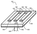
図6は、プリント基板の製造技術によって、本発明のアンテナを構成した実施例の概要構成を示す説明図である。 FIG. 6 is an explanatory diagram showing a schematic configuration of an embodiment in which the antenna of the present invention is configured by a printed circuit board manufacturing technique.
プリント基板601の片面の導体箔が地板104となっており、他方の面の導体箔をエッチングにより除去したものが、給電素子102および無給電素子103となっており、先端はバラクタ106で接続されている。なお、本図においては、理解を容易にするため、導体箔の厚さを強調して描いている。
The conductive foil on one side of the printed
給電素子102の後端は、スルーホール602を介して同軸ケーブル108の軸線に接続され、無給電素子103の後端は、スルーホール603を介して地板104に接続される。
The rear end of the
図7は、誘電体の両面に銅箔を形成することで、本発明のアンテナを構成した実施例の概要構成を示す説明図である。 FIG. 7 is an explanatory diagram showing a schematic configuration of an embodiment in which an antenna of the present invention is configured by forming copper foil on both surfaces of a dielectric.
本態様は、誘電体共振アンテナの構造に類似するものである。本図においても、銅箔の厚さは強調して表示する。 This aspect is similar to the structure of a dielectric resonant antenna. Also in this figure, the thickness of the copper foil is highlighted.
高さが低い直方体形状の誘電体701は、の表面に導体箔として銅箔を貼り付ける(エッチングによって形成することとしても良い。)ことによって、給電素子102および無給電素子103を構成している。先端はバラクタ106で接続されている。
The
誘電体701は、導体板(銅板等)である地板104の上に設置され、無給電素子103の後端は地板104に接続される。給電素子102の後端は、同軸ケーブル108の軸線に接続されている。
The dielectric 701 is installed on the
さて、これらの実施例において、地板104が無限の広さを有すると過程すると、鏡像による打消効果があるため、アンテナ101を介して垂直偏波の電波のみが送受信されることとなる。
In these embodiments, if the
地板104の広さが有限となると、入力インピーダンスも変化し、水平偏波成分の放射が現れる。そして、地板104が小さくなればなるほど、地板104の上下方向の水平偏波成分の放射は強くなる。
When the width of the
しかしながら、地板104の水平方向への水平偏波の放射はそれほど大きくならず、垂直偏波が主体のままとなる。
However, the radiation of horizontally polarized waves in the horizontal direction of the
したがって、アンテナ101によれば、地板104がある程度小さくなっても、地板104の水平方向に対する垂直偏波の電波の送受信が可能である。
Therefore, according to the
地板104は、製品の筐体そのものを利用することもでき、この場合、偏波を含むアンテナ101の可変特性は、筐体の大きさや形状に依存する。
As the
また、地板104の大きさが通信に用いる波長のオーダーとなる場合には、地板104からの放射を考慮する必要もある。
In addition, when the size of the
したがって、筐体を地板104として用いる場合には、製品の全体形状を考慮して設計を行う必要がある。
Therefore, when the casing is used as the
ただし、このような態様を採用した場合であっても、垂直偏波の送受信が可能である、という本発明の特徴は維持される。 However, even if such a mode is adopted, the feature of the present invention that vertical polarization can be transmitted and received is maintained.
(設計の一例)
以下では、アンテナ101の詳細な形状や寸法を設計するためのシミュレーション手法について説明する。
(Example of design)
Hereinafter, a simulation method for designing the detailed shape and dimensions of the
アンテナ特性のシミュレーションには、モーメント法によるシミュレーションソフトウェアNEC(商標)を利用する。 For simulation of antenna characteristics, simulation software NEC (trademark) based on the moment method is used.
一般に、地板に垂直な棒状のアンテナ素子を有するモノポール型アンテナの各素子を折り曲げてL字形にすると、動作利得の変化はさほど大きくはない。たとえば、アンテナ素子の間隔を0.05波長に、長さを0.25波長に、太さを0.01波長にし、給電素子と無給電素子との間のリアクタンス値をX1=-20Ω、X2=15Ωとした場合、モノポール型アンテナの動作利得は5.21dBiであり、L字形にしても動作利得の低下は0.5dB程度である。 In general, when each element of a monopole antenna having a rod-shaped antenna element perpendicular to the ground plane is bent into an L shape, the change in operating gain is not so great. For example, the distance between the antenna elements is 0.05 wavelength, the length is 0.25 wavelength, the thickness is 0.01 wavelength, and the reactance value between the feeding element and the parasitic element is X 1 = -20Ω, When X 2 = 15Ω, the operating gain of the monopole antenna is 5.21 dBi, and even if it is L-shaped, the decrease in operating gain is about 0.5 dB.
しかしながら、L字型にした場合には、入力インピーダンスZinが、(25.75 - j5.51)Ωから、(0.98 - j10.94)Ωへと大きく変化し、特に実部が小さくなるために、整合がとれなくなることがある。 However, when the L-shape, the input impedance Z in is - from (25.75 j5.51) Ω, (0.98 - j10.94) greatly changes to Omega, in order in particular the real part becomes small, Inconsistency may be lost.
そこで、設計の際には、整合回路を別途用意しなくとも良いような諸元を探すことが望ましい。 Therefore, in designing, it is desirable to search for specifications that do not require a separate matching circuit.
さて、本アンテナでは、リアクタンス値を調整することで指向性を制御するが、両者の関係は非線型であり、また、制御可能なアンテナ特性の取り得る状態も不明であることが多い。したがって、所望のアンテナ特性を実現するリアクタンス値を解析的に求めることは困難である。 In this antenna, the directivity is controlled by adjusting the reactance value. However, the relationship between the two is non-linear, and the state in which controllable antenna characteristics can be obtained is often unknown. Therefore, it is difficult to analytically obtain a reactance value that realizes a desired antenna characteristic.
このため、アンテナ特性を、リアクタンス値から評価関数値を求める評価関数f(・)で表し、評価関数f(・)の値が最大化するようなリアクタンス値を最急勾配法を用いることにより、所望のアンテナ特性を実現するリアクタンス値を求める。 For this reason, the antenna characteristic is expressed by an evaluation function f (·) for obtaining an evaluation function value from the reactance value, and the reactance value that maximizes the value of the evaluation function f (·) is used by using the steepest gradient method. A reactance value that achieves desired antenna characteristics is obtained.
給電素子102と2つの無給電素子103との間のリアクタンス値をそれぞれX1,X2とすると、m = 1,2について、最急勾配法の繰り返し回数n回目のリアクタンス値の推定値Xm[n]は、以下のような漸化式によって求めることができる。
Xm[n+1] = Xm[n] +μ〔f(Xm + ΔX) - f(Xm)〕/ΔX
Assuming that the reactance values between the feeding
X m [n + 1] = X m [n] + μ [f (X m + ΔX)-f (X m )] / ΔX
ここで、ΔXは摂動ステップ、μはステップサイズである。 Here, ΔX is a perturbation step, and μ is a step size.
本実施形態では、放射ビームを形成することとなるので、評価関数f(・)として利得を用いる。 In this embodiment, since a radiation beam is formed, a gain is used as the evaluation function f (•).
最急勾配法ではリアクタンス値Xmを微小変化させるごとに、アンテナ特性を計算しなおす必要がある。一方で、モーメント法による解析は計算量が大きいため、アンテナ特性の再計算をできるだけ簡易なものにしたい。 In the steepest gradient method every time to minutely change the reactance value X m, it is necessary to recalculate the antenna characteristics. On the other hand, the analysis by the moment method is computationally intensive, so we want to make the recalculation of antenna characteristics as simple as possible.
ところが、アンテナ構造はリアクタンス値に依存しない。アンテナ構造を定数パラメータ(構造パラメータ)として表現することとする。上記のように、アンテナ特性をリアクタンス値Xmのみを引き数とする関数f(・)として表現する。 However, the antenna structure does not depend on the reactance value. The antenna structure is expressed as a constant parameter (structure parameter). As described above, the antenna characteristics are expressed as a function f (·) having only the reactance value X m as an argument.
たとえば、等価ステアリングベクトルモデルを用いることにより、アンテナ101による遠方電界E(θ,φ)は、以下のように表現することができる。
For example, by using an equivalent steering vector model, the far electric field E (θ, φ) by the
ここで、M = 2であり、m = 0は給電素子102を、m = 1,2は無給電素子103を表す。
Here, M = 2, m = 0 represents the
また、um (v)(θ,φ)は、m番目のアンテナ素子(給電素子102もしくは無給電素子103)のポート電圧として単位電圧を与えたときの電界の方向依存性を表し、vmはm番目のアンテナ素子に対するポート電圧であり、Zm,nをポートmとポートnの間のインピーダンスとし、給電素子102に対して給電回路(RF信号通信機109に相当するもの。)が与える開放電圧vs、給電回路の内部インピーダンスZsとすると、以下のような計算が可能である。
Further, u m (v) (θ , φ) represents the electric field direction dependence of the time of giving the unit voltage as a port voltage of the m-th antenna element (feed
ここで、Zm,nはリアクタンスXmに依存しない構造パラメータであるから、um (v)(θ,φ)とともに、NECによる繰り返し計算を行う前に一度計算しておけば、あとは定数として扱うことができる。 Here, since Z m, n is a structural parameter that does not depend on reactance X m , if it is calculated once before iterative calculation by NEC together with u m (v) (θ, φ), the rest is a constant. Can be treated as
これらに基づけば、絶対利得Gaは、以下のように計算できる。ここで、rはアンテナからの距離、Zoは自由空間のインピーダンス、Zinは入力インピーダンスを意味する。 Based on these, the absolute gain Ga can be calculated as follows. Here, r is the distance from the antenna, Z o is the free space impedance, and Z in is the input impedance.
絶対利得Gaや入力インピーダンスZinはZsに依存しないので、上記の計算においては、Zs = 0として、計算を簡単にすることができる。 The absolute gain Ga and the input impedance Z in is not dependent on Z s, in the above calculation, as Z s = 0, calculation can be simplified.
上記のように、外部に整合回路を設置しなくても整合のとれる構造によりコストダウンを図ることとする。したがって、整合特性を含んだ動作利得Gwを評価関数とする。動作利得Gwは次式で計算できる。 As described above, the cost can be reduced by a structure that can achieve matching without installing a matching circuit outside. Therefore, the operation gain Gw including matching characteristics is used as an evaluation function. The operating gain Gw can be calculated by the following equation.
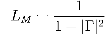
ここでLMは不整合損を意味し、反射係数をΓとすると、以下のように計算することができる。 Now means L M mismatching loss, the reflection coefficient and gamma, it can be calculated as follows.
反射係数Γと不整合損LMの計算では、Zsとして実際の値を用いる必要があり、同軸ケーブル108をアンテナ101に接続する場合には、Zs = 50Ωということになる。
In the calculation of the reflection coefficient Γ and the mismatch loss L M , it is necessary to use an actual value as Z s , and when the
(設計例1)
以下では、モノポール型アンテナに比べて、高さが約3分の1になるようなアンテナを設計してみる。
(Design example 1)
In the following, we will design an antenna that is about one-third the height of a monopole antenna.
たとえば、自由空間における電波波長をλとし、
給電素子102と無給電素子103との間隔d = 0.05λ;
給電素子102・無給電素子103と、地板104との距離(L字形の短辺の長さ)L = 0.08λ;
給電素子102・無給電素子103の、地板104に平行な長さ(L字形の長辺の長さ)L = 0.152λ;
給電素子102・無給電素子103の、線太さ(直径)W = 0.01λ
とすると、Zs = 50Ωとすることができ、整合がとれる。
For example, let λ be the radio wave wavelength in free space,
Distance between the
Distance between the
The length of the
Line thickness (diameter) W = 0.01λ of the
Then, Z s = 50Ω can be obtained, and matching can be obtained.
このとき、地板104に平行な水平面において、φ=90度の方向、すなわち、給電素子102・無給電素子103の配列方向(給電素子102・無給電素子103の長辺に垂直な方向)における動作利得が最大となるように、最急勾配法によりリアクタンスを求めると、
X1 = 5001.3Ω;
X2 = -4934.3Ω
となった。
At this time, in a horizontal plane parallel to the
X 1 = 5001.3Ω;
X 2 = -4934.3Ω
It became.
図8は、設計例1において、このリアクタンス値を採用し、φを変化させたときの動作利得パターンを示すグラフである。 FIG. 8 is a graph showing an operation gain pattern when the reactance value is adopted and φ is changed in Design Example 1.
本図において、横軸はφであり、太線は動作利得(整合のとれた4分の1波長モノポール型アンテナに対する相対値)を、細線は位相をそれぞれ表す。また、破線はリアクタンスをX1とX2とで交換した場合を表す。 In this figure, the horizontal axis represents φ, the thick line represents the operating gain (relative value with respect to the matched quarter-wave monopole antenna), and the thin line represents the phase. A broken line represents a case where the reactance is exchanged between X 1 and X 2 .
本図によれば、動作利得は、モノポール型アンテナに対して約4.3dB程度向上している。 According to this figure, the operating gain is improved by about 4.3 dB with respect to the monopole antenna.
しかしながら、上記のように、X1,X2の絶対値が大きい。バラクタ106の特性として、低周波数帯ではリアクタンスの可変幅が広いため、これらの値を実現することは容易である。しかしながら、高周波数帯では、これらの値を実現するための工夫をするか、あるいは、他の値を採用した場合の特性が所望の範囲に入っているかを確認する必要がある。
However, as described above, the absolute values of X 1 and X 2 are large. As the characteristics of the
たとえば、バラクタ106として、電気容量が9pFから0.7pFまで変化するものを採用すると、400MHz帯におけるリアクタンスの可変幅は約520Ωであり、1つでは、上記のX1,X2は実現できない。
For example, when a
バラクタを直列接続すれば、リアクタンス可変範囲を広げることができるが、制御電圧もその数に相当する分だけ高くしなければならない、という欠点がある。 If the varactors are connected in series, the reactance variable range can be expanded, but there is a disadvantage that the control voltage must be increased by an amount corresponding to the number.
バラクタ106をインダクタと並列接続すれば可変範囲を広げることができるが、並列共振状態を利用するため、素子の抵抗成分によりリアクタンス値がずれたり、損失が増加したりする欠点がある。
If the
そこで、リアクタンス値X1とX2の値を変化させた場合の、入力インピーダンスZin、電圧定在波比(Voltage Standing Wave Ratio) vswr、不整合損LM、動作利得(モノポールに対する相対値) Gaをシミュレーションにより求めた。 Therefore, input impedance Z in , voltage standing wave ratio (Voltage Standing Wave Ratio) vswr, mismatch loss L M , operating gain (relative to monopole) when reactance values X 1 and X 2 are changed. ) Ga was obtained by simulation.
図9は、設計例1において、リアクタンス値X1とX2の値を変化させた場合の、アンテナ特性の上記諸元を表す表である。以下、本図を参照して説明する。 FIG. 9 is a table showing the above-mentioned specifications of the antenna characteristics when the reactance values X 1 and X 2 are changed in Design Example 1. Hereinafter, a description will be given with reference to FIG.
本図に示すように、X1とX2の絶対値を小さくすると、動作利得Gaが低下するとともに、整合が劣化する。 As shown in this figure, when the absolute values of X 1 and X 2 are reduced, the operating gain Ga is lowered and the matching is deteriorated.
もっとも、X1 = 2000Ω、X2 = -2000Ω程度にしても、相対利得は約3dB程度向上しており、整合もvswr = 1.64程度で、用途によっては、これで十分な場合もある。 However, even if X 1 = 2000Ω and X 2 = −2000Ω, the relative gain is improved by about 3 dB and the matching is about vswr = 1.64, which may be sufficient depending on the application.
このように、バラクタ106を制御することによって指向性や整合の特性が変化するから、バラクタ106の調整によって、指向性を改善すると同時に、整合を改善することができる。
Thus, since the directivity and matching characteristics change by controlling the
(設計例2)
以下では、以下では、モノポール型アンテナに比べて、高さが約5分の1になるようなアンテナを設計してみる。
(Design example 2)
In the following, an antenna is designed so that its height is about one fifth that of a monopole antenna.
自由空間における電波波長をλに対して、
給電素子102と無給電素子103との間隔d = 0.04λ;
給電素子102・無給電素子103と、地板104との距離(L字形の短辺の長さ)L = 0.045λ;
給電素子102・無給電素子103の、地板104に平行な長さ(L字形の長辺の長さ)L = 0.195λ;
給電素子102・無給電素子103の、線太さ(直径)W = 0.012λ
とする。
For radio wave wavelength in free space,
Spacing d between the
Distance between the
The length of the
Line thickness (diameter) W of the
And
上記設計例と同様にリアクタンス値を求めると、
X1 = 1522.2Ω;
X2 = -1436.4Ω
となった。
When the reactance value is obtained in the same manner as the above design example,
X 1 = 1522.2Ω;
X 2 = -1436.4Ω
It became.
図10は、設計例2においてこのリアクタンス値を採用し、φを変化させたときの動作利得パターンを示すグラフである。 FIG. 10 is a graph showing an operation gain pattern when this reactance value is employed in design example 2 and φ is changed.
この結果を見ると、動作利得は、モノポールより約0.9dB大きくなることが分かる。 From this result, it can be seen that the operating gain is about 0.9 dB greater than the monopole.
図11は、設計例2において、リアクタンス値X1とX2の値を変化させた場合の、アンテナ特性を表す表である。 FIG. 11 is a table showing antenna characteristics when reactance values X 1 and X 2 are changed in design example 2.
本図によれば、リアクタンス値を変化させたとしても、vswr≦3となっており、この程度の整合が実現されていることがわかる。 According to this figure, it can be seen that even if the reactance value is changed, vswr ≦ 3, and this degree of matching is realized.
また、直流電圧の向きを変えれば、利得は低いものの、指向性ダイバーシティ効果が得られることがわかる。 It can also be seen that if the direction of the DC voltage is changed, the directional diversity effect can be obtained although the gain is low.
設計例1、設計例2において、リアクタンス値X1、X2を交換した場合の相関係数の自乗値は、それぞれ、0.162、0.748であり、位相パターンは給電素子102(給電ポート)に対して対称に切り換わっている。 In design example 1 and design example 2, when the reactance values X 1 and X 2 are exchanged, the square values of the correlation coefficients are 0.162 and 0.748, respectively, and the phase pattern is the feed element 102 (feed port). ) Is switched symmetrically.
このような特性は、モノポールから構成される電子走査導波器アレーアンテナとは異なる。むしろ、ループから構成されるRF-Feeder and DC-control Line Sharing Frequency Controllable Loopアンテナ([非特許文献3])に類似するものである。 Such characteristics are different from those of an electronic scanning waveguide array antenna composed of monopoles. Rather, it is similar to an RF-Feeder and DC-control Line Sharing Frequency Controllable Loop antenna ([Non-Patent Document 3]) composed of loops.
(電流分布)
以下では、上記の設計例1(モノポールの約3分の1の高さ)、設計例2(モノポールの約5分の1の高さ)において利得最大としたときの、アンテナ素子のL字形の短辺(地板104に垂直な部分)に流れる電流分布の振幅と位相とを、給電素子102と無給電素子103とで対比する。
(Current distribution)
Hereinafter, the antenna element L when the gain is maximized in the above-described design example 1 (about one third of the height of the monopole) and design example 2 (about one fifth of the height of the monopole) will be described. The amplitude and phase of the current distribution flowing in the short side of the character (portion perpendicular to the ground plane 104) are compared between the
図12は、アンテナ素子(給電素子102、無給電素子103)の地板104に垂直な部分における電流の振幅と位相の分布を示すグラフである。以下、本図を参照して説明する。
FIG. 12 is a graph showing the amplitude and phase distribution of current in a portion perpendicular to the
本図(a)は、設計例1(モノポールの約3分の1の高さ)に対するものであり、本図(b)は、設計例2(モノポールの約5分の1の高さ)に対するものである。 This figure (a) is a thing with respect to the design example 1 (about 1/3 height of a monopole), and this figure (b) is the design example 2 (about 1/5 height of a monopole). ).
電流の振幅を見ると、給電素子102に流れる電流は、いずれの場合においても、無給電素子103に流れる電流よりも大きいことがわかる。
From the current amplitude, it can be seen that the current flowing through the
また、本図(a)の場合には、2つの無給電素子103に流れる電流の大きさはほぼ等しく、位相差はほぼ180度である。
In the case of FIG. 5A, the magnitudes of the currents flowing through the two
給電部があるモノポール部に比べ、両側のモノポール部に大きな電流が流れていることが分かる。 It can be seen that a larger current flows through the monopole portions on both sides than the monopole portion with the power feeding portion.
これらの特性は小径電子走査導波器アレーアンテナ([非特許文献2])と同様であり、エンドファイア形の励振によりビームが形成されていることが分かる。 These characteristics are the same as those of the small-diameter electron scanning waveguide array antenna ([Non-Patent Document 2]), and it can be seen that the beam is formed by the endfire type excitation.
また、電流の振幅と位相から、いずれの場合も、2つの無給電素子103を含むループを回るような電流が流れていることがわかる。
Further, it can be seen from the amplitude and phase of the current that a current flowing around the loop including the two
上記設計例2を採用した場合、対応するモノポール型アンテナ以上の動作利得を持つためには、リアクタンス可変幅は2000Ω程度が必要となる(図11参照)。 When the design example 2 is adopted, the reactance variable width is required to be about 2000Ω in order to have an operation gain higher than that of the corresponding monopole antenna (see FIG. 11).
たとえば、容量可変範囲が9pFから0.7pFまで変化するバラクタを用いた場合、400MHz帯におけるリアクタンス可変幅は約520Ωとなるから、2000Ωのリアクタンス可変幅を実現するためには、バラクタを4個直列接続することとなる。 For example, when a varactor whose capacitance variable range changes from 9 pF to 0.7 pF is used, the reactance variable width in the 400 MHz band is about 520 Ω. Will be connected.
以下では、バラクタの直列数を2個(リアクタンス可変幅は約1000Ω)としたときに、得られる利得がどの程度となるかを調べる。 In the following, it is examined how much gain is obtained when the number of varactors in series is two (the reactance variable width is about 1000Ω).
このとき、整合を改善しやすくするために、給電素子102の途中にインダクタやコンデンサをリアクタとして接続するものとする。
At this time, in order to easily improve the matching, an inductor or a capacitor is connected as a reactor in the middle of the
図13は、給電素子102の途中にリアクタを挿入する様子を示す説明図である。以下、本図を参照して説明する。
FIG. 13 is an explanatory diagram illustrating a state in which a reactor is inserted in the middle of the
リアクタ801は、給電素子102の途中に挿入されるが、これは、無給電素子103と給電素子102との間にバラクタ106を接続するのと同様の技術によって実現することができる。
The reactor 801 is inserted in the middle of the
そして、リアクタ801のリアクタンス値X0の候補を選択する。それぞれに対して動作利得が大きくなるような給電素子102内におけるのリアクタ801の場所をモーメント法によるシミュレーションによって決定して、好適なリアクタンス値X0と場所を決定すれば良い。
Then, a candidate for the reactance value X 0 of the reactor 801 is selected. The location of the reactor 801 in the
リアクタ801を配置する場所は、給電素子102のL字形の角から先端へ向かう方向の距離L0によって表現する。ある設計例では、L0≒0.7L1となった。
The place where the reactor 801 is disposed is expressed by a distance L 0 in a direction from the L-shaped corner of the
さらに、動作利得が大きくなるようなL1の候補を複数モーメント法で求め、その候補の中から、X0の選択によって整合が改善するようなものを選択するのである。当該設計例では、L1 = 0.210λとしたときが最適である。 Further, candidates for L 1 that increase the operating gain are obtained by the multi-moment method, and those candidates whose matching is improved by selecting X 0 are selected from the candidates. In this design example, L 1 = 0.210λ is optimal.
次に、X1とX2のリアクタンス可変幅を1000Ωに固定して、整合がとれるX0の値と動作利得とを、最急勾配法で求める。この場合、最急勾配法における変数にX0が追加されることになる。さらに、可変幅を一定としたまま可変範囲を変更して、動作利得が最高となるリアクタンス可変範囲を求める。 Next, the reactance variable width of X 1 and X 2 is fixed to 1000Ω, and the value of X 0 and the operation gain that can be matched are obtained by the steepest gradient method. In this case, the X 0 is added to the variable in the steepest gradient method. Further, the variable range is changed while keeping the variable width constant, and the reactance variable range in which the operating gain is maximized is obtained.
当該設計例では、
X1 = 943.5Ω;
X2 = -56.5Ω;
X0 = 411.22Ω
が最適で、そのときの整合はvswr = 1.33であり、動作利得は、モノポール型アンテナに対する相対値でGw = 0.51dBmとなった。
In the design example,
X 1 = 943.5Ω;
X 2 = -56.5Ω;
X 0 = 411.22Ω
The matching at that time was vswr = 1.33, and the operating gain was Gw = 0.51 dBm relative to the monopole antenna.
図14は、この設計例における動作利得のパターンを示すグラフである。以下、本図を参照して説明する。 FIG. 14 is a graph showing an operation gain pattern in this design example. Hereinafter, a description will be given with reference to FIG.
本図に示すように、リアクタンス可変幅を設計例2の約3分の1にしたにもかかわらず、リアクタ801の装荷によって、同等の動作利得が得られている。 As shown in this figure, even though the reactance variable width is set to about one third of that in the design example 2, the equivalent operation gain is obtained by loading the reactor 801.
またこのときの、X1とX2の交換による相関係数自乗値は0.50であり、ダイバーシティ効果も有する。 At this time, the square of the correlation coefficient due to the exchange of X 1 and X 2 is 0.50, which also has a diversity effect.
なお、本実施例では、リアクタ801のリアクタンス値X0と、装荷位置L0を調整することとしたが、このほかの手法として、リアクタ801を追加せずに、給電素子102の長さLを変更することによって、調整することも可能である。この場合も、上記と同様の設計プロセスを採用することができる。
In this embodiment, the reactance value X 0 of the reactor 801 and the loading position L 0 are adjusted. However, as another method, the length L of the
以上説明したように、本発明によれば、垂直偏波の送受信が可能で、小型にするのに好適なアンテナを提供することができる。 As described above, according to the present invention, it is possible to provide an antenna that can transmit and receive vertically polarized waves and is suitable for miniaturization.
101 アンテナ
102 給電素子
103 無給電素子
104 地板
105 信号端子
106 バラクタ
108 同軸ケーブル
109 RF信号通信機
110 コンデンサ
111 電圧印加部
112 抵抗
113 抵抗
114 コンデンサ
115 抵抗
116 バラクタ
601 プリント基板
602 スルーホール
603 スルーホール
701 誘電体
801 リアクタ
DESCRIPTION OF
Claims (9)
前記地板に平行な棒形状を有し、等間隔に平行に配置され、前記地板からの距離が相等しい3つのアンテナ素子、
前記3つのアンテナ素子のうち中央のアンテナ素子である給電素子の先端と、当該給電素子以外の2つのアンテナ素子である無給電素子の先端のそれぞれと、を、接続する2つのバラクタ、
前記地板と、当該給電素子の後端と、の間の電位差の変化により信号を伝達する信号端子
を備え、前記2つのバラクタのリアクタンスを変化させることにより、前記地板に平行な面内において指向性を変化させる
ことを特徴とするアンテナ。 A conductive ground plane having a substantially planar shape and a finite size ,
Three antenna elements having a bar shape parallel to the ground plane, arranged in parallel at equal intervals, and equal in distance from the ground plane ,
Two varactors that connect the tip of a feeding element that is a central antenna element among the three antenna elements and each of the tips of parasitic elements that are two antenna elements other than the feeding element,
A signal terminal for transmitting a signal by a change in potential difference between the ground plane and a rear end of the feeding element; and by changing a reactance of the two varactors, directivity is achieved in a plane parallel to the ground plane. An antenna characterized by changing .
前記地板と、当該2つの無給電素子の後端のそれぞれと、の間に接続される2つの容量素子、
当該2つの無給電素子の後端の間に直流電圧を印加する電圧印加部
をさらに備え、
前記2つのバラクタは、逆方向に接続される
ことを特徴とするアンテナ。 The antenna according to claim 1,
Two capacitive elements connected between the ground plane and each of the rear ends of the two parasitic elements;
A voltage applying unit for applying a DC voltage between the rear ends of the two parasitic elements;
The antenna is characterized in that the two varactors are connected in opposite directions.
前記地板と、当該2つの無給電素子の後端のそれぞれとは、接続され、
前記2つのバラクタは、順方向に接続される
ことを特徴とするアンテナ。 The antenna according to claim 1,
The ground plate and each of the rear ends of the two parasitic elements are connected,
The antenna is characterized in that the two varactors are connected in a forward direction.
前記3つのアンテナ素子は、L字型の形状を有し、当該L字型の長辺は、前記地板と平行な棒形状を有し、当該L字型の短辺は、前記地板に垂直な棒形状を有する
ことを特徴とするアンテナ。 The antenna according to any one of claims 1 to 3,
The three antenna elements have an L-shape, the long side of the L-shape has a bar shape parallel to the ground plane, and the short side of the L-shape is perpendicular to the ground plane. An antenna characterized by having a bar shape.
前記3つのアンテナ素子と、前記地板と、の間を充填する誘電体
をさらに備えることを特徴とするアンテナ。 The antenna according to claim 4, wherein
The antenna further comprising: a dielectric material filling the space between the three antenna elements and the ground plane.
前記地板は、プリント基板の片面に配置される導電性箔であり、前記3つのアンテナ素子は、当該プリント基板の反対面に配置される導電性箔であり、前記3つのアンテナ素子のそれぞれの後端は、当該プリント基板のスルーホールを通過して接続される
ことを特徴とするアンテナ。 The antenna according to any one of claims 1 to 3,
The ground plane is a conductive foil disposed on one side of the printed circuit board, and the three antenna elements are conductive foils disposed on the opposite surface of the printed circuit board. The antenna is characterized in that the end is connected through the through hole of the printed circuit board.
当該給電素子にインダクタもしくはコンデンサを接続して、所望のリアクタンス可変幅における動作利得を最大化した
ことを特徴とするアンテナ。 The antenna according to any one of claims 1 to 6,
An antenna characterized in that an operating gain in a desired reactance variable width is maximized by connecting an inductor or a capacitor to the feeding element.
前記3つのアンテナ素子同士の間隔は、通信に用いる波長の0.04倍であり、
前記3つのアンテナ素子の長さは、当該波長の0.195倍であり、
前記3つのアンテナ素子と前記地板との間隔は、当該波長の0.045倍であり、
前記3つのアンテナ素子の直径は、当該波長の0.012倍である
ことを特徴とするアンテナ。 The antenna according to any one of claims 1 to 7,
The interval between the three antenna elements is 0.04 times the wavelength used for communication,
The length of the three antenna elements is 0.195 times the wavelength,
The distance between the three antenna elements and the ground plane is 0.045 times the wavelength,
The diameter of the three antenna elements is 0.012 times the wavelength.
当該給電素子の長さを、当該無給電素子の長さと異なるものとして、所望のリアクタンス可変幅における動作利得を最大化した
ことを特徴とするアンテナ。 The antenna according to any one of claims 1 to 6,
An antenna characterized in that the length of the feed element is different from the length of the parasitic element and the operation gain in a desired reactance variable width is maximized.
Priority Applications (1)
| Application Number | Priority Date | Filing Date | Title |
|---|---|---|---|
| JP2006218503A JP4714876B2 (en) | 2006-08-10 | 2006-08-10 | antenna |
Applications Claiming Priority (1)
| Application Number | Priority Date | Filing Date | Title |
|---|---|---|---|
| JP2006218503A JP4714876B2 (en) | 2006-08-10 | 2006-08-10 | antenna |
Publications (2)
| Publication Number | Publication Date |
|---|---|
| JP2008042852A JP2008042852A (en) | 2008-02-21 |
| JP4714876B2 true JP4714876B2 (en) | 2011-06-29 |
Family
ID=39177327
Family Applications (1)
| Application Number | Title | Priority Date | Filing Date |
|---|---|---|---|
| JP2006218503A Expired - Fee Related JP4714876B2 (en) | 2006-08-10 | 2006-08-10 | antenna |
Country Status (1)
| Country | Link |
|---|---|
| JP (1) | JP4714876B2 (en) |
Cited By (1)
| Publication number | Priority date | Publication date | Assignee | Title |
|---|---|---|---|---|
| CN109983622A (en) * | 2016-12-16 | 2019-07-05 | 株式会社友华 | Antenna assembly |
Families Citing this family (6)
| Publication number | Priority date | Publication date | Assignee | Title |
|---|---|---|---|---|
| CN101542839B (en) * | 2008-07-18 | 2013-08-14 | 香港应用科技研究院有限公司 | Direction-finding antenna system and using method thereof |
| JP2010041071A (en) * | 2008-07-31 | 2010-02-18 | Toshiba Corp | Antenna device |
| KR101874892B1 (en) | 2012-01-13 | 2018-07-05 | 삼성전자 주식회사 | Small antenna appartus and method for controling a resonance frequency of small antenna |
| WO2013140758A1 (en) * | 2012-03-21 | 2013-09-26 | 日本電気株式会社 | Antenna device |
| JP6218573B2 (en) * | 2013-11-27 | 2017-10-25 | 三菱電機株式会社 | Antenna device |
| JP7311390B2 (en) * | 2019-10-25 | 2023-07-19 | 矢崎総業株式会社 | antenna device |
Family Cites Families (7)
| Publication number | Priority date | Publication date | Assignee | Title |
|---|---|---|---|---|
| JPS56160015U (en) * | 1980-04-30 | 1981-11-28 | ||
| JPH11274843A (en) * | 1998-03-23 | 1999-10-08 | Tdk Corp | Antenna system |
| FR2828584A1 (en) * | 2001-08-10 | 2003-02-14 | Thomson Licensing Sa | Domestic/gymnasium/TV studio radiation diversity wireless transmission having central feed symmetrical slot antennas electromagnetically coupling and coplanar end electronic component switch each line end short/open circuit. |
| JP4195403B2 (en) * | 2004-03-01 | 2008-12-10 | 株式会社国際電気通信基礎技術研究所 | Antenna structure and television receiver |
| JP3987058B2 (en) * | 2004-06-17 | 2007-10-03 | 株式会社東芝 | Antenna device |
| JP2006005756A (en) * | 2004-06-18 | 2006-01-05 | Toshiba Corp | Antenna device |
| JP2006180225A (en) * | 2004-12-22 | 2006-07-06 | Advanced Telecommunication Research Institute International | Antenna device |
-
2006
- 2006-08-10 JP JP2006218503A patent/JP4714876B2/en not_active Expired - Fee Related
Cited By (1)
| Publication number | Priority date | Publication date | Assignee | Title |
|---|---|---|---|---|
| CN109983622A (en) * | 2016-12-16 | 2019-07-05 | 株式会社友华 | Antenna assembly |
Also Published As
| Publication number | Publication date |
|---|---|
| JP2008042852A (en) | 2008-02-21 |
Similar Documents
| Publication | Publication Date | Title |
|---|---|---|
| JP4481716B2 (en) | Communication device | |
| JP4231867B2 (en) | Wireless device and electronic device | |
| JP3735635B2 (en) | ANTENNA DEVICE AND RADIO COMMUNICATION DEVICE USING THE SAME | |
| JP4089680B2 (en) | Antenna device | |
| TWI411160B (en) | Antenna and communication device having same | |
| CN102484320B (en) | cross dipole antenna | |
| CN102800967B (en) | Antenna for a portable computer | |
| KR102057880B1 (en) | Compound loop antenna | |
| Rezaeieh et al. | Miniaturization of planar Yagi antennas using mu-negative metamaterial-loaded reflector | |
| US8487821B2 (en) | Methods and apparatus for a low reflectivity compensated antenna | |
| JP2007110723A (en) | Broadband antenna and method for manufacturing the same | |
| KR20060042232A (en) | Reverse f antenna | |
| US8427378B2 (en) | Electronic device having solar cell antenna element and related methods | |
| WO2019005252A1 (en) | Antenna loaded with electromechanical resonators | |
| JP6456506B2 (en) | Antenna device | |
| US6590543B1 (en) | Double monopole meanderline loaded antenna | |
| JP4714876B2 (en) | antenna | |
| JP4863378B2 (en) | Antenna device | |
| US6791502B2 (en) | Stagger tuned meanderline loaded antenna | |
| Di Nallo et al. | Wideband antenna using non-Foster loading elements | |
| Bit-Babik et al. | Small wideband antenna with non-foster loading elements | |
| JP4329579B2 (en) | Antenna device | |
| JP4734655B2 (en) | Antenna device | |
| WO2021119077A1 (en) | Anisotropic constitutive parameters for launching a zenneck surface wave | |
| CN220963757U (en) | Antenna and electronic equipment |
Legal Events
| Date | Code | Title | Description |
|---|---|---|---|
| A621 | Written request for application examination |
Free format text: JAPANESE INTERMEDIATE CODE: A621 Effective date: 20090526 |
|
| A977 | Report on retrieval |
Free format text: JAPANESE INTERMEDIATE CODE: A971007 Effective date: 20100728 |
|
| A131 | Notification of reasons for refusal |
Free format text: JAPANESE INTERMEDIATE CODE: A131 Effective date: 20100803 |
|
| A521 | Request for written amendment filed |
Free format text: JAPANESE INTERMEDIATE CODE: A523 Effective date: 20100929 |
|
| A01 | Written decision to grant a patent or to grant a registration (utility model) |
Free format text: JAPANESE INTERMEDIATE CODE: A01 Effective date: 20110301 |
|
| A61 | First payment of annual fees (during grant procedure) |
Free format text: JAPANESE INTERMEDIATE CODE: A61 Effective date: 20110303 |
|
| R150 | Certificate of patent or registration of utility model |
Free format text: JAPANESE INTERMEDIATE CODE: R150 |
|
| FPAY | Renewal fee payment (event date is renewal date of database) |
Free format text: PAYMENT UNTIL: 20140408 Year of fee payment: 3 |
|
| R250 | Receipt of annual fees |
Free format text: JAPANESE INTERMEDIATE CODE: R250 |
|
| R250 | Receipt of annual fees |
Free format text: JAPANESE INTERMEDIATE CODE: R250 |
|
| S533 | Written request for registration of change of name |
Free format text: JAPANESE INTERMEDIATE CODE: R313533 |
|
| R350 | Written notification of registration of transfer |
Free format text: JAPANESE INTERMEDIATE CODE: R350 |
|
| R250 | Receipt of annual fees |
Free format text: JAPANESE INTERMEDIATE CODE: R250 |
|
| R250 | Receipt of annual fees |
Free format text: JAPANESE INTERMEDIATE CODE: R250 |
|
| LAPS | Cancellation because of no payment of annual fees |