JP4744975B2 - チルト回路 - Google Patents
チルト回路 Download PDFInfo
- Publication number
- JP4744975B2 JP4744975B2 JP2005230816A JP2005230816A JP4744975B2 JP 4744975 B2 JP4744975 B2 JP 4744975B2 JP 2005230816 A JP2005230816 A JP 2005230816A JP 2005230816 A JP2005230816 A JP 2005230816A JP 4744975 B2 JP4744975 B2 JP 4744975B2
- Authority
- JP
- Japan
- Prior art keywords
- frequency
- circuit
- blocking capacitor
- high frequency
- pin
- Prior art date
- Legal status (The legal status is an assumption and is not a legal conclusion. Google has not performed a legal analysis and makes no representation as to the accuracy of the status listed.)
- Expired - Fee Related
Links
Images

Landscapes
- Cable Transmission Systems, Equalization Of Radio And Reduction Of Echo (AREA)
Description
54 LC並列共振回路(リアクタンス並列共振手段)
Claims (1)
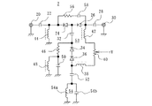
- 入力端子に第1の直流阻止コンデンサを介して一端が接続され、出力端子に第2の直流阻止コンデンサを介して他端が接続された第1及び第2のPINダイオードの直列回路を有し、第1及び第2のPINダイオードの相互接続点に第3の直流阻止コンデンサを介して第3のPINダイオードの一端が接続された減衰手段と、
第3のPINダイオードの他端に第4の直流阻止コンデンサを介して一端が接続され、他端が共通電位に接続され、前記入力端子に供給される高周波信号の高域側で共振する並列共振手段と、
第1の直流阻止コンデンサ並びに第1及び第2のPINダイオードの直列回路の接続点と前記共通電位との間に、接続された第1の直流通路と、
第3の直流阻止コンデンサ及び第3のPINダイオードの接続点と前記共通電位との間に接続された第2の直流通路と、
第2の直流阻止コンデンサと第1及び第2のPINダイオードの直列回路との接続点と、第3のPINダイオードダイオードと第4の直流阻止コンデンサとの接続点とに、両端が接続され、摺動子に直流電圧が供給されている可変抵抗器と、
第1及び第2のPINダイオードの直列回路に並列に接続された、抵抗器と第5の直流阻止コンデンサとの直列回路とを、
具備するチルト回路。
Priority Applications (1)
| Application Number | Priority Date | Filing Date | Title |
|---|---|---|---|
| JP2005230816A JP4744975B2 (ja) | 2005-08-09 | 2005-08-09 | チルト回路 |
Applications Claiming Priority (1)
| Application Number | Priority Date | Filing Date | Title |
|---|---|---|---|
| JP2005230816A JP4744975B2 (ja) | 2005-08-09 | 2005-08-09 | チルト回路 |
Publications (2)
| Publication Number | Publication Date |
|---|---|
| JP2007049355A JP2007049355A (ja) | 2007-02-22 |
| JP4744975B2 true JP4744975B2 (ja) | 2011-08-10 |
Family
ID=37851831
Family Applications (1)
| Application Number | Title | Priority Date | Filing Date |
|---|---|---|---|
| JP2005230816A Expired - Fee Related JP4744975B2 (ja) | 2005-08-09 | 2005-08-09 | チルト回路 |
Country Status (1)
| Country | Link |
|---|---|
| JP (1) | JP4744975B2 (ja) |
Family Cites Families (5)
| Publication number | Priority date | Publication date | Assignee | Title |
|---|---|---|---|---|
| JPS6339207A (ja) * | 1986-08-04 | 1988-02-19 | Nec Corp | 周波数振幅特性の等化器 |
| JPH0447805A (ja) * | 1990-06-15 | 1992-02-18 | Nec Corp | 振幅補償回路 |
| JP2829473B2 (ja) * | 1993-01-12 | 1998-11-25 | 日本アンテナ株式会社 | 高周波可変スロープチルト回路 |
| JPH06216688A (ja) * | 1993-01-13 | 1994-08-05 | Mitsubishi Electric Corp | 定インピーダンス電圧制御可変減衰器 |
| JP4017878B2 (ja) * | 2002-02-01 | 2007-12-05 | Dxアンテナ株式会社 | イコライザ |
-
2005
- 2005-08-09 JP JP2005230816A patent/JP4744975B2/ja not_active Expired - Fee Related
Also Published As
| Publication number | Publication date |
|---|---|
| JP2007049355A (ja) | 2007-02-22 |
Similar Documents
| Publication | Publication Date | Title |
|---|---|---|
| US8836447B2 (en) | Tuner and front-end circuit thereof | |
| JP2009130831A (ja) | チューナブルフィルタ | |
| US7639071B2 (en) | Active LC band pass filter | |
| WO2018012275A1 (ja) | マルチプレクサ、高周波フロントエンド回路、および、通信端末 | |
| JP5375521B2 (ja) | 高周波増幅器および無線通信装置 | |
| US7439811B2 (en) | Broadband low noise amplifier and RF signal amplification method of the same | |
| US20070188260A1 (en) | Receiver input circuit | |
| US7023294B2 (en) | System and a method for reducing tilt effects in a radio frequency attenuator | |
| CN101867349A (zh) | 射频功率放大器 | |
| JP2007104425A (ja) | 受信機入力回路 | |
| JP3734642B2 (ja) | 入力トラップ回路及びイメージトラップ回路 | |
| JP2007049355A (ja) | チルト回路 | |
| US6647253B2 (en) | High gain intermediate frequency input circuit with satisfactory trap characteristics | |
| JP2003229791A (ja) | イコライザ | |
| JP2008300956A (ja) | 受信機入力回路 | |
| JP2008294844A (ja) | テレビジョンチューナの複同調回路 | |
| JP2005217753A (ja) | 増幅器 | |
| JP4545811B2 (ja) | テレビジョンチューナ | |
| JPWO2006098059A1 (ja) | アンテナダンピング回路およびこれを用いた高周波受信機 | |
| JP5651266B1 (ja) | 光受信器のagc回路とagc回路を備えた光受信器 | |
| JPH09130285A (ja) | テレビジョンチューナの入力回路 | |
| JP4506719B2 (ja) | 高周波用可変減衰回路 | |
| JP2008228173A (ja) | 受信機入力回路 | |
| JP3103017U (ja) | テレビジョンチューナ | |
| JP2011049655A (ja) | テレビジョン信号受信チューナ |
Legal Events
| Date | Code | Title | Description |
|---|---|---|---|
| A621 | Written request for application examination |
Free format text: JAPANESE INTERMEDIATE CODE: A621 Effective date: 20080804 |
|
| A977 | Report on retrieval |
Free format text: JAPANESE INTERMEDIATE CODE: A971007 Effective date: 20101117 |
|
| A131 | Notification of reasons for refusal |
Free format text: JAPANESE INTERMEDIATE CODE: A131 Effective date: 20101124 |
|
| A521 | Written amendment |
Free format text: JAPANESE INTERMEDIATE CODE: A523 Effective date: 20110124 |
|
| TRDD | Decision of grant or rejection written | ||
| A01 | Written decision to grant a patent or to grant a registration (utility model) |
Free format text: JAPANESE INTERMEDIATE CODE: A01 Effective date: 20110510 |
|
| A01 | Written decision to grant a patent or to grant a registration (utility model) |
Free format text: JAPANESE INTERMEDIATE CODE: A01 |
|
| A61 | First payment of annual fees (during grant procedure) |
Free format text: JAPANESE INTERMEDIATE CODE: A61 Effective date: 20110511 |
|
| FPAY | Renewal fee payment (event date is renewal date of database) |
Free format text: PAYMENT UNTIL: 20140520 Year of fee payment: 3 |
|
| R150 | Certificate of patent or registration of utility model |
Free format text: JAPANESE INTERMEDIATE CODE: R150 |
|
| LAPS | Cancellation because of no payment of annual fees |