JP4754201B2 - 半導体装置 - Google Patents
半導体装置 Download PDFInfo
- Publication number
- JP4754201B2 JP4754201B2 JP2004298611A JP2004298611A JP4754201B2 JP 4754201 B2 JP4754201 B2 JP 4754201B2 JP 2004298611 A JP2004298611 A JP 2004298611A JP 2004298611 A JP2004298611 A JP 2004298611A JP 4754201 B2 JP4754201 B2 JP 4754201B2
- Authority
- JP
- Japan
- Prior art keywords
- pad
- pads
- group
- ground
- power supply
- Prior art date
- Legal status (The legal status is an assumption and is not a legal conclusion. Google has not performed a legal analysis and makes no representation as to the accuracy of the status listed.)
- Expired - Fee Related
Links
Images


Classifications
-
- H—ELECTRICITY
- H10—SEMICONDUCTOR DEVICES; ELECTRIC SOLID-STATE DEVICES NOT OTHERWISE PROVIDED FOR
- H10W—GENERIC PACKAGES, INTERCONNECTIONS, CONNECTORS OR OTHER CONSTRUCTIONAL DETAILS OF DEVICES COVERED BY CLASS H10
- H10W72/00—Interconnections or connectors in packages
-
- H—ELECTRICITY
- H10—SEMICONDUCTOR DEVICES; ELECTRIC SOLID-STATE DEVICES NOT OTHERWISE PROVIDED FOR
- H10W—GENERIC PACKAGES, INTERCONNECTIONS, CONNECTORS OR OTHER CONSTRUCTIONAL DETAILS OF DEVICES COVERED BY CLASS H10
- H10W70/00—Package substrates; Interposers; Redistribution layers [RDL]
- H10W70/60—Insulating or insulated package substrates; Interposers; Redistribution layers
- H10W70/62—Insulating or insulated package substrates; Interposers; Redistribution layers characterised by their interconnections
- H10W70/65—Shapes or dispositions of interconnections
-
- H—ELECTRICITY
- H10—SEMICONDUCTOR DEVICES; ELECTRIC SOLID-STATE DEVICES NOT OTHERWISE PROVIDED FOR
- H10W—GENERIC PACKAGES, INTERCONNECTIONS, CONNECTORS OR OTHER CONSTRUCTIONAL DETAILS OF DEVICES COVERED BY CLASS H10
- H10W70/00—Package substrates; Interposers; Redistribution layers [RDL]
- H10W70/60—Insulating or insulated package substrates; Interposers; Redistribution layers
- H10W70/62—Insulating or insulated package substrates; Interposers; Redistribution layers characterised by their interconnections
- H10W70/65—Shapes or dispositions of interconnections
- H10W70/654—Top-view layouts
- H10W70/655—Fan-out layouts
-
- H—ELECTRICITY
- H10—SEMICONDUCTOR DEVICES; ELECTRIC SOLID-STATE DEVICES NOT OTHERWISE PROVIDED FOR
- H10W—GENERIC PACKAGES, INTERCONNECTIONS, CONNECTORS OR OTHER CONSTRUCTIONAL DETAILS OF DEVICES COVERED BY CLASS H10
- H10W90/00—Package configurations
- H10W90/701—Package configurations characterised by the relative positions of pads or connectors relative to package parts
- H10W90/751—Package configurations characterised by the relative positions of pads or connectors relative to package parts of bond wires
- H10W90/754—Package configurations characterised by the relative positions of pads or connectors relative to package parts of bond wires between a chip and a stacked insulating package substrate, interposer or RDL
Landscapes
- Lead Frames For Integrated Circuits (AREA)
- Semiconductor Integrated Circuits (AREA)
Description
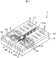
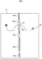
直線状に並べられた複数のパッドを含む半導体チップであって、当該半導体チップは前記基板の前記開口部から前記複数のパッドが露出するように前記基板に実装され、前記複数のパッドは、第1のパッド群と当該第1のパッド群との間に前記複数のパッドのうちの残りのいかなるパッドも挟み込むことなく前記第1のパッド群に隣接して配置される第2のパッド群とを含み、当該第1及び第2の
パッド群の各々は、電源パッドとグランドパッドと2つの信号パッドとを含む、前記半導体チップと、
前記第1のパッド群を前記第1の接続端子群のうちの対応する複数の端子群に接続する第1の配線群と、
前記第2のパッド群を前記第2の接続端子群のうちの対応する複数の端子群に接続する第2の配線群と、を備え、
前記第1の領域及び前記第2の領域は、前記第1の配線群が第1の方向に延伸し、前記第2の配線群が前記第1の方向と反対の第2の方向に延伸するように配置され、
前記第1のパッド群に含まれる全てのパッドから延伸する全ての配線は前記第1の方向に延伸し、
前記第2のパッド群に含まれる全てのパッドから延伸する全ての配線は前記第2の方向に延伸することを特徴とする半導体装置を提供する。
Claims (6)
- 開口部を含む基板であって、前記開口部は、当該開口部を挟んで対向する第1及び第2の領域によって規定され、前記基板は、前記第1の領域に配置された第1の接続端子群と前記第2の領域に配置された第2の接続端子群とをさらに備える、前記基板と、
直線状に並べられた複数のパッドを含む半導体チップであって、当該半導体チップは前記基板の前記開口部から前記複数のパッドが露出するように前記基板に実装され、前記複数のパッドは、第1のパッド群と当該第1のパッド群との間に前記複数のパッドのうちの残りのいかなるパッドも挟み込むことなく前記第1のパッド群に隣接して配置される第2のパッド群とを含み、当該第1及び第2の
パッド群の各々は、電源パッドとグランドパッドと2つの信号パッドとを含む、前記半導体チップと、
前記第1のパッド群を前記第1の接続端子群のうちの対応する複数の端子群に接続する第1の配線群と、
前記第2のパッド群を前記第2の接続端子群のうちの対応する複数の端子群に接続する第2の配線群と、を備え、
前記第1の領域及び前記第2の領域は、前記第1の配線群が第1の方向に延伸し、前記第2の配線群が前記第1の方向と反対の第2の方向に延伸するように配置され、
前記第1のパッド群に含まれる全てのパッドから延伸する全ての配線は前記第1の方向に延伸し、
前記第2のパッド群に含まれる全てのパッドから延伸する全ての配線は前記第2の方向に延伸することを特徴とする半導体装置。 - 前記複数のパッドは、第3のパッド群と、前記第2のパッド群と前記第3のパッド群とに挟まれた第4のパッド群とをさらに含み、前記第3及び第4のパッド群の各々は、電源パッドとグランドパッドと2つの信号パッドとを含み、前記第3のパッド群を前記第2の接続端子群のうちの対応する複数の端子群に接続する第3の配線群と、前記第4のパッド群を前記第1の接続端子群のうちの対応する複数の端子群に接続する第4の配線群とをさらに含むことを特徴とする請求項1に記載の半導体装置。
- 前記第3のパッド群に含まれる全てのパッドから延伸する全ての配線は前記第2の方向に延伸し、
前記第4のパッド群に含まれる全てのパッドから延伸する全ての配線は前記第1の方向に延伸することを特徴とする請求項2に記載の半導体装置。 - 前記第1及び第2のパッド群の夫々において、前記電源パッドと前記グランドパッドとが、前記2つの信号パッドの間にはさまれていることを特徴とする請求項1に記載の半導体装置。
- 前記半導体チップは、複数の入出力回路を含み、前記第1及び第2のパッド群の夫々の前記2つの信号パッドは、前記複数の入出力回路のうちの2つの入出力回路にそれぞれ対応して電気的に接続され、前記第1及び第2のパッド群の夫々の前記電源パッドと前記グランドパッドの各々は、前記2つの入出力回路に共通に電気的に接続されることを特徴とする請求項1に記載の半導体装置。
- 前記半導体チップ上の全ての前記電源パッドと前記グランドパッドの総数を、前記半導体チップ上に配置可能な前記複数のパッドの総数で除した値が、0.4よりも大きいことを特徴とする請求項1に記載の半導体装置。
Priority Applications (2)
| Application Number | Priority Date | Filing Date | Title |
|---|---|---|---|
| JP2004298611A JP4754201B2 (ja) | 2004-10-13 | 2004-10-13 | 半導体装置 |
| US11/247,215 US8362614B2 (en) | 2004-10-13 | 2005-10-12 | Fine pitch grid array type semiconductor device |
Applications Claiming Priority (1)
| Application Number | Priority Date | Filing Date | Title |
|---|---|---|---|
| JP2004298611A JP4754201B2 (ja) | 2004-10-13 | 2004-10-13 | 半導体装置 |
Publications (2)
| Publication Number | Publication Date |
|---|---|
| JP2006114595A JP2006114595A (ja) | 2006-04-27 |
| JP4754201B2 true JP4754201B2 (ja) | 2011-08-24 |
Family
ID=36179878
Family Applications (1)
| Application Number | Title | Priority Date | Filing Date |
|---|---|---|---|
| JP2004298611A Expired - Fee Related JP4754201B2 (ja) | 2004-10-13 | 2004-10-13 | 半導体装置 |
Country Status (2)
| Country | Link |
|---|---|
| US (1) | US8362614B2 (ja) |
| JP (1) | JP4754201B2 (ja) |
Families Citing this family (7)
| Publication number | Priority date | Publication date | Assignee | Title |
|---|---|---|---|---|
| JP2008060215A (ja) * | 2006-08-30 | 2008-03-13 | Elpida Memory Inc | 半導体装置 |
| KR101211683B1 (ko) * | 2008-12-31 | 2012-12-12 | 에스케이하이닉스 주식회사 | 반도체 집적회로 |
| JP2010192680A (ja) * | 2009-02-18 | 2010-09-02 | Elpida Memory Inc | 半導体装置 |
| US9123713B2 (en) * | 2010-11-24 | 2015-09-01 | Tessera, Inc. | Lead structures with vertical offsets |
| JP2012209296A (ja) * | 2011-03-29 | 2012-10-25 | Elpida Memory Inc | 半導体集積回路装置 |
| KR20150100388A (ko) | 2014-02-25 | 2015-09-02 | 삼성전자주식회사 | 메모리 모듈의 모듈 탭 영역에서의 선택적 리세스드 레퍼런스 플레인 구조 및 그에 따른 선택적 리세스드 레퍼런스 플레인 형성방법 |
| JP6272173B2 (ja) * | 2014-07-31 | 2018-01-31 | 京セラ株式会社 | 配線基板 |
Family Cites Families (11)
| Publication number | Priority date | Publication date | Assignee | Title |
|---|---|---|---|---|
| JP3299342B2 (ja) * | 1993-06-11 | 2002-07-08 | 株式会社日立製作所 | 半導体メモリモジュール |
| JPH0738011A (ja) * | 1993-06-29 | 1995-02-07 | Hitachi Ltd | 半導体集積回路装置 |
| US5604710A (en) * | 1994-05-20 | 1997-02-18 | Mitsubishi Denki Kabushiki Kaisha | Arrangement of power supply and data input/output pads in semiconductor memory device |
| US5714801A (en) * | 1995-03-31 | 1998-02-03 | Kabushiki Kaisha Toshiba | Semiconductor package |
| JPH10284678A (ja) * | 1997-04-03 | 1998-10-23 | Hitachi Ltd | 半導体装置およびその製造方法 |
| US6890796B1 (en) * | 1997-07-16 | 2005-05-10 | Oki Electric Industry Co., Ltd. | Method of manufacturing a semiconductor package having semiconductor decice mounted thereon and elongate opening through which electodes and patterns are connected |
| JP3480291B2 (ja) * | 1998-01-08 | 2003-12-15 | 日立電線株式会社 | 半導体装置及び電子装置 |
| JP2001185576A (ja) | 1999-12-27 | 2001-07-06 | Hitachi Ltd | 半導体装置 |
| KR100408391B1 (ko) * | 2000-06-09 | 2003-12-06 | 삼성전자주식회사 | 전원 배선을 개선한 볼그리드 어레이 패키지 반도체 장치 |
| JP2002217377A (ja) * | 2001-01-18 | 2002-08-02 | Hitachi Ltd | 半導体集積回路装置およびその製造方法 |
| US7323772B2 (en) * | 2002-08-28 | 2008-01-29 | Micron Technology, Inc. | Ball grid array structures and tape-based method of manufacturing same |
-
2004
- 2004-10-13 JP JP2004298611A patent/JP4754201B2/ja not_active Expired - Fee Related
-
2005
- 2005-10-12 US US11/247,215 patent/US8362614B2/en not_active Expired - Fee Related
Also Published As
| Publication number | Publication date |
|---|---|
| US20060081972A1 (en) | 2006-04-20 |
| US8362614B2 (en) | 2013-01-29 |
| JP2006114595A (ja) | 2006-04-27 |
Similar Documents
| Publication | Publication Date | Title |
|---|---|---|
| US20040145042A1 (en) | Semiconductor device | |
| US7663903B2 (en) | Semiconductor memory device having improved voltage transmission path and driving method thereof | |
| JP2007066922A (ja) | 半導体集積回路装置 | |
| TW201715692A (zh) | 半導體晶片模組及包含其之半導體封裝 | |
| US8633596B2 (en) | Semiconductor package with bonding wires of reduced loop inductance | |
| US20140097547A1 (en) | Semiconductor device | |
| US9478525B2 (en) | Semiconductor device | |
| US7960823B2 (en) | Semiconductor device with different sized ESD protection elements | |
| US6818983B2 (en) | Semiconductor memory chip and semiconductor memory device using the same | |
| JP4068616B2 (ja) | 半導体装置 | |
| US10679956B2 (en) | Semiconductor memory chip, semiconductor memory package, and electronic system using the same | |
| JP4754201B2 (ja) | 半導体装置 | |
| US20160056130A1 (en) | Semiconductor integrated circuit including power tsvs | |
| US20050104184A1 (en) | Semiconductor chip package and method | |
| JP2006165077A (ja) | 積層型半導体パッケージ | |
| US7847377B2 (en) | Semiconductor device including semiconductor chip with two pad rows | |
| CN101197365B (zh) | 半导体存储装置 | |
| JP5543094B2 (ja) | 低ノイズ半導体パッケージ | |
| KR100359591B1 (ko) | 반도체 장치 | |
| JP3846777B2 (ja) | ボールグリッドアレイパッケージ | |
| US20240387462A1 (en) | Semiconductor device and semiconductor package including the same | |
| KR100570580B1 (ko) | 반도체 장치 | |
| US20060220263A1 (en) | Semiconductor device to be applied to various types of semiconductor package | |
| US8039965B2 (en) | Semiconductor device with reduced layout area having shared metal line between pads | |
| KR20020014643A (ko) | 기판의 배선을 통하여 반도체 칩 내부전원을 일정하게공급하는 볼 그리드 어레이 패키지 |
Legal Events
| Date | Code | Title | Description |
|---|---|---|---|
| A711 | Notification of change in applicant |
Free format text: JAPANESE INTERMEDIATE CODE: A711 Effective date: 20070220 |
|
| RD01 | Notification of change of attorney |
Free format text: JAPANESE INTERMEDIATE CODE: A7421 Effective date: 20070220 |
|
| A521 | Request for written amendment filed |
Free format text: JAPANESE INTERMEDIATE CODE: A821 Effective date: 20070220 |
|
| A621 | Written request for application examination |
Free format text: JAPANESE INTERMEDIATE CODE: A621 Effective date: 20070619 |
|
| A977 | Report on retrieval |
Free format text: JAPANESE INTERMEDIATE CODE: A971007 Effective date: 20071127 |
|
| A131 | Notification of reasons for refusal |
Free format text: JAPANESE INTERMEDIATE CODE: A131 Effective date: 20100526 |
|
| A521 | Request for written amendment filed |
Free format text: JAPANESE INTERMEDIATE CODE: A523 Effective date: 20100706 |
|
| A131 | Notification of reasons for refusal |
Free format text: JAPANESE INTERMEDIATE CODE: A131 Effective date: 20100818 |
|
| A521 | Request for written amendment filed |
Free format text: JAPANESE INTERMEDIATE CODE: A523 Effective date: 20101013 |
|
| TRDD | Decision of grant or rejection written | ||
| A01 | Written decision to grant a patent or to grant a registration (utility model) |
Free format text: JAPANESE INTERMEDIATE CODE: A01 Effective date: 20110518 |
|
| A01 | Written decision to grant a patent or to grant a registration (utility model) |
Free format text: JAPANESE INTERMEDIATE CODE: A01 |
|
| A61 | First payment of annual fees (during grant procedure) |
Free format text: JAPANESE INTERMEDIATE CODE: A61 Effective date: 20110525 |
|
| FPAY | Renewal fee payment (event date is renewal date of database) |
Free format text: PAYMENT UNTIL: 20140603 Year of fee payment: 3 |
|
| R150 | Certificate of patent or registration of utility model |
Free format text: JAPANESE INTERMEDIATE CODE: R150 |
|
| S111 | Request for change of ownership or part of ownership |
Free format text: JAPANESE INTERMEDIATE CODE: R313113 |
|
| R350 | Written notification of registration of transfer |
Free format text: JAPANESE INTERMEDIATE CODE: R350 |
|
| R250 | Receipt of annual fees |
Free format text: JAPANESE INTERMEDIATE CODE: R250 |
|
| R250 | Receipt of annual fees |
Free format text: JAPANESE INTERMEDIATE CODE: R250 |
|
| LAPS | Cancellation because of no payment of annual fees |