JP4776355B2 - 半導体チップおよび半導体装置 - Google Patents
半導体チップおよび半導体装置 Download PDFInfo
- Publication number
- JP4776355B2 JP4776355B2 JP2005336133A JP2005336133A JP4776355B2 JP 4776355 B2 JP4776355 B2 JP 4776355B2 JP 2005336133 A JP2005336133 A JP 2005336133A JP 2005336133 A JP2005336133 A JP 2005336133A JP 4776355 B2 JP4776355 B2 JP 4776355B2
- Authority
- JP
- Japan
- Prior art keywords
- power supply
- circuit
- transistor
- terminal
- chip
- Prior art date
- Legal status (The legal status is an assumption and is not a legal conclusion. Google has not performed a legal analysis and makes no representation as to the accuracy of the status listed.)
- Expired - Fee Related
Links
Images


Classifications
-
- H—ELECTRICITY
- H03—ELECTRONIC CIRCUITRY
- H03K—PULSE TECHNIQUE
- H03K19/00—Logic circuits, i.e. having at least two inputs acting on one output; Inverting circuits
- H03K19/0175—Coupling arrangements; Interface arrangements
- H03K19/0185—Coupling arrangements; Interface arrangements using field effect transistors only
- H03K19/018592—Coupling arrangements; Interface arrangements using field effect transistors only with a bidirectional operation
-
- H—ELECTRICITY
- H03—ELECTRONIC CIRCUITRY
- H03K—PULSE TECHNIQUE
- H03K19/00—Logic circuits, i.e. having at least two inputs acting on one output; Inverting circuits
- H03K19/0175—Coupling arrangements; Interface arrangements
- H03K19/0185—Coupling arrangements; Interface arrangements using field effect transistors only
- H03K19/018507—Interface arrangements
- H03K19/018521—Interface arrangements of complementary type, e.g. CMOS
-
- H—ELECTRICITY
- H03—ELECTRONIC CIRCUITRY
- H03K—PULSE TECHNIQUE
- H03K3/00—Circuits for generating electric pulses; Monostable, bistable or multistable circuits
- H03K3/02—Generators characterised by the type of circuit or by the means used for producing pulses
- H03K3/027—Generators characterised by the type of circuit or by the means used for producing pulses by the use of logic circuits, with internal or external positive feedback
- H03K3/038—Multistable circuits
-
- H—ELECTRICITY
- H10—SEMICONDUCTOR DEVICES; ELECTRIC SOLID-STATE DEVICES NOT OTHERWISE PROVIDED FOR
- H10D—INORGANIC ELECTRIC SEMICONDUCTOR DEVICES
- H10D30/00—Field-effect transistors [FET]
- H10D30/60—Insulated-gate field-effect transistors [IGFET]
-
- H—ELECTRICITY
- H10—SEMICONDUCTOR DEVICES; ELECTRIC SOLID-STATE DEVICES NOT OTHERWISE PROVIDED FOR
- H10D—INORGANIC ELECTRIC SEMICONDUCTOR DEVICES
- H10D84/00—Integrated devices formed in or on semiconductor substrates that comprise only semiconducting layers, e.g. on Si wafers or on GaAs-on-Si wafers
- H10D84/80—Integrated devices formed in or on semiconductor substrates that comprise only semiconducting layers, e.g. on Si wafers or on GaAs-on-Si wafers characterised by the integration of at least one component covered by groups H10D12/00 or H10D30/00, e.g. integration of IGFETs
- H10D84/82—Integrated devices formed in or on semiconductor substrates that comprise only semiconducting layers, e.g. on Si wafers or on GaAs-on-Si wafers characterised by the integration of at least one component covered by groups H10D12/00 or H10D30/00, e.g. integration of IGFETs of only field-effect components
- H10D84/83—Integrated devices formed in or on semiconductor substrates that comprise only semiconducting layers, e.g. on Si wafers or on GaAs-on-Si wafers characterised by the integration of at least one component covered by groups H10D12/00 or H10D30/00, e.g. integration of IGFETs of only field-effect components of only insulated-gate FETs [IGFET]
- H10D84/85—Complementary IGFETs, e.g. CMOS
-
- H—ELECTRICITY
- H10—SEMICONDUCTOR DEVICES; ELECTRIC SOLID-STATE DEVICES NOT OTHERWISE PROVIDED FOR
- H10W—GENERIC PACKAGES, INTERCONNECTIONS, CONNECTORS OR OTHER CONSTRUCTIONAL DETAILS OF DEVICES COVERED BY CLASS H10
- H10W90/00—Package configurations
Landscapes
- Engineering & Computer Science (AREA)
- Computer Hardware Design (AREA)
- Physics & Mathematics (AREA)
- Computing Systems (AREA)
- General Engineering & Computer Science (AREA)
- Mathematical Physics (AREA)
- Semiconductor Integrated Circuits (AREA)
- Metal-Oxide And Bipolar Metal-Oxide Semiconductor Integrated Circuits (AREA)
- Logic Circuits (AREA)
Description
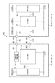
入力回路18の動作は、バンプB1に入力されるデータ信号SD4がHighレベルの場合には、ノードN2にHighレベルである1.5Vを出力する。一方、データ信号SD4がLowレベルの場合には、ノードN2はLowレベルを出力する。
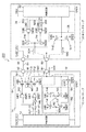
第3の実施例は、第1の実施例に比べて、NMOSトランジスタTr3を形成する必要が無いため、構成が単純であるという利点がある。一方、第1の実施例は、第3実施例に比べて、回路面積を小さくすることができるという利点がある。その理由を、図5を用いて説明する。
12 メモリチップの内部回路
14 メモリチップの出力回路
16 メモリチップの電源電圧供給回路
18 メモリチップの入力回路
20 ロジックチップ
22 ロジックチップの内部回路
24 ロジックチップの出力回路
28 ロジックチップの入力回路
30 STI
SD1,SD2,SD3,SD4,SD5,SD6 データ信号
SV 電圧信号
Vdd1 第1電源電圧(1.5V)を供給する電源線
Vdd2 第2電源電圧(1.0V)を供給する電源線
B1,B2,B3,B4 バンプ
GND1、GND2 接地電位を供給する電源線
Tr MOSトランジスタ
Claims (5)
- 互いに相補的にオンとオフが切り替わる第1および第2トランジスタを有し、第1外部端子へ信号を出力する出力回路と、
第2外部端子にゲート電極が接続された第3トランジスタと、
第1電源供給源と、を有し、
前記第1、第2および第3トランジスタのゲート電極以外の端子に対して、
前記第1トランジスタの一方の端子が前記第1電源供給源と接続され、前記第1トランジスタの他方の端子が前記第3トランジスタの一方の端子と接続され、前記第3トランジスタの他方の端子が前記第2トランジスタの一方の端子および前記第1の外部端子と接続され、前記第2トランジスタの他方の端子が接地電位を供給する電源線と接続されたことを特徴とする半導体チップ。 - 前記出力回路に信号を出力する内部回路をさらに有し、
前記内部回路が前記第1電源電圧供給源により供給される電圧で動作することを特徴とする請求項1に記載の半導体チップ。 - 前記第3トランジスタが、ゲート電極に印加された電圧を前記第3トランジスタの他方の端子に出力することを特徴とする請求項1または2に記載の半導体チップ。
- 前記第3トランジスタのしきい値が実質的に0Vであること、
を特徴とする請求項3に記載の半導体チップ。 - 前記第1および第2トランジスタが3−Stateバッファ回路を構成することを特徴とする請求項1乃至4のいずれか一に記載の半導体チップ。
Priority Applications (5)
| Application Number | Priority Date | Filing Date | Title |
|---|---|---|---|
| JP2005336133A JP4776355B2 (ja) | 2005-11-21 | 2005-11-21 | 半導体チップおよび半導体装置 |
| US11/561,567 US7902873B2 (en) | 2005-11-21 | 2006-11-20 | Semiconductor chip and semiconductor device |
| US13/015,246 US8350593B2 (en) | 2005-11-21 | 2011-01-27 | Semiconductor chip and semiconductor device |
| US13/735,661 US9099330B2 (en) | 2005-11-21 | 2013-01-07 | Semiconductor chip and semiconductor device |
| US14/754,998 US9762244B2 (en) | 2005-11-21 | 2015-06-30 | Semiconductor chip and semiconductor device |
Applications Claiming Priority (1)
| Application Number | Priority Date | Filing Date | Title |
|---|---|---|---|
| JP2005336133A JP4776355B2 (ja) | 2005-11-21 | 2005-11-21 | 半導体チップおよび半導体装置 |
Related Child Applications (2)
| Application Number | Title | Priority Date | Filing Date |
|---|---|---|---|
| JP2011126052A Division JP5202691B2 (ja) | 2011-06-06 | 2011-06-06 | 半導体装置 |
| JP2011126051A Division JP5208249B2 (ja) | 2011-06-06 | 2011-06-06 | 半導体チップ |
Publications (2)
| Publication Number | Publication Date |
|---|---|
| JP2007142968A JP2007142968A (ja) | 2007-06-07 |
| JP4776355B2 true JP4776355B2 (ja) | 2011-09-21 |
Family
ID=38091700
Family Applications (1)
| Application Number | Title | Priority Date | Filing Date |
|---|---|---|---|
| JP2005336133A Expired - Fee Related JP4776355B2 (ja) | 2005-11-21 | 2005-11-21 | 半導体チップおよび半導体装置 |
Country Status (2)
| Country | Link |
|---|---|
| US (4) | US7902873B2 (ja) |
| JP (1) | JP4776355B2 (ja) |
Families Citing this family (3)
| Publication number | Priority date | Publication date | Assignee | Title |
|---|---|---|---|---|
| JP5357510B2 (ja) * | 2008-10-31 | 2013-12-04 | 株式会社日立製作所 | 半導体集積回路装置 |
| US8895327B1 (en) * | 2011-12-09 | 2014-11-25 | Suvolta, Inc. | Tipless transistors, short-tip transistors, and methods and circuits therefor |
| US10164773B2 (en) * | 2016-09-30 | 2018-12-25 | Intel Corporation | Energy-efficient dual-rail keeperless domino datapath circuits |
Family Cites Families (12)
| Publication number | Priority date | Publication date | Assignee | Title |
|---|---|---|---|---|
| JPH09116416A (ja) * | 1995-10-18 | 1997-05-02 | Hitachi Ltd | 入出力バッファ回路 |
| JPH1141082A (ja) * | 1997-07-16 | 1999-02-12 | Sony Corp | 出力バッファ回路 |
| US5966030A (en) * | 1997-08-05 | 1999-10-12 | Lsi Logic Corporation | Output buffer with regulated voltage biasing for driving voltages greater than transistor tolerance |
| US6064229A (en) * | 1998-03-26 | 2000-05-16 | Lucent Technologies Inc. | Voltage translating buffer based on low voltage technology |
| US6147540A (en) * | 1998-08-31 | 2000-11-14 | Motorola Inc. | High voltage input buffer made by a low voltage process and having a self-adjusting trigger point |
| US6130557A (en) * | 1999-04-26 | 2000-10-10 | Ati Technologies, Inc. | Three level pre-buffer voltage level shifting circuit and method |
| US6429686B1 (en) * | 2000-06-16 | 2002-08-06 | Xilinx, Inc. | Output driver circuit using thin and thick gate oxides |
| JP2003133938A (ja) * | 2001-10-26 | 2003-05-09 | Mitsubishi Electric Corp | 出力回路 |
| JP2003218674A (ja) * | 2002-01-17 | 2003-07-31 | Mitsubishi Electric Corp | 半導体集積回路における出力バッファ、入力バッファおよび双方向バッファ |
| JP4587676B2 (ja) | 2004-01-29 | 2010-11-24 | ルネサスエレクトロニクス株式会社 | チップ積層構成の3次元半導体装置 |
| US7173472B2 (en) * | 2004-06-03 | 2007-02-06 | Taiwan Semiconductor Manufacturing Co., Ltd. | Input buffer structure with single gate oxide |
| JP4811852B2 (ja) * | 2005-08-29 | 2011-11-09 | ルネサスエレクトロニクス株式会社 | スイッチング電源と半導体集積回路 |
-
2005
- 2005-11-21 JP JP2005336133A patent/JP4776355B2/ja not_active Expired - Fee Related
-
2006
- 2006-11-20 US US11/561,567 patent/US7902873B2/en active Active
-
2011
- 2011-01-27 US US13/015,246 patent/US8350593B2/en not_active Expired - Fee Related
-
2013
- 2013-01-07 US US13/735,661 patent/US9099330B2/en not_active Expired - Fee Related
-
2015
- 2015-06-30 US US14/754,998 patent/US9762244B2/en not_active Expired - Fee Related
Also Published As
| Publication number | Publication date |
|---|---|
| US20110133803A1 (en) | 2011-06-09 |
| US8350593B2 (en) | 2013-01-08 |
| US9762244B2 (en) | 2017-09-12 |
| US7902873B2 (en) | 2011-03-08 |
| US20070114571A1 (en) | 2007-05-24 |
| JP2007142968A (ja) | 2007-06-07 |
| US20130154706A1 (en) | 2013-06-20 |
| US20150303924A1 (en) | 2015-10-22 |
| US9099330B2 (en) | 2015-08-04 |
Similar Documents
| Publication | Publication Date | Title |
|---|---|---|
| US10692856B2 (en) | Semiconductor integrated circuit device | |
| JP4850387B2 (ja) | 半導体装置 | |
| CN105577145B (zh) | 半导体集成电路器件 | |
| US7969190B2 (en) | Input stage for mixed-voltage-tolerant buffer with reduced leakage | |
| JP2006121654A (ja) | レベル変換回路 | |
| CN101207380B (zh) | 单井电压的电压电平转换器 | |
| KR20080002686A (ko) | 반도체 집적 회로 | |
| JP5143413B2 (ja) | 半導体集積回路 | |
| JP4776355B2 (ja) | 半導体チップおよび半導体装置 | |
| JP2007035672A (ja) | 半導体集積回路装置 | |
| JP2007227625A (ja) | 半導体集積回路及びそのレイアウト設計方法 | |
| US20020043671A1 (en) | Semiconductor integrated circuit having circuit for transmitting input signal | |
| US7215178B2 (en) | MOS type semiconductor integrated circuit device | |
| JP5202691B2 (ja) | 半導体装置 | |
| JP5208249B2 (ja) | 半導体チップ | |
| US6873189B2 (en) | I/O buffer circuit | |
| JP3551926B2 (ja) | バッファ回路 | |
| JP4647143B2 (ja) | 半導体集積回路 | |
| JPS626370B2 (ja) | ||
| JP2008244071A (ja) | Esd保護回路を備えた半導体集積回路 | |
| JP2671808B2 (ja) | インタフェース回路 | |
| US20030183926A1 (en) | Semiconductor device and semiconductor packaging device | |
| JPH098638A (ja) | Cmos入出力バッファ回路 | |
| JPH11176950A (ja) | 半導体集積回路装置 | |
| KR20070021607A (ko) | 액티브 저항의 레이아웃 구조 및 레이아웃 방법 |
Legal Events
| Date | Code | Title | Description |
|---|---|---|---|
| RD01 | Notification of change of attorney |
Free format text: JAPANESE INTERMEDIATE CODE: A7421 Effective date: 20070705 |
|
| A621 | Written request for application examination |
Free format text: JAPANESE INTERMEDIATE CODE: A621 Effective date: 20081017 |
|
| RD01 | Notification of change of attorney |
Free format text: JAPANESE INTERMEDIATE CODE: A7421 Effective date: 20100426 |
|
| A977 | Report on retrieval |
Free format text: JAPANESE INTERMEDIATE CODE: A971007 Effective date: 20110302 |
|
| A131 | Notification of reasons for refusal |
Free format text: JAPANESE INTERMEDIATE CODE: A131 Effective date: 20110405 |
|
| A521 | Request for written amendment filed |
Free format text: JAPANESE INTERMEDIATE CODE: A523 Effective date: 20110606 |
|
| TRDD | Decision of grant or rejection written | ||
| A01 | Written decision to grant a patent or to grant a registration (utility model) |
Free format text: JAPANESE INTERMEDIATE CODE: A01 Effective date: 20110628 |
|
| A01 | Written decision to grant a patent or to grant a registration (utility model) |
Free format text: JAPANESE INTERMEDIATE CODE: A01 |
|
| A61 | First payment of annual fees (during grant procedure) |
Free format text: JAPANESE INTERMEDIATE CODE: A61 Effective date: 20110628 |
|
| R150 | Certificate of patent or registration of utility model |
Ref document number: 4776355 Country of ref document: JP Free format text: JAPANESE INTERMEDIATE CODE: R150 Free format text: JAPANESE INTERMEDIATE CODE: R150 |
|
| FPAY | Renewal fee payment (event date is renewal date of database) |
Free format text: PAYMENT UNTIL: 20140708 Year of fee payment: 3 |
|
| S531 | Written request for registration of change of domicile |
Free format text: JAPANESE INTERMEDIATE CODE: R313531 |
|
| R350 | Written notification of registration of transfer |
Free format text: JAPANESE INTERMEDIATE CODE: R350 |
|
| LAPS | Cancellation because of no payment of annual fees |