JP4780268B2 - 電力半導体モジュール、および電力半導体モジュールの製造方法 - Google Patents
電力半導体モジュール、および電力半導体モジュールの製造方法 Download PDFInfo
- Publication number
- JP4780268B2 JP4780268B2 JP2003500964A JP2003500964A JP4780268B2 JP 4780268 B2 JP4780268 B2 JP 4780268B2 JP 2003500964 A JP2003500964 A JP 2003500964A JP 2003500964 A JP2003500964 A JP 2003500964A JP 4780268 B2 JP4780268 B2 JP 4780268B2
- Authority
- JP
- Japan
- Prior art keywords
- carrier element
- carrier
- module
- module housing
- semiconductor
- Prior art date
- Legal status (The legal status is an assumption and is not a legal conclusion. Google has not performed a legal analysis and makes no representation as to the accuracy of the status listed.)
- Expired - Fee Related
Links
Images

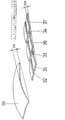

Classifications
-
- H—ELECTRICITY
- H10—SEMICONDUCTOR DEVICES; ELECTRIC SOLID-STATE DEVICES NOT OTHERWISE PROVIDED FOR
- H10W—GENERIC PACKAGES, INTERCONNECTIONS, CONNECTORS OR OTHER CONSTRUCTIONAL DETAILS OF DEVICES COVERED BY CLASS H10
- H10W90/00—Package configurations
-
- H—ELECTRICITY
- H10—SEMICONDUCTOR DEVICES; ELECTRIC SOLID-STATE DEVICES NOT OTHERWISE PROVIDED FOR
- H10W—GENERIC PACKAGES, INTERCONNECTIONS, CONNECTORS OR OTHER CONSTRUCTIONAL DETAILS OF DEVICES COVERED BY CLASS H10
- H10W74/00—Encapsulations, e.g. protective coatings
-
- H—ELECTRICITY
- H10—SEMICONDUCTOR DEVICES; ELECTRIC SOLID-STATE DEVICES NOT OTHERWISE PROVIDED FOR
- H10W—GENERIC PACKAGES, INTERCONNECTIONS, CONNECTORS OR OTHER CONSTRUCTIONAL DETAILS OF DEVICES COVERED BY CLASS H10
- H10W90/00—Package configurations
- H10W90/701—Package configurations characterised by the relative positions of pads or connectors relative to package parts
- H10W90/751—Package configurations characterised by the relative positions of pads or connectors relative to package parts of bond wires
- H10W90/753—Package configurations characterised by the relative positions of pads or connectors relative to package parts of bond wires between laterally-adjacent chips
Landscapes
- Cooling Or The Like Of Semiconductors Or Solid State Devices (AREA)
- Structures Or Materials For Encapsulating Or Coating Semiconductor Devices Or Solid State Devices (AREA)
Applications Claiming Priority (3)
| Application Number | Priority Date | Filing Date | Title |
|---|---|---|---|
| DE10125697.3 | 2001-05-25 | ||
| DE10125697.3A DE10125697B4 (de) | 2001-05-25 | 2001-05-25 | Leistungshalbleitermodul und Verfahren zum Herstellen eines Leistungshalbleitermoduls |
| PCT/EP2002/005520 WO2002097880A2 (fr) | 2001-05-25 | 2002-05-18 | Module a semi-conducteur de puissance et procede pour produire un module a semi-conducteur de puissance |
Publications (2)
| Publication Number | Publication Date |
|---|---|
| JP2004532529A JP2004532529A (ja) | 2004-10-21 |
| JP4780268B2 true JP4780268B2 (ja) | 2011-09-28 |
Family
ID=7686238
Family Applications (1)
| Application Number | Title | Priority Date | Filing Date |
|---|---|---|---|
| JP2003500964A Expired - Fee Related JP4780268B2 (ja) | 2001-05-25 | 2002-05-18 | 電力半導体モジュール、および電力半導体モジュールの製造方法 |
Country Status (3)
| Country | Link |
|---|---|
| JP (1) | JP4780268B2 (fr) |
| DE (1) | DE10125697B4 (fr) |
| WO (1) | WO2002097880A2 (fr) |
Families Citing this family (3)
| Publication number | Priority date | Publication date | Assignee | Title |
|---|---|---|---|---|
| WO2003071601A2 (fr) * | 2002-02-18 | 2003-08-28 | Infineon Technologies Ag | Module de circuit et procede de fabrication |
| DE102005061772B4 (de) * | 2005-12-23 | 2017-09-07 | Danfoss Silicon Power Gmbh | Leistungshalbleitermodul |
| JP5565147B2 (ja) | 2010-06-30 | 2014-08-06 | 株式会社デンソー | 半導体モジュールの製造方法 |
Family Cites Families (14)
| Publication number | Priority date | Publication date | Assignee | Title |
|---|---|---|---|---|
| JPS5710951A (en) * | 1980-06-25 | 1982-01-20 | Rohm Co Ltd | Semiconductor device |
| JP2582013B2 (ja) * | 1991-02-08 | 1997-02-19 | 株式会社東芝 | 樹脂封止型半導体装置及びその製造方法 |
| DE3508456C2 (de) * | 1985-03-09 | 1987-01-08 | Brown, Boveri & Cie Ag, 6800 Mannheim | Leistungshalbleitermodul und Verfahren zur Herstellung eines solchen Moduls |
| KR910001419B1 (ko) * | 1987-03-31 | 1991-03-05 | 가부시키가이샤 도시바 | 수지봉합형 집적회로장치 |
| IT1221585B (it) * | 1987-05-18 | 1990-07-12 | S G S Microelettronica Spa Ora | Circuito modulare a piu' piastrine a semiconduttore in capsulato in resina,e relativo procedimento di fabbrivazione |
| JPH02201949A (ja) | 1989-01-30 | 1990-08-10 | Toshiba Corp | 半導体装置 |
| US5075759A (en) | 1989-07-21 | 1991-12-24 | Motorola, Inc. | Surface mounting semiconductor device and method |
| DE3940933C2 (de) | 1989-12-12 | 1996-08-01 | Eupec Gmbh & Co Kg | Verfahren zum Verformen einer Basisplatte für Halbleitermodule und Vorrichtung zum Durchführen des Verfahrens |
| US5245216A (en) * | 1990-09-11 | 1993-09-14 | Kabushiki Kaisha Toshiba | Plastic-molded type semiconductor device |
| US5194933A (en) | 1990-10-05 | 1993-03-16 | Fuji Electric Co., Ltd. | Semiconductor device using insulation coated metal substrate |
| JPH06151685A (ja) * | 1992-11-04 | 1994-05-31 | Mitsubishi Electric Corp | Mcp半導体装置 |
| JP3206717B2 (ja) | 1996-04-02 | 2001-09-10 | 富士電機株式会社 | 電力用半導体モジュール |
| US6404065B1 (en) | 1998-07-31 | 2002-06-11 | I-Xys Corporation | Electrically isolated power semiconductor package |
| EP1122778A3 (fr) * | 2000-01-31 | 2004-04-07 | Sanyo Electric Co., Ltd. | Dispositif de circuit et son procédé de fabrication |
-
2001
- 2001-05-25 DE DE10125697.3A patent/DE10125697B4/de not_active Expired - Fee Related
-
2002
- 2002-05-18 JP JP2003500964A patent/JP4780268B2/ja not_active Expired - Fee Related
- 2002-05-18 WO PCT/EP2002/005520 patent/WO2002097880A2/fr not_active Ceased
Also Published As
| Publication number | Publication date |
|---|---|
| WO2002097880A2 (fr) | 2002-12-05 |
| DE10125697B4 (de) | 2019-01-03 |
| DE10125697A1 (de) | 2002-12-05 |
| WO2002097880A3 (fr) | 2003-09-25 |
| JP2004532529A (ja) | 2004-10-21 |
Similar Documents
| Publication | Publication Date | Title |
|---|---|---|
| US4731701A (en) | Integrated circuit package with thermal path layers incorporating staggered thermal vias | |
| KR0145275B1 (ko) | 회로장치 | |
| TW405196B (en) | Segmented architecture for wafer test & burn-in | |
| US7615872B2 (en) | Semiconductor device | |
| US20040233649A1 (en) | Electronic chip and electronic chip assembly | |
| JP2009532912A (ja) | 一体型スルーホール熱放散ピンを有するモールドされた半導体パッケージ | |
| US5233131A (en) | Integrated circuit die-to-leadframe interconnect assembly system | |
| US5596227A (en) | Ball grid array type semiconductor device | |
| RU2190284C2 (ru) | Двусторонний электронный прибор | |
| JPH05326808A (ja) | 電子部品搭載用基板およびこれを用いた半導体装置 | |
| JP2005509278A (ja) | 電力半導体モジュール | |
| JP4780268B2 (ja) | 電力半導体モジュール、および電力半導体モジュールの製造方法 | |
| US5886396A (en) | Leadframe assembly for conducting thermal energy from a semiconductor die disposed in a package | |
| JPH04299851A (ja) | 半導体装置用リードフレーム | |
| US5736234A (en) | Multilayer printed circuit board having latticed films on an interconnection layer | |
| KR100237895B1 (ko) | 저가 수지 몰드 반도체 장치 | |
| JPH06291230A (ja) | 複合半導体装置の製造方法 | |
| JP3910694B2 (ja) | 外部端子付半導体素子の製造方法 | |
| JP3540210B2 (ja) | Ccdモールドパッケージの構造 | |
| US20060141667A1 (en) | Bare die socket | |
| JP2004153243A (ja) | 電力用半導体装置 | |
| JPH06169109A (ja) | 熱電素子 | |
| JP2007035913A (ja) | 半導体装置 | |
| JP4641635B2 (ja) | ヒートシンク集合体 | |
| JPH04237154A (ja) | 半導体パッケージ |
Legal Events
| Date | Code | Title | Description |
|---|---|---|---|
| A977 | Report on retrieval |
Free format text: JAPANESE INTERMEDIATE CODE: A971007 Effective date: 20061129 |
|
| A131 | Notification of reasons for refusal |
Free format text: JAPANESE INTERMEDIATE CODE: A131 Effective date: 20061205 |
|
| A601 | Written request for extension of time |
Free format text: JAPANESE INTERMEDIATE CODE: A601 Effective date: 20070221 |
|
| RD02 | Notification of acceptance of power of attorney |
Free format text: JAPANESE INTERMEDIATE CODE: A7422 Effective date: 20070221 |
|
| A602 | Written permission of extension of time |
Free format text: JAPANESE INTERMEDIATE CODE: A602 Effective date: 20070314 |
|
| A521 | Request for written amendment filed |
Free format text: JAPANESE INTERMEDIATE CODE: A523 Effective date: 20070518 |
|
| A131 | Notification of reasons for refusal |
Free format text: JAPANESE INTERMEDIATE CODE: A131 Effective date: 20080401 |
|
| A601 | Written request for extension of time |
Free format text: JAPANESE INTERMEDIATE CODE: A601 Effective date: 20080627 |
|
| A602 | Written permission of extension of time |
Free format text: JAPANESE INTERMEDIATE CODE: A602 Effective date: 20080704 |
|
| A521 | Request for written amendment filed |
Free format text: JAPANESE INTERMEDIATE CODE: A523 Effective date: 20080728 |
|
| A02 | Decision of refusal |
Free format text: JAPANESE INTERMEDIATE CODE: A02 Effective date: 20081202 |
|
| A521 | Request for written amendment filed |
Free format text: JAPANESE INTERMEDIATE CODE: A523 Effective date: 20090331 |
|
| A911 | Transfer to examiner for re-examination before appeal (zenchi) |
Free format text: JAPANESE INTERMEDIATE CODE: A911 Effective date: 20090417 |
|
| A912 | Re-examination (zenchi) completed and case transferred to appeal board |
Free format text: JAPANESE INTERMEDIATE CODE: A912 Effective date: 20090619 |
|
| A521 | Request for written amendment filed |
Free format text: JAPANESE INTERMEDIATE CODE: A523 Effective date: 20110513 |
|
| A01 | Written decision to grant a patent or to grant a registration (utility model) |
Free format text: JAPANESE INTERMEDIATE CODE: A01 |
|
| A711 | Notification of change in applicant |
Free format text: JAPANESE INTERMEDIATE CODE: A712 Effective date: 20110621 |
|
| A61 | First payment of annual fees (during grant procedure) |
Free format text: JAPANESE INTERMEDIATE CODE: A61 Effective date: 20110621 |
|
| FPAY | Renewal fee payment (event date is renewal date of database) |
Free format text: PAYMENT UNTIL: 20140715 Year of fee payment: 3 |
|
| R150 | Certificate of patent or registration of utility model |
Free format text: JAPANESE INTERMEDIATE CODE: R150 Ref document number: 4780268 Country of ref document: JP Free format text: JAPANESE INTERMEDIATE CODE: R150 |
|
| R250 | Receipt of annual fees |
Free format text: JAPANESE INTERMEDIATE CODE: R250 |
|
| R250 | Receipt of annual fees |
Free format text: JAPANESE INTERMEDIATE CODE: R250 |
|
| R250 | Receipt of annual fees |
Free format text: JAPANESE INTERMEDIATE CODE: R250 |
|
| R250 | Receipt of annual fees |
Free format text: JAPANESE INTERMEDIATE CODE: R250 |
|
| R250 | Receipt of annual fees |
Free format text: JAPANESE INTERMEDIATE CODE: R250 |
|
| R250 | Receipt of annual fees |
Free format text: JAPANESE INTERMEDIATE CODE: R250 |
|
| LAPS | Cancellation because of no payment of annual fees |