JP4786202B2 - 半導体発光素子 - Google Patents
半導体発光素子 Download PDFInfo
- Publication number
- JP4786202B2 JP4786202B2 JP2005061348A JP2005061348A JP4786202B2 JP 4786202 B2 JP4786202 B2 JP 4786202B2 JP 2005061348 A JP2005061348 A JP 2005061348A JP 2005061348 A JP2005061348 A JP 2005061348A JP 4786202 B2 JP4786202 B2 JP 4786202B2
- Authority
- JP
- Japan
- Prior art keywords
- layer
- graded
- energy band
- band gap
- semiconductor light
- Prior art date
- Legal status (The legal status is an assumption and is not a legal conclusion. Google has not performed a legal analysis and makes no representation as to the accuracy of the status listed.)
- Expired - Lifetime
Links
Images





Landscapes
- Led Devices (AREA)
Description
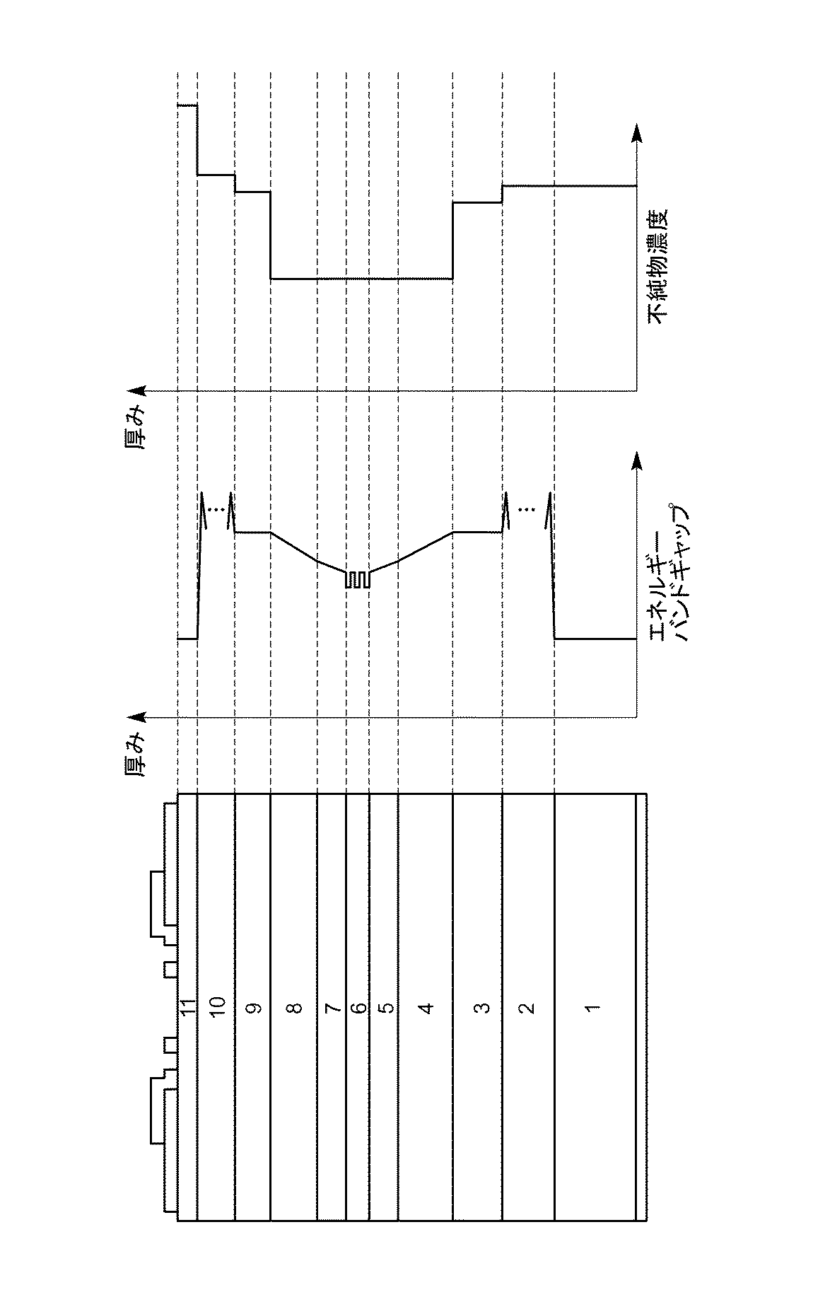
C4=C0+C×(d−D)
エネルギーバンドギャップE=1.89〜1.92eV
距離D=25nm〜70nm
(比較例1)
(比較例2)
(1)比較例1の半導体発光素子の応答特性の遮断周波数は90MHz程度であったが、実施の形態の半導体発光素子の応答特性の遮断周波数(発光に変化のない周波数から3dB発光が減衰する周波数)は100MHzとなり、10%程度の応答速度の改善が見られた。
(2)実施の形態の半導体発光素子の光出力低下は殆ど認められなかった。
(3)発光に必要な順方向電圧が比較例1では2.07Vであったが、実施の形態の半導体発光素子を用いた場合、発光に必要な順方向電圧は2.02Vとなり、0.05Vも低下した。
Claims (4)
- 第1のクラッド層と、
前記第1のクラッド層上に形成された第1のグレーデッド層と、
前記第1のグレーデッド層上に形成された活性層と、
前記活性層上に形成された第2のグレーデッド層と、
前記第2のグレーデッド層上に形成された第2のクラッド層と、を備え、
前記第1のクラッド層は前記活性層よりもエネルギーバンドギャップが大きく、
前記第2のクラッド層は前記活性層よりもエネルギーバンドギャップが大きく、
前記第1のグレーデッド層は、前記活性層と前記第1のクラッド層との間のエネルギーバンドギャップを有してエネルギーバンドギャップが、前記第1のクラッド層のエネルギーバンドギャップになるまで、連続的に変化し、
前記第2のグレーデッド層は、前記活性層と前記第2のクラッド層との間のエネルギーバンドギャップを有してエネルギーバンドギャップが、前記第2のクラッド層のエネルギーバンドギャップになるまで、連続的に変化した半導体発光素子において、
前記第1及び第2のクラッド層は高キャリア濃度を有しており、
前記第1及び/又は第2のグレーデッド層は、それぞれに隣接する前記クラッド層との境界近傍において、キャリア濃度が前記クラッド層に向かうに従って連続的に増加していることを特徴とする半導体発光素子。 - 前記第1のクラッド層、前記第1のグレーデッド層、前記第2のグレーデッド層及び前記第2のクラッド層は、それぞれAlGaInPからなることを特徴とする請求項1に記載の半導体発光素子。
- 前記活性層は、GaInP及びAlGaInPを交互に積層してなる多重量子井戸構造を有することを特徴とする請求項2に記載の半導体発光素子。
- 前記第1及び/又は第2のグレーデッド層は、それぞれに隣接する前記クラッド層との界面において、キャリア濃度及び組成が前記クラッド層と等しく設定されることを特徴とする請求項1に記載の半導体発光素子。
Priority Applications (1)
| Application Number | Priority Date | Filing Date | Title |
|---|---|---|---|
| JP2005061348A JP4786202B2 (ja) | 2005-03-04 | 2005-03-04 | 半導体発光素子 |
Applications Claiming Priority (1)
| Application Number | Priority Date | Filing Date | Title |
|---|---|---|---|
| JP2005061348A JP4786202B2 (ja) | 2005-03-04 | 2005-03-04 | 半導体発光素子 |
Publications (2)
| Publication Number | Publication Date |
|---|---|
| JP2006245441A JP2006245441A (ja) | 2006-09-14 |
| JP4786202B2 true JP4786202B2 (ja) | 2011-10-05 |
Family
ID=37051501
Family Applications (1)
| Application Number | Title | Priority Date | Filing Date |
|---|---|---|---|
| JP2005061348A Expired - Lifetime JP4786202B2 (ja) | 2005-03-04 | 2005-03-04 | 半導体発光素子 |
Country Status (1)
| Country | Link |
|---|---|
| JP (1) | JP4786202B2 (ja) |
Families Citing this family (2)
| Publication number | Priority date | Publication date | Assignee | Title |
|---|---|---|---|---|
| US20110298005A1 (en) * | 2007-10-12 | 2011-12-08 | Lattice Power (Jiangxi) Corporation | Method for fabricating an n-type semiconductor material using silane as a precursor |
| US8507929B2 (en) * | 2008-06-16 | 2013-08-13 | Koninklijke Philips Electronics N.V. | Semiconductor light emitting device including graded region |
Family Cites Families (5)
| Publication number | Priority date | Publication date | Assignee | Title |
|---|---|---|---|---|
| JPH06177484A (ja) * | 1992-12-10 | 1994-06-24 | Sony Corp | 発光素子 |
| JP3024484B2 (ja) * | 1994-07-01 | 2000-03-21 | サンケン電気株式会社 | 半導体発光素子 |
| JPH11340580A (ja) * | 1997-07-30 | 1999-12-10 | Fujitsu Ltd | 半導体レーザ、半導体発光素子、及び、その製造方法 |
| JP3552642B2 (ja) * | 2000-04-13 | 2004-08-11 | 日本電気株式会社 | 半導体発光素子及びその製造方法 |
| JP2004228212A (ja) * | 2003-01-21 | 2004-08-12 | Sharp Corp | 酸化物半導体発光素子 |
-
2005
- 2005-03-04 JP JP2005061348A patent/JP4786202B2/ja not_active Expired - Lifetime
Also Published As
| Publication number | Publication date |
|---|---|
| JP2006245441A (ja) | 2006-09-14 |
Similar Documents
| Publication | Publication Date | Title |
|---|---|---|
| JP4954536B2 (ja) | 窒化物半導体発光素子 | |
| TWI742714B (zh) | 半導體雷射二極體 | |
| JP2011171369A (ja) | 半導体発光素子 | |
| US20090146163A1 (en) | High brightness light emitting diode structure | |
| JP5485905B2 (ja) | 半導体レーザ素子 | |
| JP3872398B2 (ja) | 発光素子の製造方法及び発光素子 | |
| EP2919282B1 (en) | Nitride semiconductor stacked body and semiconductor light emitting device comprising the same | |
| CN101180743A (zh) | 氮化物半导体发光元件 | |
| KR20130096991A (ko) | 자외선 발광소자 | |
| JP5935178B2 (ja) | 半導体発光素子 | |
| JP4483615B2 (ja) | 半導体発光素子用エピタキシャルウェハ及び半導体発光素子 | |
| KR100905877B1 (ko) | 질화물 반도체 소자 | |
| US20230096932A1 (en) | Surface emitting laser | |
| JP2017045798A (ja) | 窒化物半導体積層体および半導体発光素子 | |
| JP4786202B2 (ja) | 半導体発光素子 | |
| CN1925180A (zh) | 半导体发光元件用外延晶片、其制造方法及半导体发光元件 | |
| JP2013069795A (ja) | 半導体発光素子 | |
| JP7373435B2 (ja) | 半導体発光素子 | |
| JP4884826B2 (ja) | 半導体発光素子 | |
| JPH11220172A (ja) | 窒化ガリウム系化合物半導体発光素子 | |
| JP5337862B2 (ja) | 半導体発光素子 | |
| WO2021172171A1 (ja) | レーザ素子 | |
| JP5150099B2 (ja) | 発光半導体素子 | |
| JP5554387B2 (ja) | 半導体発光素子 | |
| CN1705143A (zh) | 半导体发光器件用外延片和半导体发光器件 |
Legal Events
| Date | Code | Title | Description |
|---|---|---|---|
| A621 | Written request for application examination |
Free format text: JAPANESE INTERMEDIATE CODE: A621 Effective date: 20080222 |
|
| A131 | Notification of reasons for refusal |
Free format text: JAPANESE INTERMEDIATE CODE: A131 Effective date: 20100914 |
|
| A977 | Report on retrieval |
Free format text: JAPANESE INTERMEDIATE CODE: A971007 Effective date: 20100914 |
|
| A521 | Request for written amendment filed |
Free format text: JAPANESE INTERMEDIATE CODE: A523 Effective date: 20101115 |
|
| TRDD | Decision of grant or rejection written | ||
| A01 | Written decision to grant a patent or to grant a registration (utility model) |
Free format text: JAPANESE INTERMEDIATE CODE: A01 Effective date: 20110712 |
|
| A01 | Written decision to grant a patent or to grant a registration (utility model) |
Free format text: JAPANESE INTERMEDIATE CODE: A01 |
|
| A61 | First payment of annual fees (during grant procedure) |
Free format text: JAPANESE INTERMEDIATE CODE: A61 Effective date: 20110713 |
|
| R150 | Certificate of patent or registration of utility model |
Free format text: JAPANESE INTERMEDIATE CODE: R150 Ref document number: 4786202 Country of ref document: JP Free format text: JAPANESE INTERMEDIATE CODE: R150 |
|
| FPAY | Renewal fee payment (event date is renewal date of database) |
Free format text: PAYMENT UNTIL: 20140722 Year of fee payment: 3 |
|
| R250 | Receipt of annual fees |
Free format text: JAPANESE INTERMEDIATE CODE: R250 |
|
| EXPY | Cancellation because of completion of term |