JP4801848B2 - Liquid crystal display - Google Patents
Liquid crystal display Download PDFInfo
- Publication number
- JP4801848B2 JP4801848B2 JP2001189233A JP2001189233A JP4801848B2 JP 4801848 B2 JP4801848 B2 JP 4801848B2 JP 2001189233 A JP2001189233 A JP 2001189233A JP 2001189233 A JP2001189233 A JP 2001189233A JP 4801848 B2 JP4801848 B2 JP 4801848B2
- Authority
- JP
- Japan
- Prior art keywords
- driving circuit
- signal
- line driving
- liquid crystal
- scanning
- Prior art date
- Legal status (The legal status is an assumption and is not a legal conclusion. Google has not performed a legal analysis and makes no representation as to the accuracy of the status listed.)
- Expired - Fee Related
Links
Images




Landscapes
- Liquid Crystal (AREA)
- Liquid Crystal Display Device Control (AREA)
- Control Of Indicators Other Than Cathode Ray Tubes (AREA)
- Devices For Indicating Variable Information By Combining Individual Elements (AREA)
Description
【0001】
【発明の属する技術分野】
本発明は、アクティブマトリクス方式の液晶表示装置に関し、より詳しくは実用性を高めつつ信号線駆動回路および走査線駆動回路の信号振幅を低減するための駆動方法の改良に関する。
【0002】
【従来の技術】
アクティブマトリクス方式の液晶表示装置において、表示信号の最大振幅の低減、内部直流電圧(寄生容量)による影響の抑制等のため、液晶の保持特性を高めるための保持容量を前段走査線と画素電極の間に設け、ここから液晶にバイアス電圧を印加する対向一定容量結合駆動方法と呼ばれる方法がある(例えば日経BP社 フラットパネル・ディスプレイ‘93 P128〜P131)。
【0003】
しかしながら、この方法によると、一方で走査信号の振幅を大きくする必要がある。そこで、特開平10−39277号公報には、走査線と独立した補助容量を設け、この補助容量にパルス状波形を加えて液晶にバイアス電位を加える方法が提案されている。
【0004】
同公報による表示装置の構成の概略を図17に、1画素の電気的構成図を図2に示す。表示領域20には複数の信号線1が平行に配されていて、さらに複数の走査線2が信号線1に直交するように配されている。信号線1と走査線2の各交点の近傍にはスイッチング素子3が配されている。スイッチング素子3は走査線駆動回路10より走査線2を介して入力した走査信号により信号線1と画素電極4との接続をオン・オフ制御する。液晶層7は画素電極4と対向電極11との間に形成された電界により駆動する。複数の共通電極線5が走査線2と対をなしてそれと略平行に配される。画素電極4と共通電極線5の間には保持容量6が形成される。
【0005】
信号線駆動回路9は、フレーム期間ごとに対向電極11の電位Vcomに対して論理極性が反転したパルス信号を信号線1のそれぞれに出力する。
【0006】
走査線駆動回路10は、VoffおよびVonの2値を発生するバッファとシフトレジスタとを備え、スタート信号Vstとクロック信号Vclkに基づいて走査線2を駆動するための走査信号のVoffまたはVonを出力する。
【0007】
共通電極線駆動回路12はスイッチを備え、入力された信号VstとVclkに基づいて信号源(図示せず)より入力したVe(−)、Ve、Ve(+)の3値のいずれかを共通電極線5に出力する。
【0008】
ここで、スイッチング素子3は、たとえば非晶質シリコン(a−Si)、多結晶ポリシリコン(p−Si)等を用いた薄膜トランジスタである。また、反射型や投射型のパネルには、広くICに用いられる単結晶シリコン(c−Si)を用いたものも多い。
【0009】
これらのデバイスにはその構造上、走査線2と画素電極4の間に寄生容量すなわちゲート−ドレイン間容量8が形成されるため、走査線駆動回路10からの走査信号がVonからVoffに変化する時に、画素電極4の電位を負側にシフトする。
【0010】
そこで、同公報では、この画素電極4の電位の降下を補償するために、共通電極線5の電位を変化させている。
【0011】
この装置の駆動方法を各電位の動作波形を示す図18を用いて説明する。
【0012】
走査線駆動回路10は、1フレームごとに各走査線2に向けてそれに接続されたスイッチング素子3をオンにするための信号を出力する。走査線2の電位はVoffに維持されながら、その水平走査期間だけVonになる。したがって、スイッチング素子3はその期間だけオンになり、画素電極4と信号線1が電気的に接続される。
【0013】
図中H1で示す水平走査期間においては、画素電極4の電位は低下して信号線1の電位Vs(−)と等しくなる。このときの信号線1の対向電極11に対する論理極性は負である。
【0014】
ここで、期間H1中にVeに維持されていた共通電極線5の電位をVe(+)に上昇させる。期間H1が経過して走査線電位がVoffに低下した瞬間、ゲート−ドレイン間容量8の影響により、画素電極4の電位はわずかに負にシフトする。ここで、ゲート−ドレイン間容量8は液晶層7の容量と保持容量6の総和よりも一桁小さい。
【0015】
期間H1の経過後、共通電極線5の電位をVe(+)からVeに下げる。これにより、画素電極4の電位はほぼこの電位差分負にシフトする。水平走査期間H2に至るまでは、スイッチング素子3がオフであるために画素電極4の電位は維持される。
【0016】
期間H2では、信号線1の論理極性は対向電極11に対して正であって、画素電極4の電位は上昇して信号線1の電位Vs(+)と等しくなる。期間H2中に共通電極線5の電位をVeからVe(−)に下げる。期間H2が経過して走査線2の電位がVoffに低下した瞬間、ゲート−ドレイン間容量8の影響により、画素電極4の電位はわずかに負にシフトする。期間H2の経過後、共通電極線5の電位をVe(−)からVeに上げる。これにより、画素電極4の電位はほぼこの電位差分正にシフトする。
【0017】
上記のように、対向電極電位Vcomに対する論理極性が異なる画像信号が交互に繰り返し画素電極4に入力する。
【0018】
この方法によると、画素電極4の電位の振幅を画像信号の振幅よりも大きくすることができる。
【0019】
【発明が解決しようとする課題】
しかしながら、共通電極線5の振幅がVe(+)とVe(−)の絶対値の和になり、画像信号の振幅よりも大きくなっていた。
【0020】
このため、共通電極線駆動回路には高耐圧の素子が必要となり、機器の小型化や低価格化を妨げる要因となる。また、電池を用いる携帯機器などにおいては、高電圧の生成は電源回路そのものにとっても効率が悪く、電池駆動時間を短縮する原因になりうる。
【0021】
本発明は、上記課題を解決するためのものであり、機器の小型化および低価格化に対応可能でありかつ消費電力の少ないアクティブマトリクス方式の液晶表示装置を提供することを目的とする。
【0022】
【課題を解決するための手段】
本発明の液晶表示装置は、互いに平行に配された複数の信号線、前記信号線と直交する複数の走査線、前記信号線および走査線に囲まれた領域のそれぞれに形成された画素電極、前記走査線より入力した走査信号に基づいて前記画素電極のそれぞれと前記信号線との接続を制御する複数のスイッチング素子、および前記走査線と対をなして前記走査線と略平行に配され、前記画素電極との間に保持容量を形成する共通電極を備えた第一の基板と、前記第一の基板と対向して配された第二の基板と、前記第一および第二の基板の間に挟持された液晶層と、前記画素電極との間に前記液晶層を駆動するための電界を形成するために前記第一または第二の基板に配された対向電極と、前記信号線およびスイッチング素子を介して前記画素電極に画像信号を出力する信号線駆動回路と、前記走査線を介して前記スイッチング素子に前記走査信号を出力する走査線駆動回路と、前記画像信号の論理極性に対応して前記共通電極線に2レベルの変調信号を出力し、前記変調信号は前記走査線がスイッチング素子をオフした後、1乃至Nライン後に変調セットタイミングを有し、前記走査線がスイッチング素子をオフする前1乃至Mライン以前にレベル変更のためのリセットタイミングを有し、N+Mは全ライン数の10%以下で、前記リセットタイミングから前記変調セットタイミングまでの時間は前記走査線が前記スイッチング素子をオンしている期間を含み、前記変調信号の振幅は2レベルのうちの絶対値の大きい方であり3値の電圧からなる共通電極線駆動回路とを具備する。
【0023】
本発明では変調信号の振幅が2レベルあるため、画素電極の電位を対向電極電位に対して任意に設定でき、かつ、変調信号の振幅が小さいため、高耐圧の素子を使用しないで回路を構成できる。
【0024】
本発明の好ましい態様において、走査線駆動回路および共通電極線駆動回路が第一の基板上の表示領域に対して同一の側に配され、両回路に入力される信号の一部は同一の信号源から出力される。基板の面積に対して表示領域を大きくとることができる。
【0025】
本発明の他の好ましい態様において、走査線駆動回路の一部および共通電極線駆動回路の一部が同一のIC基板上に形成される。
【0026】
本発明の他の好ましい態様において、信号線駆動回路の一部および共通電極線駆動回路の一部が同一のIC基板上に形成される。基板上の非表示領域を小さくすることができる。
【0027】
本発明のほかの好ましい態様において、画素電極が反射面を有する。共通電極線の幅を大きくすることができるため、表示に影響を与えずに充分な保持容量を確保することができる。
【0028】
本発明の他の好ましい態様において、走査線駆動回路および共通電極線駆動回路が多結晶、非結晶、または単結晶のシリコン半導体を具備する。より好ましくは、スイッチング素子が、走査線駆動回路および共通電極線駆動回路内のシリコン半導体と同じ材料を含む。これらシリコン半導体に同じ材料を用いることで、同一のプロセスにおいてこれらを形成することができる。
【0029】
本発明のさらに他の液晶表示装置は、互いに平行に配された複数の信号線、前記信号線と直交する複数の走査線、前記信号線および走査線に囲まれた領域のそれぞれに形成された画素電極、前記走査線より入力した走査信号に基づいて前記画素電極のそれぞれと前記信号線との接続を制御する複数のスイッチング素子、および前記走査線と対をなして前記走査線と略平行に配され、前記画素電極との間に保持容量を形成する共通電極を備えた第一の基板と、前記第一の基板と対向して配された第二の基板と、前記第一および第二の基板の間に挟持された液晶層と、前記画素電極との間に前記液晶層を駆動するための電界を形成するために前記第一または第二の基板に配された対向電極と、前記信号線およびスイッチング素子を介して前記画素電極に画像信号を出力する信号線駆動回路と、前記走査線を介して前記スイッチング素子に前記走査信号を出力する走査線駆動回路と、前記画像信号の論理極性に対応して前記共通電極線に2レベルの変調信号を出力し、前記変調信号は前記走査線がスイッチング素子をオフした後、1乃至Nライン後に変調セットタイミングを有し、前記走査線がスイッチング素子をオフする前1乃至Mライン以前にレベル変更のためのリセットタイミングを有し、N+Mは全ライン数の10%以下で、前記リセットタイミングから前記変調セットタイミングまでの時間は前記走査線が前記スイッチング素子をオンしている期間を含み、前記変調信号の振幅は2レベルのうちの絶対値の大きい方であり4値の電圧からなる共通電極線駆動回路とを有する。
【0030】
2レベルの変調信号を4値の電圧で生成するため、変調信号の電圧設定に自由度があり、さらに振幅は変調レベルの大きい方なので、高耐圧素子を使用せず、小規模な回路で低電力で実現できる。
【0031】
本発明のさらに他の液晶表示装置は、互いに平行に配された複数の信号線、前記信号線と直交する複数の走査線、前記信号線および走査線に囲まれた領域のそれぞれに形成された画素電極、前記走査線より入力した走査信号に基づいて前記画素電極のそれぞれと前記信号線との接続を制御する複数のスイッチング素子、および前記走査線と対をなして前記走査線と略平行に配され、前記画素電極との間に保持容量を形成する共通電極を備えた第一の基板と、前記第一の基板と対向して配された第二の基板と、前記第一および第二の基板の間に挟持された液晶層と、前記画素電極との間に前記液晶層を駆動するための電界を形成するために前記第一または第二の基板に配された対向電極と、前記信号線およびスイッチング素子を介して前記画素電極に画像信号を出力する信号線駆動回路と、前記画像信号の電位を決める電位発生回路と、前記走査線を介して前記スイッチング素子に前記走査信号を出力する走査線駆動回路と、前記画像信号の論理極性に対応して前記共通電極線に2レベルの変調信号を出力し、前記変調信号は前記走査線がスイッチング素子をオフした後、1乃至Nライン後に変調セットタイミングを有し、前記走査線がスイッチング素子をオフする前1乃至Mライン以前にレベル変更のためのリセットタイミングを有し、N+Mは全ライン数の10%以下で、前記リセットタイミングから前記変調セットタイミングまでの時間は前記走査線が前記スイッチング素子をオンしている期間を含み、前記変調信号の振幅は2レベルのうちの絶対値の大きい方である共通電極線駆動回路とを具備し、前記共通線駆動回路が使用する電圧の一部と前記電位発生回路が使用する電圧の一部とを共用する。液晶表示装置の駆動回路全体の中で電圧を生成する回路を共用することで、新たな電圧生成のための静的電力の増加を押さえ、回路規模を縮小することができる。
【0032】
本発明のさらに他の液晶表示装置は、互いに平行に配された複数の信号線、前記信号線と直交する複数の走査線、前記信号線および走査線に囲まれた領域のそれぞれに形成された画素電極、前記走査線より入力した走査信号に基づいて前記画素電極のそれぞれと前記信号線との接続を制御する複数のスイッチング素子、および前記走査線と対をなして前記走査線と略平行に配され、前記画素電極との間に保持容量を形成する共通電極を備えた第一の基板と、前記第一の基板と対向して配された第二の基板と、前記第一および第二の基板の間に挟持された液晶層と、前記画素電極との間に前記液晶層を駆動するための電界を形成するために前記第一または第二の基板に配された対向電極と、前記信号線およびスイッチング素子を介して前記画素電極に画像信号を出力する信号線駆動回路と、前記走査線を介して前記スイッチング素子に前記走査信号を出力する走査線駆動回路と、前記画像信号の論理極性に対応して前記共通電極線に2レベルの変調信号を出力し、前記変調信号は前記走査線がスイッチング素子をオフした後、1乃至Nライン後に変調セットタイミングを有し、前記走査線がスイッチング素子をオフする前1乃至Mライン以前にレベル変更のためのリセットタイミングを有し、N+Mは全ライン数の10%以下で、前記リセットタイミングから前記変調セットタイミングまでの時間は前記走査線が前記スイッチング素子をオンしている期間を含み、前記変調信号の振幅は2レベルのうちの絶対値の大きい方である共通電極線駆動回路とを具備し、前記共通線駆動回路が使用する電圧の一部と前記対向電極電位とを共用する。液晶表示装置の駆動回路全体の中で電圧を生成する回路を共用することで、新たな電圧生成のための静的電力の増加を押さえ、回路規模を縮小することができる。
【0033】
本発明のさらに他の液晶表示装置は、互いに平行に配された複数の信号線、前記信号線と直交する複数の走査線、前記信号線および走査線に囲まれた領域のそれぞれに形成された画素電極、前記走査線より入力した走査信号に基づいて前記画素電極のそれぞれと前記信号線との接続を制御する複数のスイッチング素子、および前記走査線と対をなして前記走査線と略平行に配され、前記画素電極との間に保持容量を形成する共通電極を備えた第一の基板と、前記第一の基板と対向して配された第二の基板と、前記第一および第二の基板の間に挟持された液晶層と、前記画素電極との間に前記液晶層を駆動するための電界を形成するために前記第一または第二の基板に配された対向電極と、前記信号線およびスイッチング素子を介して前記画素電極に画像信号を出力する信号線駆動回路と、前記走査線を介して前記スイッチング素子に前記走査信号を出力する走査線駆動回路と、前記画像信号の論理極性に対応して前記共通電極線に2レベルの変調信号を出力し、前記変調信号は前記走査線がスイッチング素子をオフした後、1乃至Nライン後に変調セットタイミングを有し、前記走査線がスイッチング素子をオフする前1乃至Mライン以前にレベル変更のためのリセットタイミングを有し、N+Mは全ライン数の10%以下で、前記リセットタイミングから前記変調セットタイミングまでの時間は前記走査線が前記スイッチング素子をオンしている期間を含み、前記変調信号の振幅は2レベルのうちの絶対値の大きい方で、液晶表示装置としての輝度を変更するための変調信号振幅調整機能を有する共通電極線駆動回路とを有する。信号線の電圧振幅を大きくすると、信号線は容量性負荷が大きいため消費電力がかなり増大するが、信号線振幅を変化させずに変調信号振幅を変化させれば、電力の増大は小さいまま、輝度を変更することができる。
【0034】
本発明のさらに他の液晶表示装置は、互いに平行に配された複数の信号線、前記信号線と直交する複数の走査線、前記信号線および走査線に囲まれた領域のそれぞれに形成された画素電極、前記走査線より入力した走査信号に基づいて前記画素電極のそれぞれと前記信号線との接続を制御する複数のスイッチング素子、および前記走査線と対をなして前記走査線と略平行に配され、前記画素電極との間に保持容量を形成する共通電極を備えた第一の基板と、前記第一の基板と対向して配された第二の基板と、前記第一および第二の基板の間に挟持された液晶層と、前記画素電極との間に前記液晶層を駆動するための電界を形成するために前記第一または第二の基板に配された対向電極と、前記信号線およびスイッチング素子を介して前記画素電極に画像信号を出力する信号線駆動回路と、前記走査線を介して前記スイッチング素子に前記走査信号を出力する走査線駆動回路と、前記画像信号の論理極性に対応して前記共通電極線に2レベルの変調信号を出力し、前記変調信号は前記走査線がスイッチング素子をオフした後、1乃至Nライン後に変調セットタイミングを有し、前記走査線がスイッチング素子をオフする前1乃至Mライン以前にレベル変更のためのリセットタイミングを有し、N+Mは全ライン数の10%以下で、前記リセットタイミングから前記変調セットタイミングまでの時間は前記走査線が前記スイッチング素子をオンしている期間を含み、前記変調信号の振幅は2レベルのうちの絶対値の大きい方で、液晶表示装置としての輝度を変更するための変調信号振幅調整機能を有する共通電極線駆動回路と前記変調信号振幅調整機能に対応して対向電極電位が変化する対向電位変動調整装置とを有する。変調信号振幅を変化させると、画素電極電位と対向電極電位の相対的な電位関係が正負で等しくなくなり、画面上にちらつき(フリッカ)を生じる場合があるが、本発明のように変調信号振幅変動に対応して対向電極電位を変化すればフリッカを生じずに輝度を変化させることができる。
【0035】
本発明のさらに他の液晶表示装置は、互いに平行に配された複数の信号線、前記信号線と直交する複数の走査線、前記信号線および走査線に囲まれた領域のそれぞれに形成された画素電極、前記走査線より入力した走査信号に基づいて前記画素電極のそれぞれと前記信号線との接続を制御する複数のスイッチング素子、および前記走査線と対をなして前記走査線と略平行に配され、前記画素電極との間に保持容量を形成する共通電極を備えた第一の基板と、前記第一の基板と対向して配された第二の基板と、前記第一および第二の基板の間に挟持された液晶層と、前記画素電極との間に前記液晶層を駆動するための電界を形成するために前記第一または第二の基板に配された対向電極と、前記信号線およびスイッチング素子を介して前記画素電極に画像信号を出力する信号線駆動回路と、前記画像信号振幅を調整する画像信号振幅調整回路と前記走査線を介して前記スイッチング素子に前記走査信号を出力する走査線駆動回路と、前記画像信号の論理極性に対応して前記共通電極線に2レベルの変調信号を出力し、前記変調信号は前記走査線がスイッチング素子をオフした後、1乃至Nライン後に変調セットタイミングを有し、前記走査線がスイッチング素子をオフする前1乃至Mライン以前にレベル変更のためのリセットタイミングを有し、N+Mは全ライン数の10%以下で、前記リセットタイミングから前記変調セットタイミングまでの時間は前記走査線が前記スイッチング素子をオンしている期間を含み、前記変調信号の振幅は2レベルのうちの絶対値の大きい方で、液晶表示装置としての輝度を変更するための変調信号振幅調整機能を有する共通電極線駆動回路とを具備する液晶表示装置。画像信号振幅の増減と同時に変調信号振幅の増減を行うことで、画質の輝度コントラスト低下を抑えつつ、信号線駆動回路の消費電力を低減することができる。
【0036】
本発明のさらに他の液晶表示装置は、互いに平行に配された複数の信号線、前記信号線と直交する複数の走査線、前記信号線および走査線に囲まれた領域のそれぞれに形成された画素電極、前記走査線より入力した走査信号に基づいて前記画素電極のそれぞれと前記信号線との接続を制御する複数のスイッチング素子、および前記走査線と対をなして前記走査線と略平行に配され、前記画素電極との間に保持容量を形成する共通電極を備えた第一の基板と、前記第一の基板と対向して配された第二の基板と、前記第一および第二の基板の間に挟持された液晶層と、前記画素電極との間に前記液晶層を駆動するための電界を形成するために前記第一または第二の基板に配された対向電極と、前記信号線およびスイッチング素子を介して前記画素電極に画像信号を出力する信号線駆動回路と、前記走査線を介して前記スイッチング素子に前記走査信号を出力する走査線駆動回路と、前記画像信号の論理極性に対応して前記共通電極線に2レベルの変調信号を出力し、前記変調信号は前記走査線がスイッチング素子をオフした後、1乃至Nライン後に変調セットタイミングを有し、前記走査線がスイッチング素子をオフする前1乃至Mライン以前にレベル変更のためのリセットタイミングを有し、N+Mは全ライン数の10%以下で、前記リセットタイミングから前記変調セットタイミングまでの時間は前記走査線が前記スイッチング素子をオンしている期間を含み、走査線のオンオフタイミングに対する前記変調タイミング、リセットタイミングの時間的相関関係を走査線ごとに任意に設定でき、前記変調信号の振幅は2レベルのうちの絶対値の大きい方である共通電極線駆動回路とを有する。変調タイミングのセット・リセットタイミングを走査線ごとに設定することにより、画素電極の論理極性が対向電極電位に対して同じ方向であるラインが連続する場合に、複数ライン同時に変調信号をセット・リセットすることができ、共通電極線駆動回路の動作周波数を低減して消費電力を低減することができる。
【0037】
本発明は、第一および第二の基板にそれぞれ画素電極および対向電極を配した形式の液晶表示装置のみならず、一方の基板に画素電極および対向電極(コモン電極)を配したIPS(In−Plane Switching)モードの液晶表示装置にも適用可能である。
【0038】
【発明の実施の形態】
(実施の形態1)
以下、本発明の実施の形態1を図1、図2、図3を用いて説明する。
【0039】
図1は本実施の形態1における液晶表示装置の構成図、図2は表示領域の1画素電極周辺の詳細構成図である。
【0040】
図1、図2において、1は信号線、2は走査線、3はスイッチング素子、4は画素電極、5は共通電極線、6は画素電極4と共通電極線5の間に意図的に形成した保持容量、7は液晶層、8はスイッチング素子3の寄生容量であるところのゲート−ドレイン間容量、9は信号線駆動回路、10は走査線駆動回路、11は対向電極、12は共通電極線駆動回路、13は対向電極駆動回路、20は表示領域、30はスイッチング素子3の薄膜トランジスタ(TFT)のソース−ドレイン間容量、31はスイッチング素子3のTFTのゲート−ソース間容量である。このような構成の液晶表示装置における駆動タイミングを図3のタイミング図を用いて説明する。
【0041】
走査線2は走査線駆動回路10により、ある一定の時間Vonに駆動され、他の時間はVoffに駆動される。走査線が同時に電位Vonに駆動されるのは通常は1本だけであり、1フレーム期間中にすべての走査線が1度、Vonに駆動される。期間H1中、1走査線2がVonに駆動されるとこれに接続したスイッチング素子3がオンになり、信号線1と画素電極4が導通して画素電極電位は信号線駆動回路9が駆動する電位Vs(−)になる。このときVs(−)は対向電極電位Vcomに対して論理極性は負である。走査線1の電位がVoffになるとスイッチング素子3はオフになり、ゲート−ドレイン間容量8の影響で画素電極4の電位は(数式1)のVpoffだけ負側にシフトする。
【0042】
(数式1) Vpoff=(Von-Voff)*Cgd/(Clc+Cst+Csd+Cgd)
走査線1の電位がVoffでスイッチング素子3がオフしている間に共通電極線5の電位をVe2からVe1に変化させると、画素電極電位は(数式2)のVpe(−)だけさらに負側にシフトし、図3の斜線の領域になる。
【0043】
(数式2) Vpe(-)=(Ve2-Ve1)*Cst/(Clc+Cst+Csd+Cgd)
期間H2では走査線2の電位がVonに駆動されスイッチング素子3が導通すると、画素電極電位は信号線1の電位であるVs(+)になる。このときのVs(+)は対向電極電位Vcomに対して論理極性は正である。H2の最初には共通電極電位をVe1からVe0に下げるが、スイッチング素子3が導通しているため画素電極電位はあまり影響を受けない。期間H2後、共通電極電位がVe0からVe2に変化することによって(数式3)のVpe(+)だけ画素電極電位は対向電極電位に対して正側にシフトし、図3の斜線の領域になる。
【0044】
(数式3) Vpe(+)=(Ve2-Ve0)*Cst/(Clc+Cst+Csd+Cgd)
Ve0、Ve1、Ve2の電位設定により、画素電極電位は対向電極電位に対して任意の電位差を有することができる。またVe1からVe0への変化によって、画素電極電位を負側にシフトする場合と正側にシフトする場合のシフト量を変えることができるため、対向電極電位に対して直流成分が発生しないように液晶素子に交流電界を与えることができる。また、負側のシフト量を設定する電位差Ve(−)と正側のシフト量を設定する電位差Ve(+)をVe2を基準に設定することにより、共通電極線の振幅はVe(−)とVe(+)の大きい方に設定でき、高耐圧の素子でなくとも駆動できる。
【0045】
共通電極線による画素電極電位の変調セットタイミングはスイッチング素子3がVoff電位になった後、いつでも良く、共通電極線のリセットタイミングも走査線の電位がVonからVoffに変化する前であればいつでも良いのだが、この変調が終了しなければ液晶素子の輝度を適正に得ることができないため、画質劣化を回避するためには期間H1、H2ともに、リセットタイミングからセットタイミングまでの時間は期間H1、H2をはさんで1ライン以上Kライン(Kは全走査線数の10%)以下が望ましい。
【0046】
(実施の形態2)
図4、図2の構成図と図5のタイミング図を用いて実施の形態2の動作を説明する。図4において、共通電極線駆動回路12はVe0、Ve1、Ve2、Ve3の4値の電圧を使用する。
【0047】
図5において、水平走査期間H1が始まると同時に共通電極線の電位はVe3からVe2に変化させる。同時に走査線が電位Vonに駆動されるため、これに接続するスイッチング素子3がオンになり画素電極電位は信号線の電位Vs(−)となる。このときVs(−)は対向電極電位Vcomに対して論理極性は負である。水平走査期間H1が終了して走査線の電位がVoffになりスイッチング素子3がオフした後、共通電極線電位がVe2からVe1に電位差Ve(−)だけ下がると、画素電極電位は負側にシフトする。そのシフト量Vpe(−)は(数式2)のとおりである。
【0048】
次フレームで、同一画素に対する水平走査期間H2が開始すると同時に共通電極線電位をVe1からVe0に下げるが、走査線が電位Vonに駆動されてスイッチング素子3がオンになるため画素電極電位は信号線電位Vs(+)となり、期間H2終了時に、走査線電位がVonからVoffに変化する影響を受けて(数式1)のVpoffだけ負側にシフトする。H2終了後、共通電極線電位がVe0からVe3に電位差Ve(+)だけ変化し、画素電極電位は(数式3)のVpe(+)だけ正側にシフトする。画素電極電位を負側にシフトするためのVe(−)と正側にシフトするためのVe(+)の大きさに応じて、画素電極電位は対向電極電位Vcomに対して直流成分を発生せずに液晶素子を交流駆動できる。画素電極電位をシフトする量が正側と負側で異なる場合、電位差Ve(−)とVe(+)はそれぞれ異なる電圧から生成する必要があるが、本実施の形態2のように、リセットのためのタイミングと電位差を正負それぞれに設定すれば電圧Ve0、Ve1、Ve2、Ve3は任意の電圧を選択できるため、実施の形態1に比べて、回路規模は増大するが、電圧設定自由度が増す。この場合も電位差Ve(−)とVe(+)の絶対値の大きい方を設定するVe0、Ve3を基準に、絶対値が小さい方のVe1、Ve2を設定すれば、共通電極線駆動回路は高耐圧の素子でなくとも良い。
【0049】
共通電極線による画素電極電位の変調セットタイミングはスイッチング素子3がVoff電位になった後、いつでも良く、共通電極線のリセットタイミングも走査線の電位がVonからVoffに変化する前であればいつでも良いのだが、この変調が終了しなければ液晶素子の輝度を適正に得ることができないため、画質劣化を回避するためには期間H1、H2ともに、リセットタイミングからセットタイミングまでの時間は期間H1、H2をはさんで1ライン以上Kライン(Kは全走査線数の10%)以下が望ましい。
【0050】
(実施の形態3)
図6、図3、図5を用いて実施の形態3の動作を説明する。
【0051】
図6において、14は信号線駆動回路9が画素電極に出力するアナログの信号線電圧を決定するためのDAコンバータの基準電圧を生成する基準電圧生成部である。
【0052】
共通電極線駆動回路12は基準電圧生成部14から3値の電圧Ve0、Ve1、Ve2を入力して図3のタイミングで共通電極線を駆動する。このような構成にすることで、駆動回路全体の中に新たな電位を生成するための静的電力の発生を抑制し回路規模を増大させずに、消費電力を低減することができる。
【0053】
共通電極線駆動回路12は基準電圧生成部14から4値の電圧Ve0、Ve1、Ve2、Ve3を入力して図5のように駆動することもできる。この場合もやはり、新たな電位を生成するための静的電力の発生を抑制し回路規模を増大させずに、消費電力を低減することができる。
【0054】
また、特に図示しないが、共通電極線駆動に使用する電圧すべてを基準電圧生成部14から入力する必要はなく、1値以上の電圧を共用することで、回路規模削減および電力低減は図ることができる。
【0055】
またさらに、電圧の共用が本実施の形態3の目的であるから、共通電極線駆動回路12で生成した電圧の一部または全部を基準電圧生成部14に入力して共用しても、回路規模削減、電力低減の発明の効果は同様に得られる。
【0056】
(実施の形態4)
図7、図3を用いて実施の形態4の動作を説明する。
【0057】
図7において、共通電極線駆動回路12は対向電極駆動回路13と電圧を共用して図3のタイミングで共通電極線を駆動する。このような構成にすることで、駆動回路全体の中に新たな電位を生成するための静的電力の発生を抑制し回路規模を増大させずに、消費電力を低減することができる。
【0058】
また、電圧の共用が本実施の形態4の目的であるから、共通電極線駆動回路12と対向電極駆動回路13が共用する電圧はどちらの回路で生成しても良く、また特に図示はしないが、別途信号源から同一電圧を供給しても、回路規模削減、電力低減の発明の効果は同様に得られる。
【0059】
(実施の形態5)
図8、図9、図3を用いて実施の形態5の動作を説明する。
【0060】
図8において、共通電極線駆動回路12には変調信号振幅調整回路15が接続しており、
図3のVe(−)、Ve(+)を調整する機能を有する。
【0061】
図9で、横軸に画素電極電位と対向電極電位の間の電圧、縦軸に液晶素子の輝度変化率をとると、初期の変調信号Ve(−)、Ve(+)によって変調された画素電極と対向電極間の電圧の絶対値はVpe1だけ高電圧側にシフトし、そこから映像信号の振幅分Vspの電圧範囲内で輝度が95%から0%まで変化する。変調信号Ve(−)、Ve(+)を変化させて画素電極と対向電極間の電圧の絶対値のシフト量をVpe2に変化させると、映像信号振幅は初期と同じ状態で液晶素子の輝度変化範囲を全体的に明るく100%から7%までに設定することができる。
【0062】
液晶素子の輝度変化範囲を調整するために信号線駆動回路の動作電圧を大きくすると、信号線は容量性負荷が大きいため消費電力の増大が非常に大きいが、本実施の形態5のように変調信号振幅を調整すれば、電力の増減幅は小さいまま容易に液晶素子の輝度変化範囲を調整することができる。
【0063】
(実施の形態6)
図10、図11、図12を用いて実施の形態6の動作を説明する。
【0064】
図10において、共通電極線駆動回路12には変調信号振幅調整回路15が接続しており、変調信号振幅調整回路15から対向電極駆動回路13に対向電極電位Vcomの基準電圧Vcom0を出力している。
【0065】
図11に変調信号振幅調整回路15の内部にある変調信号電位Ve0、Ve1、Ve2の変動に合わせてVcom0を変化させる回路を示す。Vcom0は可変抵抗で電位設定をするVe1とVe2の電位の間を固定抵抗比で分割しており、Ve1、Ve2の電位変動の影響を受けて変化する。
【0066】
このような回路における動作を図12を用いて説明する。図12において画素電極電位の斜線の部分は変調信号により変調された後の画素電極電位であり、期間H1、H2で極性が反転している。期間H1後はVe2とVe1の電位差Ve(−)1で変調され、期間H2後はVe0とVe2の電位差Ve(+)で変調されており、対向電極電位Vcomは変調後画素電極電位の平均的中点の電位を保つ。期間H3ではVe1がVe1nに上昇し、変調信号振幅がVe(−)2に小さくなるため、変調後の画素電極電位が期間H1後よりも上昇し、Vcomも若干上昇した新たな値を取らなければ画面にフリッカを生じるが、図11の抵抗値を合わせこむことにより、Vcomの基準電圧であるVcom0を同時に調整することができ、変調信号振幅を変動させても画面にフリッカを生じず、良好な画質を得ることができる。
【0067】
(実施の形態7)
図13、図14、図15を用いて実施の形態7の動作を説明する。
【0068】
図13において、共通電極線駆動回路12には変調信号振幅調整回路15が接続しており、変調信号振幅調整回路15から基準電圧生成部14に制御信号Vsctrlを出力する。基準電圧生成部14は信号線駆動回路9が画素電極に出力するアナログの信号線電圧を決定するためのDAコンバータの基準電圧を生成し、制御信号Vsctrlによって信号線電圧の振幅を制御する。
【0069】
図14、図15を用いて本実施の形態7の動作を説明する。期間H1、H2で画素電極電位はそれぞれ共通電極線のVe(−)1、Ve(+)1の変動の影響を受けて斜線の部分にVpe(−)1、Vpe(+)1だけ電位をシフトする。このとき、信号線の振幅はVsp1であり、このような状態では液晶素子の輝度変化は図15の横軸電圧Vsp1で示す範囲、即ち輝度100%から0%の範囲で変化する。期間H3、H4でVe1がVe1nに、Ve2がVe2nに変化すると、共通電極線の変動量はVe(−)2、Ve(+)2に変化し、画素電極電位のシフト量は図15で示すVpe2に変化する。このときに基準電圧生成部に制御信号Vsctrlを出力し、信号線の電圧振幅をVsp2に変化させると、画素電極電位は図14の斜線の部分になり、液晶素子の輝度変化は横軸電圧Vsp2で示す範囲即ち95%から5%の範囲となる。この変化は、液晶表示装置の輝度コントラストの点では明らかな低下であるが、変調信号振幅を全く変化させずに信号線振幅のみを低減させる場合に比べて、電力削減効果は同じで、かなり画質を改善することができる。表示情報にあまり細かい階調差が存在せず、消費電力を削減したいときには、このように変調信号振幅を変動させてなおかつ信号線振幅を低減することで、輝度コントラストの低下を最低限に抑えつつ効果的に電力を削減できる。
【0070】
(実施の形態8)
図16、図1を用いて実施の形態8の動作を説明する。
【0071】
図16において、走査線2a、2b、2c、2d、2eはそれぞれフレーム期間1では水平走査期間H11、H12、H13、H14、H15で電位Vonに.変化し、それ以外は電位Voffを維持する。共通電極線5a、5b、5c、5d、5eはいずれも期間H15後に同時に電位Ve2からVe1にVe(−)だけ変化する。フレーム期間2でも走査線2a、2b、2c、2d、2eはそれぞれ水平走査期間H21、H22、H23、H24、H25で電位Vonに変化し、それ以外は電位Voffを維持し、共通電極線5a、5b、5c、5d、5eは期間H21の前に同時に電位Ve0に変化し、期間H25後に同時に電位Ve2にVe(+)だけ変化する。走査線2a、2b、2c、2d、2eに相当する画素電極の論理極性が対向電極電位に対して等しい場合、このように同時に変調を行っても動作上なんら問題はなく、同時に変調するライン数が画面全体のライン数に比べて概ね10%以下の少ないライン数であればフリッカ等の画質劣化もあまり目立たない。このように変調信号のセット・リセットタイミングを数ラインまとめることで共通電極線駆動回路の動作周波数を下げることができ、低電力化が図れる。
【0072】
なお、上記それぞれの実施の形態に於いて、画素電極が反射面を有するようにしてもよい。
【0073】
また、走査線駆動回路および共通電極線駆動回路が多結晶、非結晶、または単結晶のシリコン半導体で構成するようにするとさらに特性が改善する。
【0074】
また、スイッチング素子が、前記走査線駆動回路および共通電極線駆動回路内の前記シリコン半導体と同じ材料で出来ていることが望ましい。
【0075】
【発明の効果】
以上のように本発明によれば、小型・低価格で低消費電力の液晶表示装置を提供することができる。
【0076】
特に請求項1に記載の発明によれば、変調信号の振幅が2レベルあるため、画素電極の電位を対向電極電位に対して任意に設定でき、かつ、変調信号の振幅が小さいため、高耐圧の素子を使用しないで回路を構成できる。
【0077】
請求項8に記載の発明によれば、2レベルの変調信号を4値の電圧で生成するため、変調信号の電圧設定に自由度があり、さらに振幅は変調レベルの大きい方なので、高耐圧素子を使用せず、小規模な回路で低電力で実現できる。
【0078】
請求項15に記載の発明によれば、共通線駆動回路が使用する電圧の一部と電位発生回路が使用する電圧の一部とを共用することにより、液晶表示装置の駆動回路全体の中で電圧を生成する回路を共用し、新たな電圧生成のための静的電力の増加を押さえ、回路規模を縮小することができる。
【0079】
請求項24に記載の発明によれば、共通線駆動回路が使用する電圧の一部と対向電極電位とを共用することにより、液晶表示装置の駆動回路全体の中で電圧を生成する回路を共用し、新たな電圧生成のための静的電力の増加を押さえ、回路規模を縮小することができる。
【0080】
請求項31に記載の発明によれば、信号線の電圧振幅を大きくすると、信号線は容量性負荷が大きいため消費電力がかなり増大するが、信号線振幅を変化させずに変調信号振幅を変化させれば、電力の増大は小さいまま、輝度を変更することができる。
【0081】
請求項38に記載の発明によれば、変調信号振幅を変化させると、画素電極電位と対向電極電位の相対的な電位関係が正負で等しくなくなり、画面上にちらつき(フリッカ)を生じる場合があるが、本発明のように変調信号振幅変動に対応して対向電極電位が変化すればフリッカを生じずに輝度を変化させることができる。
【0082】
請求項45に記載の発明によれば、画像信号振幅の増減と同時に変調信号振幅の増減を行うことで、画質の輝度コントラスト低下を抑えつつ、信号線駆動回路の消費電力を低減することができる。
【0083】
請求項52に記載の発明によれば、変調タイミングのセット・リセットタイミングを走査線ごとに設定することにより、画素電極の論理極性が対向電極電位に対して同じ方向であるラインが連続する場合に、複数ラインが同時に変調信号をセット・リセットすることができ、共通電極線駆動回路の動作周波数を低減して消費電力を低減することができる。
【図面の簡単な説明】
【図1】実施の形態1の液晶表示装置の構成図
【図2】実施の形態1の液晶表示装置の1画素電極周辺の詳細構成図
【図3】実施の形態1の液晶表示装置の動作タイミング図
【図4】実施の形態2の液晶表示装置の構成図
【図5】実施の形態2の液晶表示装置の動作タイミング図
【図6】実施の形態3の液晶表示装置の構成図
【図7】実施の形態4の液晶表示装置の構成図
【図8】実施の形態5の液晶表示装置の構成図
【図9】実施の形態5の液晶素子の輝度変化率を示す図
【図10】実施の形態6の液晶表示装置の構成図
【図11】実施の形態6の変調信号振幅調整回路の構成図
【図12】実施の形態6の液晶表示装置の動作タイミング図
【図13】実施の形態7の液晶表示装置の構成図
【図14】実施の形態7の液晶素子の輝度変化率を示す図
【図15】実施の形態7の液晶表示装置の動作タイミング図
【図16】実施の形態8の液晶表示装置の動作タイミング図
【図17】従来の液晶表示装置の構成図
【図18】従来の液晶表示装置の動作タイミング図
【符号の説明】
1 信号線
2 走査線
3 スイッチング素子
4 画素電極
5 共通電極線
6 保持容量
7 液晶層
8 ゲート−ドレイン間容量
9 信号線駆動回路
10 走査線駆動回路
11 対向電極
12 共通電極線駆動回路
13 対向電極駆動回路
14 基準電圧生成部
15 変調信号振幅調整回路
20 表示領域
30 ソース−ドレイン間容量
31 ゲート−ソース間容量[0001]
BACKGROUND OF THE INVENTION
The present invention relates to an active matrix liquid crystal display device, and more particularly to an improvement in a driving method for reducing signal amplitude of a signal line driving circuit and a scanning line driving circuit while improving practicality.
[0002]
[Prior art]
In an active matrix liquid crystal display device, a storage capacitor for improving the retention characteristics of the liquid crystal is provided between the previous scanning line and the pixel electrode in order to reduce the maximum amplitude of the display signal and to suppress the influence of the internal DC voltage (parasitic capacitance). There is a method called an opposite fixed capacitive coupling driving method in which a bias voltage is applied to the liquid crystal from there (for example, Nikkei BP Flat Panel Display '93 P128-P131).
[0003]
However, according to this method, it is necessary to increase the amplitude of the scanning signal. Japanese Patent Laid-Open No. 10-39277 proposes a method of providing an auxiliary capacitor independent of the scanning line, adding a pulse waveform to the auxiliary capacitor, and applying a bias potential to the liquid crystal.
[0004]
FIG. 17 shows an outline of the configuration of the display device according to the publication, and FIG. 2 shows an electrical configuration of one pixel. A plurality of
[0005]
The signal
[0006]
The scanning
[0007]
The common electrode
[0008]
Here, the
[0009]
In these devices, a parasitic capacitance, that is, a gate-
[0010]
Therefore, in this publication, the potential of the
[0011]
A method for driving this apparatus will be described with reference to FIG.
[0012]
The scanning
[0013]
In the horizontal scanning period indicated by H1 in the figure, the potential of the pixel electrode 4 decreases and becomes equal to the potential Vs (−) of the
[0014]
Here, the potential of the
[0015]
After the elapse of the period H1, the potential of the
[0016]
In the period H2, the logical polarity of the
[0017]
As described above, image signals having different logical polarities with respect to the counter electrode potential Vcom are alternately and repeatedly input to the pixel electrode 4.
[0018]
According to this method, the amplitude of the potential of the pixel electrode 4 can be made larger than the amplitude of the image signal.
[0019]
[Problems to be solved by the invention]
However, the amplitude of the
[0020]
For this reason, the common electrode line driving circuit requires a high withstand voltage element, which hinders downsizing and cost reduction of the device. Further, in a portable device using a battery, the generation of a high voltage is not efficient for the power supply circuit itself, and may cause a reduction in battery driving time.
[0021]
An object of the present invention is to solve the above-described problems, and an object of the present invention is to provide an active matrix liquid crystal display device which can cope with downsizing and cost reduction of equipment and consumes less power.
[0022]
[Means for Solving the Problems]
The liquid crystal display device of the present invention includes a plurality of signal lines arranged in parallel to each other, a plurality of scanning lines orthogonal to the signal lines, pixel electrodes formed in each of the regions surrounded by the signal lines and the scanning lines, A plurality of switching elements that control connection between each of the pixel electrodes and the signal line based on a scanning signal input from the scanning line, and a pair with the scanning line, and are arranged substantially parallel to the scanning line, A first substrate having a common electrode that forms a storage capacitor with the pixel electrode; a second substrate disposed opposite to the first substrate; and the first and second substrates A counter electrode disposed on the first or second substrate to form an electric field for driving the liquid crystal layer between the liquid crystal layer sandwiched between the pixel electrode, the signal line, An image is formed on the pixel electrode through a switching element. A signal line driving circuit for outputting a signal, a scanning line driving circuit for outputting the scanning signal to the switching element via the scanning line, and two levels on the common electrode line corresponding to the logical polarity of the image signal. A modulation signal is output, and the modulation signal has a modulation set timing after 1 to N lines after the scanning line turns off the switching element, and has a level before 1 to M lines before the scanning line turns off the switching element. It has reset timing for change, N + M is 10% or less of the total number of lines, The time from the reset timing to the modulation set timing includes a period during which the scanning line turns on the switching element, The amplitude of the modulation signal has a larger absolute value of the two levels, and includes a common electrode line driving circuit composed of a ternary voltage.
[0023]
In the present invention, since the amplitude of the modulation signal is two levels, the potential of the pixel electrode can be arbitrarily set with respect to the counter electrode potential, and since the amplitude of the modulation signal is small, the circuit can be configured without using a high withstand voltage element. it can.
[0024]
In a preferred embodiment of the present invention, the scanning line driving circuit and the common electrode line driving circuit are arranged on the same side with respect to the display area on the first substrate, and a part of signals input to both circuits are the same signal. Output from the source. The display area can be made larger than the area of the substrate.
[0025]
In another preferred embodiment of the present invention, a part of the scanning line driving circuit and a part of the common electrode line driving circuit are formed on the same IC substrate.
[0026]
In another preferred embodiment of the present invention, a part of the signal line driver circuit and a part of the common electrode line driver circuit are formed on the same IC substrate. The non-display area on the substrate can be reduced.
[0027]
In another preferred embodiment of the present invention, the pixel electrode has a reflective surface. Since the width of the common electrode line can be increased, a sufficient storage capacity can be ensured without affecting the display.
[0028]
In another preferred embodiment of the present invention, the scanning line driving circuit and the common electrode line driving circuit include a polycrystalline, amorphous, or single crystal silicon semiconductor. More preferably, the switching element includes the same material as the silicon semiconductor in the scanning line driving circuit and the common electrode line driving circuit. By using the same material for these silicon semiconductors, they can be formed in the same process.
[0029]
Still another liquid crystal display device according to the present invention is formed in each of a plurality of signal lines arranged in parallel to each other, a plurality of scanning lines orthogonal to the signal lines, and a region surrounded by the signal lines and the scanning lines. A pixel electrode, a plurality of switching elements for controlling connection between each of the pixel electrodes and the signal line based on a scanning signal input from the scanning line, and a pair of the scanning line and substantially parallel to the scanning line A first substrate having a common electrode disposed between the pixel electrode and forming a storage capacitor; a second substrate disposed opposite to the first substrate; and the first and second substrates A counter electrode disposed on the first or second substrate to form an electric field for driving the liquid crystal layer between the liquid crystal layer sandwiched between the substrate and the pixel electrode; The pixel via a signal line and a switching element; A signal line driving circuit for outputting an image signal to a pole; a scanning line driving circuit for outputting the scanning signal to the switching element via the scanning line; and a common electrode line corresponding to a logical polarity of the image signal. 2 level modulation signal is output, the modulation signal has a modulation set timing after 1 to N lines after the scanning line turns off the switching element, and 1 to M lines before the scanning line turns off the switching element. Previously has reset timing for level change, N + M is less than 10% of the total number of lines, The time from the reset timing to the modulation set timing includes a period during which the scanning line turns on the switching element, The amplitude of the modulation signal has a larger absolute value of the two levels, and has a common electrode line driving circuit composed of a quaternary voltage.
[0030]
Since a two-level modulation signal is generated with a quaternary voltage, there is a degree of freedom in setting the voltage of the modulation signal, and since the amplitude is the larger modulation level, a high-voltage element is not used and a low-voltage circuit is used. It can be realized with electric power.
[0031]
Still another liquid crystal display device according to the present invention is formed in each of a plurality of signal lines arranged in parallel to each other, a plurality of scanning lines orthogonal to the signal lines, and a region surrounded by the signal lines and the scanning lines. A pixel electrode, a plurality of switching elements for controlling connection between each of the pixel electrodes and the signal line based on a scanning signal input from the scanning line, and a pair of the scanning line and substantially parallel to the scanning line A first substrate having a common electrode disposed between the pixel electrode and forming a storage capacitor; a second substrate disposed opposite to the first substrate; and the first and second substrates A counter electrode disposed on the first or second substrate to form an electric field for driving the liquid crystal layer between the liquid crystal layer sandwiched between the substrate and the pixel electrode; The pixel via a signal line and a switching element; A signal line driving circuit that outputs an image signal to a pole; a potential generation circuit that determines a potential of the image signal; a scanning line driving circuit that outputs the scanning signal to the switching element via the scanning line; and the image signal The modulation signal outputs a two-level modulation signal to the common electrode line corresponding to the logical polarity of the scanning line, and the modulation signal has a modulation set timing after 1 to N lines after the scanning line turns off the switching element. The line has a reset timing for changing the
[0032]
Still another liquid crystal display device according to the present invention is formed in each of a plurality of signal lines arranged in parallel to each other, a plurality of scanning lines orthogonal to the signal lines, and a region surrounded by the signal lines and the scanning lines. A pixel electrode, a plurality of switching elements for controlling connection between each of the pixel electrodes and the signal line based on a scanning signal input from the scanning line, and a pair of the scanning line and substantially parallel to the scanning line A first substrate having a common electrode disposed between the pixel electrode and forming a storage capacitor; a second substrate disposed opposite to the first substrate; and the first and second substrates A counter electrode disposed on the first or second substrate to form an electric field for driving the liquid crystal layer between the liquid crystal layer sandwiched between the substrate and the pixel electrode; The pixel via a signal line and a switching element; A signal line driving circuit for outputting an image signal to a pole; a scanning line driving circuit for outputting the scanning signal to the switching element via the scanning line; and a common electrode line corresponding to a logical polarity of the image signal. 2 level modulation signal is output, the modulation signal has a modulation set timing after 1 to N lines after the scanning line turns off the switching element, and 1 to M lines before the scanning line turns off the switching element. Previously has reset timing for level change, N + M is less than 10% of the total number of lines, The time from the reset timing to the modulation set timing includes a period during which the scanning line turns on the switching element, The modulation signal has a common electrode line driving circuit having the larger absolute value of the two levels, and shares the counter electrode potential with a part of the voltage used by the common line driving circuit. By sharing a circuit for generating a voltage in the entire driving circuit of the liquid crystal display device, an increase in static power for generating a new voltage can be suppressed and the circuit scale can be reduced.
[0033]
Still another liquid crystal display device according to the present invention is formed in each of a plurality of signal lines arranged in parallel to each other, a plurality of scanning lines orthogonal to the signal lines, and a region surrounded by the signal lines and the scanning lines. A pixel electrode, a plurality of switching elements for controlling connection between each of the pixel electrodes and the signal line based on a scanning signal input from the scanning line, and a pair of the scanning line and substantially parallel to the scanning line A first substrate having a common electrode disposed between the pixel electrode and forming a storage capacitor; a second substrate disposed opposite to the first substrate; and the first and second substrates A counter electrode disposed on the first or second substrate to form an electric field for driving the liquid crystal layer between the liquid crystal layer sandwiched between the substrate and the pixel electrode; The pixel via a signal line and a switching element; A signal line driving circuit for outputting an image signal to a pole; a scanning line driving circuit for outputting the scanning signal to the switching element via the scanning line; and a common electrode line corresponding to a logical polarity of the image signal. 2 level modulation signal is output, the modulation signal has a modulation set timing after 1 to N lines after the scanning line turns off the switching element, and 1 to M lines before the scanning line turns off the switching element. Previously has reset timing for level change, N + M is less than 10% of the total number of lines, The time from the reset timing to the modulation set timing includes a period during which the scanning line turns on the switching element, The amplitude of the modulation signal has a larger absolute value of the two levels, and has a common electrode line driving circuit having a modulation signal amplitude adjustment function for changing the luminance as a liquid crystal display device. When the voltage amplitude of the signal line is increased, the power consumption of the signal line increases considerably because of the large capacitive load, but if the modulation signal amplitude is changed without changing the signal line amplitude, the increase in power remains small. The brightness can be changed.
[0034]
Still another liquid crystal display device according to the present invention is formed in each of a plurality of signal lines arranged in parallel to each other, a plurality of scanning lines orthogonal to the signal lines, and a region surrounded by the signal lines and the scanning lines. A pixel electrode, a plurality of switching elements for controlling connection between each of the pixel electrodes and the signal line based on a scanning signal input from the scanning line, and a pair of the scanning line and substantially parallel to the scanning line A first substrate having a common electrode disposed between the pixel electrode and forming a storage capacitor; a second substrate disposed opposite to the first substrate; and the first and second substrates A counter electrode disposed on the first or second substrate to form an electric field for driving the liquid crystal layer between the liquid crystal layer sandwiched between the substrate and the pixel electrode; The pixel via a signal line and a switching element; A signal line driving circuit for outputting an image signal to a pole; a scanning line driving circuit for outputting the scanning signal to the switching element via the scanning line; and a common electrode line corresponding to a logical polarity of the image signal. 2 level modulation signal is output, the modulation signal has a modulation set timing after 1 to N lines after the scanning line turns off the switching element, and 1 to M lines before the scanning line turns off the switching element. Previously has reset timing for level change, N + M is less than 10% of the total number of lines, The time from the reset timing to the modulation set timing includes a period during which the scanning line turns on the switching element, The amplitude of the modulation signal is the larger of the two levels, and corresponds to the common electrode line driving circuit having the modulation signal amplitude adjustment function for changing the luminance as the liquid crystal display device and the modulation signal amplitude adjustment function And a counter potential fluctuation adjusting device in which the counter electrode potential changes. When the modulation signal amplitude is changed, the relative potential relationship between the pixel electrode potential and the counter electrode potential is not equal in both positive and negative directions, and flicker may occur on the screen. If the counter electrode potential is changed correspondingly, the luminance can be changed without causing flicker.
[0035]
Still another liquid crystal display device according to the present invention is formed in each of a plurality of signal lines arranged in parallel to each other, a plurality of scanning lines orthogonal to the signal lines, and a region surrounded by the signal lines and the scanning lines. A pixel electrode, a plurality of switching elements for controlling connection between each of the pixel electrodes and the signal line based on a scanning signal input from the scanning line, and a pair of the scanning line and substantially parallel to the scanning line A first substrate having a common electrode disposed between the pixel electrode and forming a storage capacitor; a second substrate disposed opposite to the first substrate; and the first and second substrates A counter electrode disposed on the first or second substrate to form an electric field for driving the liquid crystal layer between the liquid crystal layer sandwiched between the substrate and the pixel electrode; The pixel via a signal line and a switching element; A signal line driving circuit for outputting an image signal to a pole, an image signal amplitude adjusting circuit for adjusting the image signal amplitude, a scanning line driving circuit for outputting the scanning signal to the switching element via the scanning line, and the image A modulation signal of two levels is output to the common electrode line corresponding to the logical polarity of the signal, and the modulation signal has a modulation set timing after 1 to N lines after the scanning line turns off the switching element, Before the scanning line turns off the switching element, it has a reset timing for changing the level before 1 to M lines, N + M is 10% or less of the total number of lines, The time from the reset timing to the modulation set timing includes a period during which the scanning line turns on the switching element, A liquid crystal display device comprising: a common electrode line driving circuit having a modulation signal amplitude adjustment function for changing the luminance of the liquid crystal display device, the amplitude of the modulation signal having the larger absolute value of the two levels. By increasing / decreasing the modulation signal amplitude at the same time as increasing / decreasing the image signal amplitude, it is possible to reduce power consumption of the signal line driver circuit while suppressing a decrease in luminance contrast of image quality.
[0036]
Still another liquid crystal display device according to the present invention is formed in each of a plurality of signal lines arranged in parallel to each other, a plurality of scanning lines orthogonal to the signal lines, and a region surrounded by the signal lines and the scanning lines. A pixel electrode, a plurality of switching elements for controlling connection between each of the pixel electrodes and the signal line based on a scanning signal input from the scanning line, and a pair of the scanning line and substantially parallel to the scanning line A first substrate having a common electrode disposed between the pixel electrode and forming a storage capacitor; a second substrate disposed opposite to the first substrate; and the first and second substrates A counter electrode disposed on the first or second substrate to form an electric field for driving the liquid crystal layer between the liquid crystal layer sandwiched between the substrate and the pixel electrode; The pixel via a signal line and a switching element; A signal line driving circuit for outputting an image signal to a pole; a scanning line driving circuit for outputting the scanning signal to the switching element via the scanning line; and a common electrode line corresponding to a logical polarity of the image signal. 2 level modulation signal is output, the modulation signal has a modulation set timing after 1 to N lines after the scanning line turns off the switching element, and 1 to M lines before the scanning line turns off the switching element. Previously has reset timing for level change, N + M is less than 10% of the total number of lines, The time from the reset timing to the modulation set timing includes a period during which the scanning line turns on the switching element, A common electrode line driving circuit in which the temporal correlation of the modulation timing and reset timing with respect to the on / off timing of the scanning line can be arbitrarily set for each scanning line, and the amplitude of the modulation signal has the larger absolute value of the two levels And have. By setting the set / reset timing of the modulation timing for each scanning line, when lines with the same polarity of the pixel electrode in the same direction with respect to the counter electrode potential continue, the modulation signal is set / reset simultaneously for multiple lines. In addition, the operating frequency of the common electrode line driving circuit can be reduced and power consumption can be reduced.
[0037]
The present invention is not limited to a liquid crystal display device in which a pixel electrode and a counter electrode are arranged on a first substrate and a second substrate, respectively, but also an IPS (In-) in which a pixel electrode and a counter electrode (common electrode) are arranged on one substrate. It can also be applied to a plane switching mode liquid crystal display device.
[0038]
DETAILED DESCRIPTION OF THE INVENTION
(Embodiment 1)
Hereinafter,
[0039]
FIG. 1 is a configuration diagram of a liquid crystal display device according to the first embodiment, and FIG. 2 is a detailed configuration diagram around one pixel electrode in a display area.
[0040]
1 and 2, 1 is a signal line, 2 is a scanning line, 3 is a switching element, 4 is a pixel electrode, 5 is a common electrode line, and 6 is intentionally formed between the pixel electrode 4 and the
[0041]
The
[0042]
(Formula 1) Vpoff = (Von-Voff) * Cgd / (Clc + Cst + Csd + Cgd)
If the potential of the
[0043]
(Formula 2) Vpe (-) = (Ve2-Ve1) * Cst / (Clc + Cst + Csd + Cgd)
In the period H2, when the potential of the
[0044]
(Formula 3) Vpe (+) = (Ve2-Ve0) * Cst / (Clc + Cst + Csd + Cgd)
By setting the potentials Ve0, Ve1, and Ve2, the pixel electrode potential can have an arbitrary potential difference with respect to the counter electrode potential. In addition, since the shift amount between the case where the pixel electrode potential is shifted to the negative side and the case where the pixel electrode potential is shifted to the positive side can be changed by the change from Ve1 to Ve0, the liquid crystal is prevented from being generated with respect to the counter electrode potential. An alternating electric field can be applied to the element. Further, by setting the potential difference Ve (−) for setting the negative shift amount and the potential difference Ve (+) for setting the positive shift amount based on Ve2, the amplitude of the common electrode line is Ve (−). It can be set to a larger value of Ve (+) and can be driven even if it is not a high breakdown voltage element.
[0045]
The pixel electrode potential modulation set timing by the common electrode line may be any time after the
[0046]
(Embodiment 2)
The operation of the second embodiment will be described with reference to the configuration diagrams of FIGS. 4 and 2 and the timing diagram of FIG. In FIG. 4, the common electrode
[0047]
In FIG. 5, simultaneously with the start of the horizontal scanning period H1, the potential of the common electrode line is changed from Ve3 to Ve2. At the same time, since the scanning line is driven to the potential Von, the switching
[0048]
In the next frame, simultaneously with the start of the horizontal scanning period H2 for the same pixel, the common electrode line potential is lowered from Ve1 to Ve0. However, the scanning line is driven to the potential Von and the
[0049]
The pixel electrode potential modulation set timing by the common electrode line may be any time after the
[0050]
(Embodiment 3)
The operation of the third embodiment will be described with reference to FIG. 6, FIG. 3, and FIG.
[0051]
In FIG. 6, reference numeral 14 denotes a reference voltage generation unit that generates a reference voltage of a DA converter for determining an analog signal line voltage output from the signal
[0052]
The common electrode
[0053]
The common electrode
[0054]
Although not particularly illustrated, it is not necessary to input all the voltages used for driving the common electrode line from the reference voltage generation unit 14, and by sharing one or more voltages, it is possible to reduce the circuit scale and power. it can.
[0055]
Furthermore, since voltage sharing is the purpose of the third embodiment, even if a part or all of the voltage generated by the common electrode
[0056]
(Embodiment 4)
The operation of the fourth embodiment will be described with reference to FIGS.
[0057]
In FIG. 7, the common electrode
[0058]
In addition, since voltage sharing is the purpose of the fourth embodiment, the voltage shared by the common electrode
[0059]
(Embodiment 5)
The operation of the fifth embodiment will be described with reference to FIG. 8, FIG. 9, and FIG.
[0060]
In FIG. 8, a modulation signal
It has a function of adjusting Ve (−) and Ve (+) in FIG.
[0061]
In FIG. 9, when the horizontal axis represents the voltage between the pixel electrode potential and the counter electrode potential, and the vertical axis represents the luminance change rate of the liquid crystal element, the pixel modulated by the initial modulation signals Ve (−) and Ve (+). The absolute value of the voltage between the electrode and the counter electrode shifts to the higher voltage side by Vpe1, and the luminance changes from 95% to 0% within the voltage range of the amplitude Vsp of the video signal. When the modulation signals Ve (−) and Ve (+) are changed to change the shift amount of the absolute value of the voltage between the pixel electrode and the counter electrode to Vpe2, the luminance change of the liquid crystal element remains in the same state as the initial state. The range is generally bright and can be set from 100% to 7%.
[0062]
When the operating voltage of the signal line driver circuit is increased in order to adjust the luminance change range of the liquid crystal element, the signal line has a large capacitive load, so the power consumption increases greatly. However, the modulation is performed as in the fifth embodiment. By adjusting the signal amplitude, it is possible to easily adjust the luminance change range of the liquid crystal element while the increase / decrease width of the power is small.
[0063]
(Embodiment 6)
The operation of the sixth embodiment will be described with reference to FIG. 10, FIG. 11, and FIG.
[0064]
In FIG. 10, a modulation signal
[0065]
FIG. 11 shows a circuit that changes Vcom0 in accordance with fluctuations in the modulation signal potentials Ve0, Ve1, Ve2 in the modulation signal
[0066]
The operation in such a circuit will be described with reference to FIG. In FIG. 12, the shaded portion of the pixel electrode potential is the pixel electrode potential after being modulated by the modulation signal, and the polarity is inverted in the periods H1 and H2. After the period H1, it is modulated by the potential difference Ve (−) 1 between Ve2 and Ve1, and after the period H2, it is modulated by the potential difference Ve (+) between Ve0 and Ve2, and the counter electrode potential Vcom is an average of the pixel electrode potential after modulation. Keep the midpoint potential. In the period H3, Ve1 rises to Ve1n, and the modulation signal amplitude becomes smaller to Ve (−) 2, so that the pixel electrode potential after modulation rises more than after the period H1, and Vcom also has to increase to a new value. If the resistance value shown in FIG. 11 is adjusted, Vcom0, which is the reference voltage of Vcom, can be adjusted at the same time, and even if the modulation signal amplitude is changed, flicker does not occur on the screen. Image quality can be obtained.
[0067]
(Embodiment 7)
The operation of the seventh embodiment will be described with reference to FIGS.
[0068]
In FIG. 13, a modulation signal
[0069]
The operation of the seventh embodiment will be described with reference to FIGS. In the periods H1 and H2, the pixel electrode potentials are affected by the fluctuations of the common electrode lines Ve (−) 1 and Ve (+) 1, respectively, and the potentials are applied to the shaded portions by Vpe (−) 1 and Vpe (+) 1. shift. At this time, the amplitude of the signal line is Vsp1, and in such a state, the change in luminance of the liquid crystal element changes in the range indicated by the horizontal axis voltage Vsp1 in FIG. 15, that is, in the range of luminance from 100% to 0%. When Ve1 changes to Ve1n and Ve2 changes to Ve2n in periods H3 and H4, the variation amount of the common electrode line changes to Ve (−) 2 and Ve (+) 2, and the shift amount of the pixel electrode potential is shown in FIG. It changes to Vpe2. At this time, when the control signal Vsctrl is output to the reference voltage generation unit and the voltage amplitude of the signal line is changed to Vsp2, the pixel electrode potential becomes a shaded portion in FIG. 14, and the luminance change of the liquid crystal element is the horizontal axis voltage Vsp2. In the range of 95% to 5%. Although this change is a clear decrease in the brightness contrast of the liquid crystal display device, the power reduction effect is the same as compared with the case where only the signal line amplitude is reduced without changing the modulation signal amplitude at all. Can be improved. When there is no fine gradation difference in the display information and it is desired to reduce power consumption, it is possible to minimize the decrease in luminance contrast by changing the modulation signal amplitude and reducing the signal line amplitude in this way. Power can be effectively reduced.
[0070]
(Embodiment 8)
The operation of the eighth embodiment will be described with reference to FIGS.
[0071]
In FIG. 16, the
[0072]
In each of the above embodiments, the pixel electrode may have a reflective surface.
[0073]
Further, when the scanning line driving circuit and the common electrode line driving circuit are made of a polycrystalline, amorphous, or single crystal silicon semiconductor, the characteristics are further improved.
[0074]
Further, it is desirable that the switching element is made of the same material as the silicon semiconductor in the scanning line driving circuit and the common electrode line driving circuit.
[0075]
【The invention's effect】
As described above, according to the present invention, it is possible to provide a liquid crystal display device that is small in size, low in price, and low in power consumption.
[0076]
In particular, according to the first aspect of the present invention, since the amplitude of the modulation signal has two levels, the potential of the pixel electrode can be arbitrarily set with respect to the counter electrode potential, and since the amplitude of the modulation signal is small, A circuit can be constructed without using any of these elements.
[0077]
According to the eighth aspect of the present invention, since a two-level modulation signal is generated by a quaternary voltage, the voltage setting of the modulation signal has a degree of freedom, and the amplitude is the higher of the modulation level. Can be realized with a small circuit and low power.
[0078]
According to the fifteenth aspect of the present invention, by sharing a part of the voltage used by the common line driving circuit and a part of the voltage used by the potential generating circuit, the entire driving circuit of the liquid crystal display device can be used. A circuit for generating a voltage can be shared, an increase in static power for generating a new voltage can be suppressed, and the circuit scale can be reduced.
[0079]
According to the twenty-fourth aspect of the present invention, by sharing a part of the voltage used by the common line driving circuit and the counter electrode potential, a circuit for generating a voltage is shared in the entire driving circuit of the liquid crystal display device. In addition, the increase in static power for generating a new voltage can be suppressed and the circuit scale can be reduced.
[0080]
According to the invention described in
[0081]
According to the invention of claim 38, when the modulation signal amplitude is changed, the relative potential relationship between the pixel electrode potential and the counter electrode potential is not equal in both positive and negative directions, and flicker may occur on the screen. However, if the counter electrode potential changes corresponding to the modulation signal amplitude variation as in the present invention, the luminance can be changed without causing flicker.
[0082]
According to the invention of claim 45, by increasing / decreasing the modulation signal amplitude simultaneously with the increase / decrease of the image signal amplitude, it is possible to reduce the power consumption of the signal line driving circuit while suppressing the decrease in the luminance contrast of the image quality. .
[0083]
According to the invention of claim 52, when the set / reset timing of the modulation timing is set for each scanning line, the lines in which the logical polarity of the pixel electrode is in the same direction with respect to the counter electrode potential are continuous. A plurality of lines can simultaneously set and reset the modulation signal, and the operating frequency of the common electrode line driving circuit can be reduced to reduce power consumption.
[Brief description of the drawings]
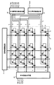
FIG. 1 is a configuration diagram of a liquid crystal display device according to a first embodiment.
FIG. 2 is a detailed configuration diagram around one pixel electrode of the liquid crystal display device according to the first embodiment;
3 is an operation timing chart of the liquid crystal display device of
4 is a configuration diagram of a liquid crystal display device of
FIG. 5 is an operation timing chart of the liquid crystal display device according to the second embodiment.
6 is a configuration diagram of a liquid crystal display device of
7 is a configuration diagram of a liquid crystal display device of Embodiment 4. FIG.
8 is a configuration diagram of a liquid crystal display device of
9 is a graph showing a luminance change rate of the liquid crystal element of
FIG. 10 is a configuration diagram of a liquid crystal display device according to a sixth embodiment.
FIG. 11 is a configuration diagram of a modulation signal amplitude adjustment circuit according to a sixth embodiment.
12 is an operation timing chart of the liquid crystal display device of
13 is a configuration diagram of a liquid crystal display device of
14 is a graph showing a luminance change rate of the liquid crystal element of
15 is an operation timing chart of the liquid crystal display device of
FIG. 16 is an operation timing chart of the liquid crystal display device according to the eighth embodiment;
FIG. 17 is a configuration diagram of a conventional liquid crystal display device.
FIG. 18 is an operation timing chart of a conventional liquid crystal display device.
[Explanation of symbols]
1 signal line
2 scanning lines
3 Switching elements
4 Pixel electrode
5 Common electrode wire
6 Retention capacity
7 Liquid crystal layer
8 Gate-drain capacitance
9 Signal line drive circuit
10 Scanning line drive circuit
11 Counter electrode
12 Common electrode line drive circuit
13 Counter electrode drive circuit
14 Reference voltage generator
15 Modulation signal amplitude adjustment circuit
20 display area
30 Source-drain capacitance
31 Gate-source capacitance
Claims (58)
前記第一の基板と対向して配された第二の基板と、
前記第一および第二の基板の間に挟持された液晶層と、
前記画素電極との間に前記液晶層を駆動するための電界を形成するために前記第一または第二の基板に配された対向電極と、
前記信号線およびスイッチング素子を介して前記画素電極に画像信号を出力する信号線駆動回路と、
前記走査線を介して前記スイッチング素子に前記走査信号を出力する走査線駆動回路と、
前記画像信号の論理極性に対応して前記共通電極線に2レベルの変調信号を出力し、前記変調信号は前記走査線がスイッチング素子をオフした後、1乃至Nライン後に変調セットタイミングを有し、前記走査線がスイッチング素子をオフする前1乃至Mライン以前にレベル変更のためのリセットタイミングを有し、N+Mは全ライン数の10%以下で、前記リセットタイミングから前記変調セットタイミングまでの時間は前記走査線が前記スイッチング素子をオンしている期間を含み、前記変調信号の振幅は2レベルのうちの絶対値の大きい方であり3値の電圧からなる共通電極線駆動回路とを具備する液晶表示装置。A plurality of signal lines arranged in parallel to each other, a plurality of scanning lines orthogonal to the signal lines, pixel electrodes formed in the signal lines and regions surrounded by the scanning lines, and scanning signals input from the scanning lines And a plurality of switching elements that control connection between each of the pixel electrodes and the signal line, and are arranged in parallel with the scanning line in a pair with the scanning line and held between the pixel electrode A first substrate with a common electrode forming a capacitor;
A second substrate disposed opposite the first substrate;
A liquid crystal layer sandwiched between the first and second substrates;
A counter electrode disposed on the first or second substrate to form an electric field for driving the liquid crystal layer between the pixel electrode and the pixel electrode;
A signal line driving circuit that outputs an image signal to the pixel electrode via the signal line and the switching element;
A scanning line driving circuit for outputting the scanning signal to the switching element via the scanning line;
A two-level modulation signal is output to the common electrode line corresponding to the logical polarity of the image signal, and the modulation signal has a modulation set timing one to N lines after the scanning line turns off the switching element. , The scan line has a reset timing for level change 1 to M lines before the switching element is turned off, and N + M is 10% or less of the total number of lines, and the time from the reset timing to the modulation set timing Includes a period during which the scanning line is turned on, and the amplitude of the modulation signal has a larger absolute value of two levels, and a common electrode line driving circuit composed of a ternary voltage. Liquid crystal display device.
前記第一の基板と対向して配された第二の基板と、
前記第一および第二の基板の間に挟持された液晶層と、
前記画素電極との間に前記液晶層を駆動するための電界を形成するために前記第一または第二の基板に配された対向電極と、
前記信号線およびスイッチング素子を介して前記画素電極に画像信号を出力する信号線駆動回路と、
前記走査線を介して前記スイッチング素子に前記走査信号を出力する走査線駆動回路と、
前記画像信号の論理極性に対応して前記共通電極線に2レベルの変調信号を出力し、前記変調信号は前記走査線がスイッチング素子をオフした後、1乃至Nライン後に変調セットタイミングを有し、前記走査線がスイッチング素子をオフする前1乃至Mライン以前にレベル変更のためのリセットタイミングを有し、N+Mは全ライン数の10%以下で、前記リセットタイミングから前記変調セットタイミングまでの時間は前記走査線が前記スイッチング素子をオンしている期間を含み、前記変調信号の振幅は2レベルのうちの絶対値の大きい方であり4値の電圧からなる共通電極線駆動回路とを具備する液晶表示装置。A plurality of signal lines arranged in parallel to each other, a plurality of scanning lines orthogonal to the signal lines, pixel electrodes formed in the signal lines and regions surrounded by the scanning lines, and scanning signals input from the scanning lines And a plurality of switching elements that control connection between each of the pixel electrodes and the signal line, and are arranged in parallel with the scanning line in a pair with the scanning line and held between the pixel electrode A first substrate with a common electrode forming a capacitor;
A second substrate disposed opposite the first substrate;
A liquid crystal layer sandwiched between the first and second substrates;
A counter electrode disposed on the first or second substrate to form an electric field for driving the liquid crystal layer between the pixel electrode and the pixel electrode;
A signal line driving circuit that outputs an image signal to the pixel electrode via the signal line and the switching element;
A scanning line driving circuit for outputting the scanning signal to the switching element via the scanning line;
A two-level modulation signal is output to the common electrode line corresponding to the logical polarity of the image signal, and the modulation signal has a modulation set timing one to N lines after the scanning line turns off the switching element. , The scan line has a reset timing for level change 1 to M lines before the switching element is turned off, and N + M is 10% or less of the total number of lines, and the time from the reset timing to the modulation set timing Includes a period during which the scanning line turns on the switching element, and the amplitude of the modulation signal is a larger one of the absolute values of the two levels, and a common electrode line driving circuit composed of a quaternary voltage. Liquid crystal display device.
前記第一の基板と対向して配された第二の基板と、
前記第一および第二の基板の間に挟持された液晶層と、
前記画素電極との間に前記液晶層を駆動するための電界を形成するために前記第一または第二の基板に配された対向電極と、
前記信号線およびスイッチング素子を介して前記画素電極に画像信号を出力する信号線駆動回路と、
前記画像信号の電位を決める電位発生回路と、
前記走査線を介して前記スイッチング素子に前記走査信号を出力する走査線駆動回路と、
前記画像信号の論理極性に対応して前記共通電極線に2レベルの変調信号を出力し、前記変調信号は前記走査線がスイッチング素子をオフした後、1乃至Nライン後に変調セットタイミングを有し、前記走査線がスイッチング素子をオフする前1乃至Mライン以前にレベル変更のためのリセットタイミングを有し、N+Mは全ライン数の10%以下で、前記リセットタイミングから前記変調セットタイミングまでの時間は前記走査線が前記スイッチング素子をオンしている期間を含み、前記変調信号の振幅は2レベルのうちの絶対値の大きい方である共通電極線駆動回路とを具備し、前記共通線駆動回路が使用する電圧の一部と前記電位発生回路が使用する電圧の一部とを共用する液晶表示装置。A plurality of signal lines arranged in parallel to each other, a plurality of scanning lines orthogonal to the signal lines, pixel electrodes formed in the signal lines and regions surrounded by the scanning lines, and scanning signals input from the scanning lines And a plurality of switching elements that control connection between each of the pixel electrodes and the signal line, and are arranged in parallel with the scanning line in a pair with the scanning line and held between the pixel electrode A first substrate with a common electrode forming a capacitor;
A second substrate disposed opposite the first substrate;
A liquid crystal layer sandwiched between the first and second substrates;
A counter electrode disposed on the first or second substrate to form an electric field for driving the liquid crystal layer between the pixel electrode and the pixel electrode;
A signal line driving circuit that outputs an image signal to the pixel electrode via the signal line and the switching element;
A potential generation circuit for determining the potential of the image signal;
A scanning line driving circuit for outputting the scanning signal to the switching element via the scanning line;
A two-level modulation signal is output to the common electrode line corresponding to the logical polarity of the image signal, and the modulation signal has a modulation set timing one to N lines after the scanning line turns off the switching element. , The scan line has a reset timing for level change 1 to M lines before the switching element is turned off, and N + M is 10% or less of the total number of lines, and the time from the reset timing to the modulation set timing Includes a common electrode line driving circuit including a period during which the scanning line is turning on the switching element, and the amplitude of the modulation signal having a larger absolute value of two levels, and the common line driving circuit A liquid crystal display device that shares a part of the voltage used by and a part of the voltage used by the potential generating circuit.
前記第一の基板と対向して配された第二の基板と、
前記第一および第二の基板の間に挟持された液晶層と、
前記画素電極との間に前記液晶層を駆動するための電界を形成するために前記第一または第二の基板に配された対向電極と、
前記信号線およびスイッチング素子を介して前記画素電極に画像信号を出力する信号線駆動回路と、
前記走査線を介して前記スイッチング素子に前記走査信号を出力する走査線駆動回路と、
前記画像信号の論理極性に対応して前記共通電極線に2レベルの変調信号を出力し、前記変調信号は前記走査線がスイッチング素子をオフした後、1乃至Nライン後に変調セットタイミングを有し、前記走査線がスイッチング素子をオフする前1乃至Mライン以前にレベル変更のためのリセットタイミングを有し、N+Mは全ライン数の10%以下で、前記リセットタイミングから前記変調セットタイミングまでの時間は前記走査線が前記スイッチング素子をオンしている期間を含み、前記変調信号の振幅は2レベルのうちの絶対値の大きい方である共通電極線駆動回路とを具備し、前記共通線駆動回路が使用する電圧の一部と前記対向電極電位とを共用する液晶表示装置。A plurality of signal lines arranged in parallel to each other, a plurality of scanning lines orthogonal to the signal lines, pixel electrodes formed in the signal lines and regions surrounded by the scanning lines, and scanning signals input from the scanning lines And a plurality of switching elements that control connection between each of the pixel electrodes and the signal line, and are arranged in parallel with the scanning line in a pair with the scanning line and held between the pixel electrode A first substrate with a common electrode forming a capacitor;
A second substrate disposed opposite the first substrate;
A liquid crystal layer sandwiched between the first and second substrates;
A counter electrode disposed on the first or second substrate to form an electric field for driving the liquid crystal layer between the pixel electrode and the pixel electrode;
A signal line driving circuit that outputs an image signal to the pixel electrode via the signal line and the switching element;
A scanning line driving circuit for outputting the scanning signal to the switching element via the scanning line;
A two-level modulation signal is output to the common electrode line corresponding to the logical polarity of the image signal, and the modulation signal has a modulation set timing one to N lines after the scanning line turns off the switching element. , The scan line has a reset timing for level change 1 to M lines before the switching element is turned off, and N + M is 10% or less of the total number of lines, and the time from the reset timing to the modulation set timing Includes a common electrode line driving circuit including a period during which the scanning line is turning on the switching element, and the amplitude of the modulation signal having a larger absolute value of two levels, and the common line driving circuit A liquid crystal display device which shares a part of the voltage used by and the counter electrode potential.
前記第一の基板と対向して配された第二の基板と、
前記第一および第二の基板の間に挟持された液晶層と、
前記画素電極との間に前記液晶層を駆動するための電界を形成するために前記第一または第二の基板に配された対向電極と、
前記信号線およびスイッチング素子を介して前記画素電極に画像信号を出力する信号線駆動回路と、
前記走査線を介して前記スイッチング素子に前記走査信号を出力する走査線駆動回路と、
前記画像信号の論理極性に対応して前記共通電極線に2レベルの変調信号を出力し、前記変調信号は前記走査線がスイッチング素子をオフした後、1乃至Nライン後に変調セットタイミングを有し、前記走査線がスイッチング素子をオフする前1乃至Mライン以前にレベル変更のためのリセットタイミングを有し、N+Mは全ライン数の10%以下で、前記リセットタイミングから前記変調セットタイミングまでの時間は前記走査線が前記スイッチング素子をオンしている期間を含み、前記変調信号の振幅は2レベルのうちの絶対値の大きい方で、液晶表示装置としての輝度を変更するための変調信号振幅調整機能を有する共通電極線駆動回路とを具備する液晶表示装置。A plurality of signal lines arranged in parallel to each other, a plurality of scanning lines orthogonal to the signal lines, pixel electrodes formed in the signal lines and regions surrounded by the scanning lines, and scanning signals input from the scanning lines And a plurality of switching elements that control connection between each of the pixel electrodes and the signal line, and are arranged in parallel with the scanning line in a pair with the scanning line and held between the pixel electrode A first substrate with a common electrode forming a capacitor;
A second substrate disposed opposite the first substrate;
A liquid crystal layer sandwiched between the first and second substrates;
A counter electrode disposed on the first or second substrate to form an electric field for driving the liquid crystal layer between the pixel electrode and the pixel electrode;
A signal line driving circuit that outputs an image signal to the pixel electrode via the signal line and the switching element;
A scanning line driving circuit for outputting the scanning signal to the switching element via the scanning line;
A two-level modulation signal is output to the common electrode line corresponding to the logical polarity of the image signal, and the modulation signal has a modulation set timing one to N lines after the scanning line turns off the switching element. , The scan line has a reset timing for level change 1 to M lines before the switching element is turned off, and N + M is 10% or less of the total number of lines, and the time from the reset timing to the modulation set timing Includes a period during which the scanning line is ON, and the amplitude of the modulation signal is the larger one of the absolute values of the two levels, and the modulation signal amplitude adjustment for changing the luminance of the liquid crystal display device A liquid crystal display device comprising a common electrode line driving circuit having a function.
前記第一の基板と対向して配された第二の基板と、
前記第一および第二の基板の間に挟持された液晶層と、
前記画素電極との間に前記液晶層を駆動するための電界を形成するために前記第一または第二の基板に配された対向電極と、
前記信号線およびスイッチング素子を介して前記画素電極に画像信号を出力する信号線駆動回路と、
前記走査線を介して前記スイッチング素子に前記走査信号を出力する走査線駆動回路と、
前記画像信号の論理極性に対応して前記共通電極線に2レベルの変調信号を出力し、前記変調信号は前記走査線がスイッチング素子をオフした後、1乃至Nライン後に変調セットタイミングを有し、前記走査線がスイッチング素子をオフする前1乃至Mライン以前にレベル変更のためのリセットタイミングを有し、N+Mは全ライン数の10%以下で、前記リセットタイミングから前記変調セットタイミングまでの時間は前記走査線が前記スイッチング素子をオンしている期間を含み、前記変調信号の振幅は2レベルのうちの絶対値の大きい方で、液晶表示装置としての輝度を変更するための変調信号振幅調整機能を有する共通電極線駆動回路と、
前記変調信号振幅調整機能に対応して対向電極電位が変化する対向電位変動調整装置とを具備する液晶表示装置。A plurality of signal lines arranged in parallel to each other, a plurality of scanning lines orthogonal to the signal lines, pixel electrodes formed in the signal lines and regions surrounded by the scanning lines, and scanning signals input from the scanning lines And a plurality of switching elements that control connection between each of the pixel electrodes and the signal line, and are arranged in parallel with the scanning line in a pair with the scanning line and held between the pixel electrode A first substrate with a common electrode forming a capacitor;
A second substrate disposed opposite the first substrate;
A liquid crystal layer sandwiched between the first and second substrates;
A counter electrode disposed on the first or second substrate to form an electric field for driving the liquid crystal layer between the pixel electrode and the pixel electrode;
A signal line driving circuit that outputs an image signal to the pixel electrode via the signal line and the switching element;
A scanning line driving circuit for outputting the scanning signal to the switching element via the scanning line;
A two-level modulation signal is output to the common electrode line corresponding to the logical polarity of the image signal, and the modulation signal has a modulation set timing one to N lines after the scanning line turns off the switching element. , The scan line has a reset timing for level change 1 to M lines before the switching element is turned off, and N + M is 10% or less of the total number of lines, and the time from the reset timing to the modulation set timing Includes a period during which the scanning line is ON, and the amplitude of the modulation signal is the larger one of the absolute values of the two levels, and the modulation signal amplitude adjustment for changing the luminance of the liquid crystal display device A common electrode line driving circuit having a function ;
A liquid crystal display device comprising: a counter potential fluctuation adjusting device that changes a counter electrode potential corresponding to the modulation signal amplitude adjusting function.
前記第一の基板と対向して配された第二の基板と、
前記第一および第二の基板の間に挟持された液晶層と、
前記画素電極との間に前記液晶層を駆動するための電界を形成するために前記第一または第二の基板に配された対向電極と、
前記信号線およびスイッチング素子を介して前記画素電極に画像信号を出力する信号線駆動回路と、
前記画像信号振幅を調整する画像信号振幅調整回路と前記走査線を介して前記スイッチング素子に前記走査信号を出力する走査線駆動回路と、
前記画像信号の論理極性に対応して前記共通電極線に2レベルの変調信号を出力し、前記変調信号は前記走査線がスイッチング素子をオフした後、1乃至Nライン後に変調セットタイミングを有し、前記走査線がスイッチング素子をオフする前1乃至Mライン以前にレベル変更のためのリセットタイミングを有し、N+Mは全ライン数の10%以下で、前記リセットタイミングから前記変調セットタイミングまでの時間は前記走査線が前記スイッチング素子をオンしている期間を含み、前記変調信号の振幅は2レベルのうちの絶対値の大きい方で、液晶表示装置としての輝度を変更するための変調信号振幅調整機能を有する共通電極線駆動回路とを具備する液晶表示装置。A plurality of signal lines arranged in parallel to each other, a plurality of scanning lines orthogonal to the signal lines, pixel electrodes formed in the signal lines and regions surrounded by the scanning lines, and scanning signals input from the scanning lines And a plurality of switching elements that control connection between each of the pixel electrodes and the signal line, and are arranged in parallel with the scanning line in a pair with the scanning line and held between the pixel electrode A first substrate with a common electrode forming a capacitor;
A second substrate disposed opposite the first substrate;
A liquid crystal layer sandwiched between the first and second substrates;
A counter electrode disposed on the first or second substrate to form an electric field for driving the liquid crystal layer between the pixel electrode and the pixel electrode;
A signal line driving circuit that outputs an image signal to the pixel electrode via the signal line and the switching element;
An image signal amplitude adjusting circuit for adjusting the image signal amplitude, and a scanning line driving circuit for outputting the scanning signal to the switching element via the scanning line;
A two-level modulation signal is output to the common electrode line corresponding to the logical polarity of the image signal, and the modulation signal has a modulation set timing one to N lines after the scanning line turns off the switching element. , The scan line has a reset timing for level change 1 to M lines before the switching element is turned off, and N + M is 10% or less of the total number of lines, and the time from the reset timing to the modulation set timing Includes a period during which the scanning line is ON, and the amplitude of the modulation signal is the larger one of the absolute values of the two levels, and the modulation signal amplitude adjustment for changing the luminance of the liquid crystal display device A liquid crystal display device comprising a common electrode line driving circuit having a function.
前記第一の基板と対向して配された第二の基板と、
前記第一および第二の基板の間に挟持された液晶層と、
前記画素電極との間に前記液晶層を駆動するための電界を形成するために前記第一または第二の基板に配された対向電極と、
前記信号線およびスイッチング素子を介して前記画素電極に画像信号を出力する信号線駆動回路と、
前記走査線を介して前記スイッチング素子に前記走査信号を出力する走査線駆動回路と、
前記画像信号の論理極性に対応して前記共通電極線に2レベルの変調信号を出力し、前記変調信号は前記走査線がスイッチング素子をオフした後、1乃至Nライン後に変調セットタイミングを有し、前記走査線がスイッチング素子をオフする前1乃至Mライン以前にレベル変更のためのリセットタイミングを有し、N+Mは全ライン数の10%以下で、前記リセットタイミングから前記変調セットタイミングまでの時間は前記走査線が前記スイッチング素子をオンしている期間を含み、走査線のオンオフタイミングに対する前記変調タイミング、リセットタイミングの時間的相関関係を走査線ごとに任意に設定でき、前記変調信号の振幅は2レベルのうちの絶対値の大きい方である共通電極線駆動回路とを具備する液晶表示装置。A plurality of signal lines arranged in parallel to each other, a plurality of scanning lines orthogonal to the signal lines, pixel electrodes formed in the signal lines and regions surrounded by the scanning lines, and scanning signals input from the scanning lines And a plurality of switching elements that control connection between each of the pixel electrodes and the signal line, and are arranged in parallel with the scanning line in a pair with the scanning line and held between the pixel electrode A first substrate with a common electrode forming a capacitor;
A second substrate disposed opposite the first substrate;
A liquid crystal layer sandwiched between the first and second substrates;
A counter electrode disposed on the first or second substrate to form an electric field for driving the liquid crystal layer between the pixel electrode and the pixel electrode;
A signal line driving circuit that outputs an image signal to the pixel electrode via the signal line and the switching element;
A scanning line driving circuit for outputting the scanning signal to the switching element via the scanning line;
A two-level modulation signal is output to the common electrode line corresponding to the logical polarity of the image signal, and the modulation signal has a modulation set timing one to N lines after the scanning line turns off the switching element. , The scan line has a reset timing for level change 1 to M lines before the switching element is turned off, and N + M is 10% or less of the total number of lines, and the time from the reset timing to the modulation set timing Includes a period in which the scanning line is on, and the temporal correlation of the modulation timing and reset timing with respect to the on / off timing of the scanning line can be arbitrarily set for each scanning line, and the amplitude of the modulation signal is A liquid crystal display device comprising a common electrode line driving circuit having a larger absolute value of two levels.
Priority Applications (1)
| Application Number | Priority Date | Filing Date | Title |
|---|---|---|---|
| JP2001189233A JP4801848B2 (en) | 2001-06-22 | 2001-06-22 | Liquid crystal display |
Applications Claiming Priority (1)
| Application Number | Priority Date | Filing Date | Title |
|---|---|---|---|
| JP2001189233A JP4801848B2 (en) | 2001-06-22 | 2001-06-22 | Liquid crystal display |
Publications (2)
| Publication Number | Publication Date |
|---|---|
| JP2003005721A JP2003005721A (en) | 2003-01-08 |
| JP4801848B2 true JP4801848B2 (en) | 2011-10-26 |
Family
ID=19028188
Family Applications (1)
| Application Number | Title | Priority Date | Filing Date |
|---|---|---|---|
| JP2001189233A Expired - Fee Related JP4801848B2 (en) | 2001-06-22 | 2001-06-22 | Liquid crystal display |
Country Status (1)
| Country | Link |
|---|---|
| JP (1) | JP4801848B2 (en) |
Families Citing this family (5)
| Publication number | Priority date | Publication date | Assignee | Title |
|---|---|---|---|---|
| JP4275588B2 (en) | 2004-07-26 | 2009-06-10 | シャープ株式会社 | Liquid crystal display |
| KR101352343B1 (en) * | 2006-12-11 | 2014-01-15 | 삼성디스플레이 주식회사 | Liquid Crystal Display |
| KR101540072B1 (en) | 2007-10-16 | 2015-07-28 | 삼성디스플레이 주식회사 | Liquid crystal display apparatus |
| WO2009137241A2 (en) | 2008-04-14 | 2009-11-12 | Bandgap Engineering, Inc. | Process for fabricating nanowire arrays |
| JP2011191773A (en) * | 2011-04-28 | 2011-09-29 | Sanyo Electric Co Ltd | Display device |
Family Cites Families (4)
| Publication number | Priority date | Publication date | Assignee | Title |
|---|---|---|---|---|
| JPH0572999A (en) * | 1991-09-17 | 1993-03-26 | Hitachi Ltd | Liquid crystal display device and its driving method |
| JP2806098B2 (en) * | 1991-10-09 | 1998-09-30 | 松下電器産業株式会社 | Driving method of display device |
| JP3483759B2 (en) * | 1998-03-19 | 2004-01-06 | 株式会社東芝 | Liquid crystal display |
| JP3886698B2 (en) * | 1999-03-31 | 2007-02-28 | 株式会社半導体エネルギー研究所 | Liquid crystal display device, driving method of liquid crystal display device, display, projector, goggle type display, portable information terminal, and computer |
-
2001
- 2001-06-22 JP JP2001189233A patent/JP4801848B2/en not_active Expired - Fee Related
Also Published As
| Publication number | Publication date |
|---|---|
| JP2003005721A (en) | 2003-01-08 |
Similar Documents
| Publication | Publication Date | Title |
|---|---|---|
| US7973757B2 (en) | Liquid crystal display | |
| US8098219B2 (en) | Liquid crystal display panel, liquid crystal display device having the same, and driving method thereof | |
| US8149232B2 (en) | Systems and methods for generating reference voltages | |
| US20050253829A1 (en) | Display device and display device driving method | |
| US7999803B2 (en) | Liquid crystal display device having drive circuit | |
| JP3240367B2 (en) | Active matrix type liquid crystal image display | |
| US7321352B2 (en) | Liquid crystal display and method for driving the same | |
| US8232932B2 (en) | Display device | |
| JP3906665B2 (en) | Liquid crystal drive device | |
| EP2219175B1 (en) | Driving circuit and voltage generating circuit and display using the same | |
| CN101320552A (en) | Half data driving pixel driving method of liquid crystal display device | |
| JPH07181927A (en) | Image display device | |
| JP4204204B2 (en) | Active matrix display device | |
| JP2001133808A (en) | Liquid crystal display device and driving method thereof | |
| CN102763031B (en) | Liquid-crystal display device | |
| JP4801848B2 (en) | Liquid crystal display | |
| KR100701137B1 (en) | Active matrix display | |
| JP2005128101A (en) | Liquid crystal display device | |
| JP5418388B2 (en) | Liquid crystal display | |
| US8878832B2 (en) | Pixel circuit, display device, and method for driving display device | |
| JP4278314B2 (en) | Active matrix display device | |
| US9626920B2 (en) | Liquid crystal display device and method for driving same | |
| JP4907035B2 (en) | Liquid crystal display device and driving method thereof | |
| JP4197852B2 (en) | Active matrix display device | |
| JP4297629B2 (en) | Active matrix display device |
Legal Events
| Date | Code | Title | Description |
|---|---|---|---|
| A711 | Notification of change in applicant |
Free format text: JAPANESE INTERMEDIATE CODE: A711 Effective date: 20061109 |
|
| A621 | Written request for application examination |
Free format text: JAPANESE INTERMEDIATE CODE: A621 Effective date: 20080520 |
|
| A131 | Notification of reasons for refusal |
Free format text: JAPANESE INTERMEDIATE CODE: A131 Effective date: 20110426 |
|
| A521 | Written amendment |
Free format text: JAPANESE INTERMEDIATE CODE: A523 Effective date: 20110622 |
|
| TRDD | Decision of grant or rejection written | ||
| A01 | Written decision to grant a patent or to grant a registration (utility model) |
Free format text: JAPANESE INTERMEDIATE CODE: A01 Effective date: 20110712 |
|
| A01 | Written decision to grant a patent or to grant a registration (utility model) |
Free format text: JAPANESE INTERMEDIATE CODE: A01 |
|
| A61 | First payment of annual fees (during grant procedure) |
Free format text: JAPANESE INTERMEDIATE CODE: A61 Effective date: 20110808 |
|
| FPAY | Renewal fee payment (event date is renewal date of database) |
Free format text: PAYMENT UNTIL: 20140812 Year of fee payment: 3 |
|
| R150 | Certificate of patent or registration of utility model |
Ref document number: 4801848 Country of ref document: JP Free format text: JAPANESE INTERMEDIATE CODE: R150 Free format text: JAPANESE INTERMEDIATE CODE: R150 |
|
| S533 | Written request for registration of change of name |
Free format text: JAPANESE INTERMEDIATE CODE: R313533 |
|
| FPAY | Renewal fee payment (event date is renewal date of database) |
Free format text: PAYMENT UNTIL: 20140812 Year of fee payment: 3 |
|
| R350 | Written notification of registration of transfer |
Free format text: JAPANESE INTERMEDIATE CODE: R350 |
|
| R250 | Receipt of annual fees |
Free format text: JAPANESE INTERMEDIATE CODE: R250 |
|
| R250 | Receipt of annual fees |
Free format text: JAPANESE INTERMEDIATE CODE: R250 |
|
| R250 | Receipt of annual fees |
Free format text: JAPANESE INTERMEDIATE CODE: R250 |
|
| R250 | Receipt of annual fees |
Free format text: JAPANESE INTERMEDIATE CODE: R250 |
|
| R250 | Receipt of annual fees |
Free format text: JAPANESE INTERMEDIATE CODE: R250 |
|
| LAPS | Cancellation because of no payment of annual fees |