JP4814200B2 - 高分解能露光ツールの像コントラストの強化 - Google Patents
高分解能露光ツールの像コントラストの強化 Download PDFInfo
- Publication number
- JP4814200B2 JP4814200B2 JP2007296176A JP2007296176A JP4814200B2 JP 4814200 B2 JP4814200 B2 JP 4814200B2 JP 2007296176 A JP2007296176 A JP 2007296176A JP 2007296176 A JP2007296176 A JP 2007296176A JP 4814200 B2 JP4814200 B2 JP 4814200B2
- Authority
- JP
- Japan
- Prior art keywords
- substrate
- diffraction order
- patterned beam
- patterning device
- radiation
- Prior art date
- Legal status (The legal status is an assumption and is not a legal conclusion. Google has not performed a legal analysis and makes no representation as to the accuracy of the status listed.)
- Expired - Fee Related
Links
- 239000000758 substrate Substances 0.000 claims description 157
- 230000005855 radiation Effects 0.000 claims description 127
- 238000000059 patterning Methods 0.000 claims description 89
- 230000003287 optical effect Effects 0.000 claims description 47
- 238000005286 illumination Methods 0.000 claims description 43
- 210000001747 pupil Anatomy 0.000 claims description 23
- 238000000034 method Methods 0.000 claims description 20
- 230000002238 attenuated effect Effects 0.000 claims description 17
- 230000010363 phase shift Effects 0.000 claims description 16
- 239000000463 material Substances 0.000 claims description 8
- 230000008859 change Effects 0.000 claims description 7
- 238000001459 lithography Methods 0.000 claims description 7
- 230000002093 peripheral effect Effects 0.000 claims description 3
- 239000010453 quartz Substances 0.000 claims description 2
- VYPSYNLAJGMNEJ-UHFFFAOYSA-N silicon dioxide Inorganic materials O=[Si]=O VYPSYNLAJGMNEJ-UHFFFAOYSA-N 0.000 claims description 2
- 239000010410 layer Substances 0.000 description 14
- 208000006011 Stroke Diseases 0.000 description 10
- 238000003491 array Methods 0.000 description 9
- 238000009826 distribution Methods 0.000 description 9
- 238000004519 manufacturing process Methods 0.000 description 8
- 230000003068 static effect Effects 0.000 description 8
- 238000010586 diagram Methods 0.000 description 5
- 238000007654 immersion Methods 0.000 description 5
- 239000007788 liquid Substances 0.000 description 5
- PXHVJJICTQNCMI-UHFFFAOYSA-N Nickel Chemical compound [Ni] PXHVJJICTQNCMI-UHFFFAOYSA-N 0.000 description 4
- 238000006243 chemical reaction Methods 0.000 description 4
- QSHDDOUJBYECFT-UHFFFAOYSA-N mercury Chemical compound [Hg] QSHDDOUJBYECFT-UHFFFAOYSA-N 0.000 description 4
- 229910052753 mercury Inorganic materials 0.000 description 4
- 230000008569 process Effects 0.000 description 4
- 238000012545 processing Methods 0.000 description 4
- 230000002745 absorbent Effects 0.000 description 3
- 239000002250 absorbent Substances 0.000 description 3
- 238000013461 design Methods 0.000 description 3
- 238000005530 etching Methods 0.000 description 3
- 238000003384 imaging method Methods 0.000 description 3
- 239000011159 matrix material Substances 0.000 description 3
- 230000009467 reduction Effects 0.000 description 3
- 239000010409 thin film Substances 0.000 description 3
- VYZAMTAEIAYCRO-UHFFFAOYSA-N Chromium Chemical compound [Cr] VYZAMTAEIAYCRO-UHFFFAOYSA-N 0.000 description 2
- 229910052804 chromium Inorganic materials 0.000 description 2
- 239000011651 chromium Substances 0.000 description 2
- 230000007423 decrease Effects 0.000 description 2
- 230000000694 effects Effects 0.000 description 2
- 239000011521 glass Substances 0.000 description 2
- 239000002346 layers by function Substances 0.000 description 2
- 229910052759 nickel Inorganic materials 0.000 description 2
- 238000000206 photolithography Methods 0.000 description 2
- 230000002829 reductive effect Effects 0.000 description 2
- 230000004044 response Effects 0.000 description 2
- 239000004065 semiconductor Substances 0.000 description 2
- 229910052710 silicon Inorganic materials 0.000 description 2
- 238000012876 topography Methods 0.000 description 2
- 230000007704 transition Effects 0.000 description 2
- 229910001218 Gallium arsenide Inorganic materials 0.000 description 1
- 229910000673 Indium arsenide Inorganic materials 0.000 description 1
- 229910003811 SiGeC Inorganic materials 0.000 description 1
- XUIMIQQOPSSXEZ-UHFFFAOYSA-N Silicon Chemical compound [Si] XUIMIQQOPSSXEZ-UHFFFAOYSA-N 0.000 description 1
- 229910000577 Silicon-germanium Inorganic materials 0.000 description 1
- 239000011358 absorbing material Substances 0.000 description 1
- 239000000919 ceramic Substances 0.000 description 1
- 150000001875 compounds Chemical class 0.000 description 1
- 230000001010 compromised effect Effects 0.000 description 1
- 238000001514 detection method Methods 0.000 description 1
- 238000011161 development Methods 0.000 description 1
- 230000009977 dual effect Effects 0.000 description 1
- 230000005684 electric field Effects 0.000 description 1
- 230000005670 electromagnetic radiation Effects 0.000 description 1
- 230000006870 function Effects 0.000 description 1
- RPQDHPTXJYYUPQ-UHFFFAOYSA-N indium arsenide Chemical compound [In]#[As] RPQDHPTXJYYUPQ-UHFFFAOYSA-N 0.000 description 1
- 238000007689 inspection Methods 0.000 description 1
- 230000003993 interaction Effects 0.000 description 1
- 230000002452 interceptive effect Effects 0.000 description 1
- 239000004973 liquid crystal related substance Substances 0.000 description 1
- 230000005381 magnetic domain Effects 0.000 description 1
- 238000012986 modification Methods 0.000 description 1
- 230000004048 modification Effects 0.000 description 1
- 229910003465 moissanite Inorganic materials 0.000 description 1
- 230000036961 partial effect Effects 0.000 description 1
- 238000002360 preparation method Methods 0.000 description 1
- 238000007493 shaping process Methods 0.000 description 1
- 239000010703 silicon Substances 0.000 description 1
- 229910010271 silicon carbide Inorganic materials 0.000 description 1
- 239000007787 solid Substances 0.000 description 1
- 230000001360 synchronised effect Effects 0.000 description 1
- XLYOFNOQVPJJNP-UHFFFAOYSA-N water Substances O XLYOFNOQVPJJNP-UHFFFAOYSA-N 0.000 description 1
- 238000003079 width control Methods 0.000 description 1
Images

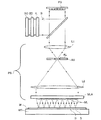


Classifications
-
- G—PHYSICS
- G03—PHOTOGRAPHY; CINEMATOGRAPHY; ANALOGOUS TECHNIQUES USING WAVES OTHER THAN OPTICAL WAVES; ELECTROGRAPHY; HOLOGRAPHY
- G03F—PHOTOMECHANICAL PRODUCTION OF TEXTURED OR PATTERNED SURFACES, e.g. FOR PRINTING, FOR PROCESSING OF SEMICONDUCTOR DEVICES; MATERIALS THEREFOR; ORIGINALS THEREFOR; APPARATUS SPECIALLY ADAPTED THEREFOR
- G03F7/00—Photomechanical, e.g. photolithographic, production of textured or patterned surfaces, e.g. printing surfaces; Materials therefor, e.g. comprising photoresists; Apparatus specially adapted therefor
- G03F7/70—Microphotolithographic exposure; Apparatus therefor
- G03F7/70058—Mask illumination systems
- G03F7/70191—Optical correction elements, filters or phase plates for controlling intensity, wavelength, polarisation, phase or the like
-
- G—PHYSICS
- G03—PHOTOGRAPHY; CINEMATOGRAPHY; ANALOGOUS TECHNIQUES USING WAVES OTHER THAN OPTICAL WAVES; ELECTROGRAPHY; HOLOGRAPHY
- G03F—PHOTOMECHANICAL PRODUCTION OF TEXTURED OR PATTERNED SURFACES, e.g. FOR PRINTING, FOR PROCESSING OF SEMICONDUCTOR DEVICES; MATERIALS THEREFOR; ORIGINALS THEREFOR; APPARATUS SPECIALLY ADAPTED THEREFOR
- G03F7/00—Photomechanical, e.g. photolithographic, production of textured or patterned surfaces, e.g. printing surfaces; Materials therefor, e.g. comprising photoresists; Apparatus specially adapted therefor
- G03F7/70—Microphotolithographic exposure; Apparatus therefor
- G03F7/70058—Mask illumination systems
- G03F7/70091—Illumination settings, i.e. intensity distribution in the pupil plane or angular distribution in the field plane; On-axis or off-axis settings, e.g. annular, dipole or quadrupole settings; Partial coherence control, i.e. sigma or numerical aperture [NA]
Landscapes
- Physics & Mathematics (AREA)
- General Physics & Mathematics (AREA)
- Exposure And Positioning Against Photoresist Photosensitive Materials (AREA)
- Exposure Of Semiconductors, Excluding Electron Or Ion Beam Exposure (AREA)
Description
Claims (9)
- (a)非環状照明モードを有する放射ビームの少なくともオフアクシス部分を用いて位相シフトパターニングデバイスを照明することと、
(b)投影システムの瞳の環状周縁端部において前記パターニングされたビームの一次回折次数部分を減衰させて、前記パターニングされたビームのゼロ回折次数部分および前記一次回折次数部分の強度を前記減衰を介して実質的に均等化することと、
(c)前記パターニングされたビームの前記減衰された一次回折次数部分および前記ゼロ回折次数部分を前記投影システムを用いて基板のターゲット部分上に投影することと、
(d)前記パターニングされたビームの回折次数部分各々のエネルギーを検出することと、
(e)前記検出されたエネルギーに基づいて制御信号を生成することと、
を含む露光方法であって、
ステップ(b)が、リング状アテニュエータを用いて前記減衰を実行して、前記パターニングされたビームにおいて位相変化を生成させることを含み、
ステップ(c)の前に、ステップ(b)で生成された前記位相変化を補償することを更に含み、
前記アテニュエータが、前記制御信号に対応する個々の領域で透過ビームの減衰量が変化するように構成された可変アテニュエータであり、少なくとも前記パターニングされたビームのゼロ回折次数部分を減衰させる第1の減衰リング、および前記パターニングされたビームの一次回折次数部分を減衰させる第2の減衰リングを備える、
露光方法。 - 前記位相シフトパターニングデバイスが減衰位相シフトパターニングデバイスである、請求項1に記載の方法。
- ステップ(b)が、前記投影システムの瞳内に位置決めされた光学エレメント上に前記第1及び第2の減衰リングを形成することを更に含む、請求項1又は2に記載の方法。
- ステップ(b)が、前記光学エレメントとしてレンズを用いることを更に含む、請求項3に記載の方法。
- ステップ(b)において、前記光学エレメントが石英材料を含む、請求項3又は4に記載の方法。
- 前記投影システムの前記瞳を出入りするように配置された物体上に前記第1及び第2の減衰リングを形成することを更に含む、請求項1又は2に記載の方法。
- 前記放射ビームの非環状照明モードが2極、4極、6極または8極である、請求項1乃至6のいずれか1項に記載の方法。
- 非環状照明モードを有する放射ビームを生成する照明システムと、
前記ビームをパターニングする位相シフトパターニングデバイスと、
前記パターニングされたビームを基板のターゲット部分上に投影する投影システムであって、該投影システムの瞳の端部に位置決めされて、前記パターニングされたビームの一次回折次数部分を減衰させるリング状アテニュエータを含み、該アテニュエータが前記パターニングされたビームの一次回折次数部分の強度が前記パターニングされたビームのゼロ回折次数部分の強度と実質的に等しくされるように構成された投影システムと、
前記パターニングされたビームの回折次数部分各々のエネルギーを検出するディテクタと、
前記検出されたエネルギーに基づいて制御信号を生成するコントローラと、
を備えるリソグラフィシステムであって、
前記アテニュエータが、前記制御信号に対応する個々の領域で透過ビームの減衰量が変化するように構成された可変アテニュエータであり、少なくとも前記パターニングされたビームのゼロ回折次数部分を減衰させる第1の減衰リング、および前記パターニングされたビームの一次回折次数部分を減衰させる第2の減衰リングを備え、前記パターニングされたビームがそこを通過するときに前記パターニングされたビームにおいて位相変化を生じさせるように構成されており、
前記投影システムが、前記アテニュエータによって生成された前記パターニングされたビームにおける位相変化を補償する位相変化補償システムを更に備える、
リソグラフィシステム。 - 前記位相シフトパターニングデバイスが減衰位相シフトパターニングデバイスである、請求項8に記載のリソグラフィシステム。
Applications Claiming Priority (2)
| Application Number | Priority Date | Filing Date | Title |
|---|---|---|---|
| US11/603,243 US8054449B2 (en) | 2006-11-22 | 2006-11-22 | Enhancing the image contrast of a high resolution exposure tool |
| US11/603,243 | 2006-11-22 |
Publications (2)
| Publication Number | Publication Date |
|---|---|
| JP2008131044A JP2008131044A (ja) | 2008-06-05 |
| JP4814200B2 true JP4814200B2 (ja) | 2011-11-16 |
Family
ID=39416592
Family Applications (1)
| Application Number | Title | Priority Date | Filing Date |
|---|---|---|---|
| JP2007296176A Expired - Fee Related JP4814200B2 (ja) | 2006-11-22 | 2007-11-15 | 高分解能露光ツールの像コントラストの強化 |
Country Status (2)
| Country | Link |
|---|---|
| US (1) | US8054449B2 (ja) |
| JP (1) | JP4814200B2 (ja) |
Families Citing this family (6)
| Publication number | Priority date | Publication date | Assignee | Title |
|---|---|---|---|---|
| NL2002999A1 (nl) | 2008-06-24 | 2009-12-29 | Asml Netherlands Bv | Lithographic apparatus and device manufacturing method. |
| CN101916045B (zh) * | 2010-07-27 | 2011-11-02 | 浙江大学 | 一种用于双偶极均匀照明的自由曲面透镜 |
| CN101916046B (zh) * | 2010-07-27 | 2011-10-05 | 浙江大学 | 一种用于双环形均匀照明的自由曲面透镜 |
| CN101916047B (zh) * | 2010-07-27 | 2011-12-21 | 浙江大学 | 一种采用自由曲面透镜实现离轴照明的光刻曝光装置 |
| US20130033976A1 (en) * | 2011-08-04 | 2013-02-07 | Advanced Imaging Technologies, Inc. | Structure and method for generating an optical image from an ultrasonic holographic pattern |
| CN103106644B (zh) * | 2013-02-02 | 2016-04-27 | 南京理工大学 | 克服彩色图像非均匀光照的自适应画质增强方法 |
Family Cites Families (34)
| Publication number | Priority date | Publication date | Assignee | Title |
|---|---|---|---|---|
| US522872A (en) * | 1894-07-10 | Garden-hoe | ||
| JP3293882B2 (ja) | 1992-03-27 | 2002-06-17 | 株式会社東芝 | 投影露光装置 |
| US5523193A (en) * | 1988-05-31 | 1996-06-04 | Texas Instruments Incorporated | Method and apparatus for patterning and imaging member |
| US5296891A (en) * | 1990-05-02 | 1994-03-22 | Fraunhofer-Gesellschaft Zur Forderung Der Angewandten Forschung E.V. | Illumination device |
| EP0507487B1 (en) | 1991-04-05 | 1996-12-18 | Nippon Telegraph And Telephone Corporation | Optical projection exposure method and system using the same |
| JP2613826B2 (ja) | 1991-08-05 | 1997-05-28 | 日本電信電話株式会社 | 投影露光装置 |
| KR950004968B1 (ko) * | 1991-10-15 | 1995-05-16 | 가부시키가이샤 도시바 | 투영노광 장치 |
| US5229872A (en) | 1992-01-21 | 1993-07-20 | Hughes Aircraft Company | Exposure device including an electrically aligned electronic mask for micropatterning |
| DE69224514T2 (de) | 1992-03-23 | 1998-06-18 | Erland Torbjoern Moelnlycke Sandstroem | Verfahren und Vorrichtung zur Erzeugung eines Bildes |
| US6219015B1 (en) * | 1992-04-28 | 2001-04-17 | The Board Of Directors Of The Leland Stanford, Junior University | Method and apparatus for using an array of grating light valves to produce multicolor optical images |
| JP3224041B2 (ja) * | 1992-07-29 | 2001-10-29 | 株式会社ニコン | 露光方法及び装置 |
| JPH06181159A (ja) | 1992-12-14 | 1994-06-28 | Toshiba Corp | 投影露光装置 |
| EP0648348B1 (en) * | 1993-03-01 | 1999-04-28 | General Signal Corporation | Variable annular illuminator for photolithographic projection imager. |
| US5729331A (en) * | 1993-06-30 | 1998-03-17 | Nikon Corporation | Exposure apparatus, optical projection apparatus and a method for adjusting the optical projection apparatus |
| US6304317B1 (en) * | 1993-07-15 | 2001-10-16 | Nikon Corporation | Projection apparatus and method |
| JP3339149B2 (ja) * | 1993-12-08 | 2002-10-28 | 株式会社ニコン | 走査型露光装置ならびに露光方法 |
| JPH07301908A (ja) | 1994-05-06 | 1995-11-14 | Nippon Telegr & Teleph Corp <Ntt> | 投影露光用原図基板および投影露光方法 |
| JPH0883761A (ja) | 1994-09-09 | 1996-03-26 | Nikon Corp | 投影露光装置 |
| US5677703A (en) * | 1995-01-06 | 1997-10-14 | Texas Instruments Incorporated | Data loading circuit for digital micro-mirror device |
| US5530482A (en) * | 1995-03-21 | 1996-06-25 | Texas Instruments Incorporated | Pixel data processing for spatial light modulator having staggered pixels |
| US6133986A (en) * | 1996-02-28 | 2000-10-17 | Johnson; Kenneth C. | Microlens scanner for microlithography and wide-field confocal microscopy |
| DE69711929T2 (de) | 1997-01-29 | 2002-09-05 | Micronic Laser Systems Ab, Taeby | Verfahren und gerät zur erzeugung eines musters auf einem mit fotoresist beschichteten substrat mittels fokusiertem laserstrahl |
| US6177980B1 (en) * | 1997-02-20 | 2001-01-23 | Kenneth C. Johnson | High-throughput, maskless lithography system |
| SE509062C2 (sv) | 1997-02-28 | 1998-11-30 | Micronic Laser Systems Ab | Dataomvandlingsmetod för en laserskrivare med flera strålar för mycket komplexa mikrokolitografiska mönster |
| US5982553A (en) * | 1997-03-20 | 1999-11-09 | Silicon Light Machines | Display device incorporating one-dimensional grating light-valve array |
| SE9800665D0 (sv) * | 1998-03-02 | 1998-03-02 | Micronic Laser Systems Ab | Improved method for projection printing using a micromirror SLM |
| US6567155B1 (en) * | 2000-03-16 | 2003-05-20 | Intel Corporation | Method for improved resolution of patterning using binary masks with pupil filters |
| KR100827874B1 (ko) * | 2000-05-22 | 2008-05-07 | 가부시키가이샤 니콘 | 노광 장치, 노광 장치의 제조 방법, 노광 방법, 마이크로 장치의 제조 방법, 및 디바이스의 제조 방법 |
| JP2002324743A (ja) * | 2001-04-24 | 2002-11-08 | Canon Inc | 露光方法及び装置 |
| JP3563384B2 (ja) * | 2001-11-08 | 2004-09-08 | 大日本スクリーン製造株式会社 | 画像記録装置 |
| US6846617B2 (en) * | 2002-05-15 | 2005-01-25 | Numerical Technologies | Facilitating optical proximity effect correction through pupil filtering |
| TWI298825B (en) * | 2002-06-12 | 2008-07-11 | Asml Netherlands Bv | Lithographic apparatus and device manufacturing method |
| US6870554B2 (en) * | 2003-01-07 | 2005-03-22 | Anvik Corporation | Maskless lithography with multiplexed spatial light modulators |
| EP1482373A1 (en) * | 2003-05-30 | 2004-12-01 | ASML Netherlands B.V. | Lithographic apparatus and device manufacturing method |
-
2006
- 2006-11-22 US US11/603,243 patent/US8054449B2/en not_active Expired - Fee Related
-
2007
- 2007-11-15 JP JP2007296176A patent/JP4814200B2/ja not_active Expired - Fee Related
Also Published As
| Publication number | Publication date |
|---|---|
| JP2008131044A (ja) | 2008-06-05 |
| US20080117399A1 (en) | 2008-05-22 |
| US8054449B2 (en) | 2011-11-08 |
Similar Documents
| Publication | Publication Date | Title |
|---|---|---|
| JP5117514B2 (ja) | マスクレスリソグラフィ用の最適なラスタ化 | |
| JP4637147B2 (ja) | 段差付きミラーを利用したパターニング用デバイス、及びそれを使用する方法 | |
| JP4538467B2 (ja) | マイクロリソグラフィにおける光学システム用フォトンシーブ | |
| US20070242253A1 (en) | Moving beam with respect to diffractive optics in order to reduce interference patterns | |
| CN101114130A (zh) | 用于补偿光刻系统中的临界尺寸的不均匀性的系统和方法 | |
| JP2010199605A (ja) | 照明光学システム | |
| JP4854585B2 (ja) | 干渉露光及び他の露光を用いるリソグラフィ装置及びデバイス製造方法 | |
| JP4814200B2 (ja) | 高分解能露光ツールの像コントラストの強化 | |
| JP5044264B2 (ja) | パターニング用デバイスへの照明効率を改善する光学系 | |
| JP5210333B2 (ja) | ピクセルグリッド描画と組み合わせた連続光ビームを使用するリソグラフィ装置およびデバイス製造方法 | |
| JP2009158911A (ja) | マスクレスリソグラフィで用いる干渉に基づいたパターニングデバイスの照明 | |
| JP4891282B2 (ja) | マスクレスリソグラフィにおける均一なバックグラウンド放射 | |
| JP2008003607A (ja) | 光学ズーム組立体における光学素子の軸外トランスレーションの補正 | |
| JP2009124143A (ja) | 薄いフィルム状の連続的に空間的に調整された灰色減衰器及び灰色フィルタ | |
| JP4754596B2 (ja) | リソグラフィ装置およびリソグラフィ方法 | |
| JP5112662B2 (ja) | リソグラフィ装置及びレチクル誘導cduを補償するデバイス製造方法 | |
| JP2006049904A (ja) | リソグラフィ用のオフアクシス反射屈折投影光学系 | |
| KR101474894B1 (ko) | 리소그래피 장치의 프로그램가능 패터닝 디바이스를 제어하는 방법, 디바이스 제조방법, 및 리소그래피 장치 | |
| US20080019008A1 (en) | Optical integrators for lithography systems and methods | |
| JP2007189220A (ja) | パターニング用アレイの補償スキームを使用するリソグラフィ装置およびデバイス製造方法 | |
| JP2011509401A (ja) | 折返し光学エンコーダ及びその用途 | |
| JP2007184575A (ja) | 多数のミラーからなるコントラストデバイスにレーザトリミングを用いる露光装置及びデバイス製造方法 |
Legal Events
| Date | Code | Title | Description |
|---|---|---|---|
| A977 | Report on retrieval |
Free format text: JAPANESE INTERMEDIATE CODE: A971007 Effective date: 20100730 |
|
| A131 | Notification of reasons for refusal |
Free format text: JAPANESE INTERMEDIATE CODE: A131 Effective date: 20100803 |
|
| A521 | Written amendment |
Free format text: JAPANESE INTERMEDIATE CODE: A523 Effective date: 20101025 |
|
| A131 | Notification of reasons for refusal |
Free format text: JAPANESE INTERMEDIATE CODE: A131 Effective date: 20110316 |
|
| A521 | Written amendment |
Free format text: JAPANESE INTERMEDIATE CODE: A523 Effective date: 20110405 |
|
| TRDD | Decision of grant or rejection written | ||
| A01 | Written decision to grant a patent or to grant a registration (utility model) |
Free format text: JAPANESE INTERMEDIATE CODE: A01 Effective date: 20110727 |
|
| A01 | Written decision to grant a patent or to grant a registration (utility model) |
Free format text: JAPANESE INTERMEDIATE CODE: A01 |
|
| A61 | First payment of annual fees (during grant procedure) |
Free format text: JAPANESE INTERMEDIATE CODE: A61 Effective date: 20110825 |
|
| R150 | Certificate of patent or registration of utility model |
Free format text: JAPANESE INTERMEDIATE CODE: R150 |
|
| FPAY | Renewal fee payment (event date is renewal date of database) |
Free format text: PAYMENT UNTIL: 20140902 Year of fee payment: 3 |
|
| LAPS | Cancellation because of no payment of annual fees |